

www.irf.com 1
4/22/09
IRLB8721PbF
HEXFET® Power MOSFET
Notes through are on page 9
GDS
Gate Drain Source
PD - 97390
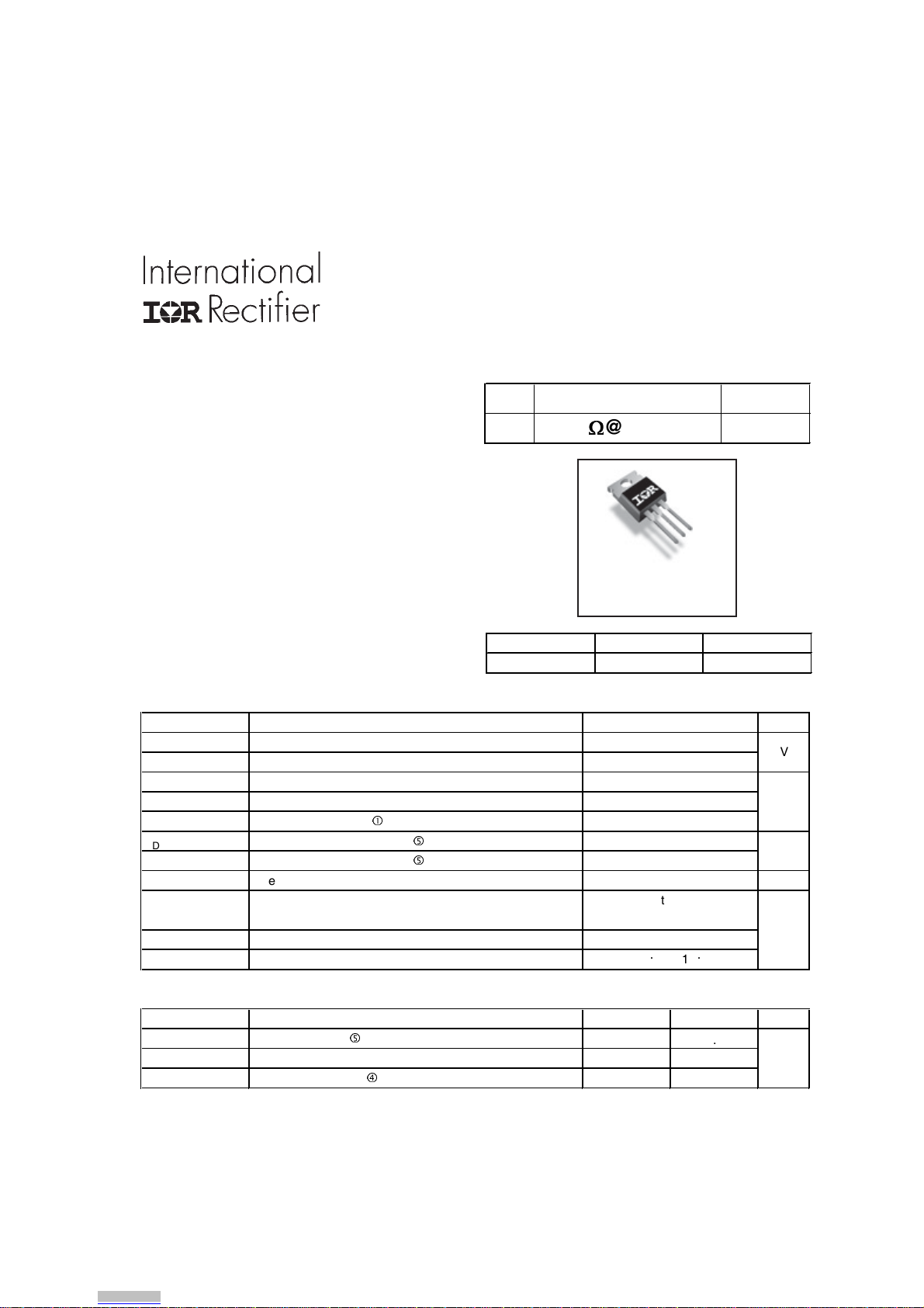
TO-220AB
IRLB8721PbF
S
D
G
D
Applications
Benefits
l Very Low RDS(on) at 4.5V V
GS
l Ultra-Low Gate Impedance
l Fully Characterized Avalanche Voltage
and Current
l Lead-Free
l Optimized for UPS/Inverter Applications
l High Frequency Synchronous Buck
Converters for Computer Processor Power
l High Frequency Isolated DC-DC
Converters with Synchronous Rectification
for Telecom and Industrial Use
V
DSS
R
DS(on)
max
Qg (typ.)
30V
8.7m
:
@VGS = 10V
7.6nC
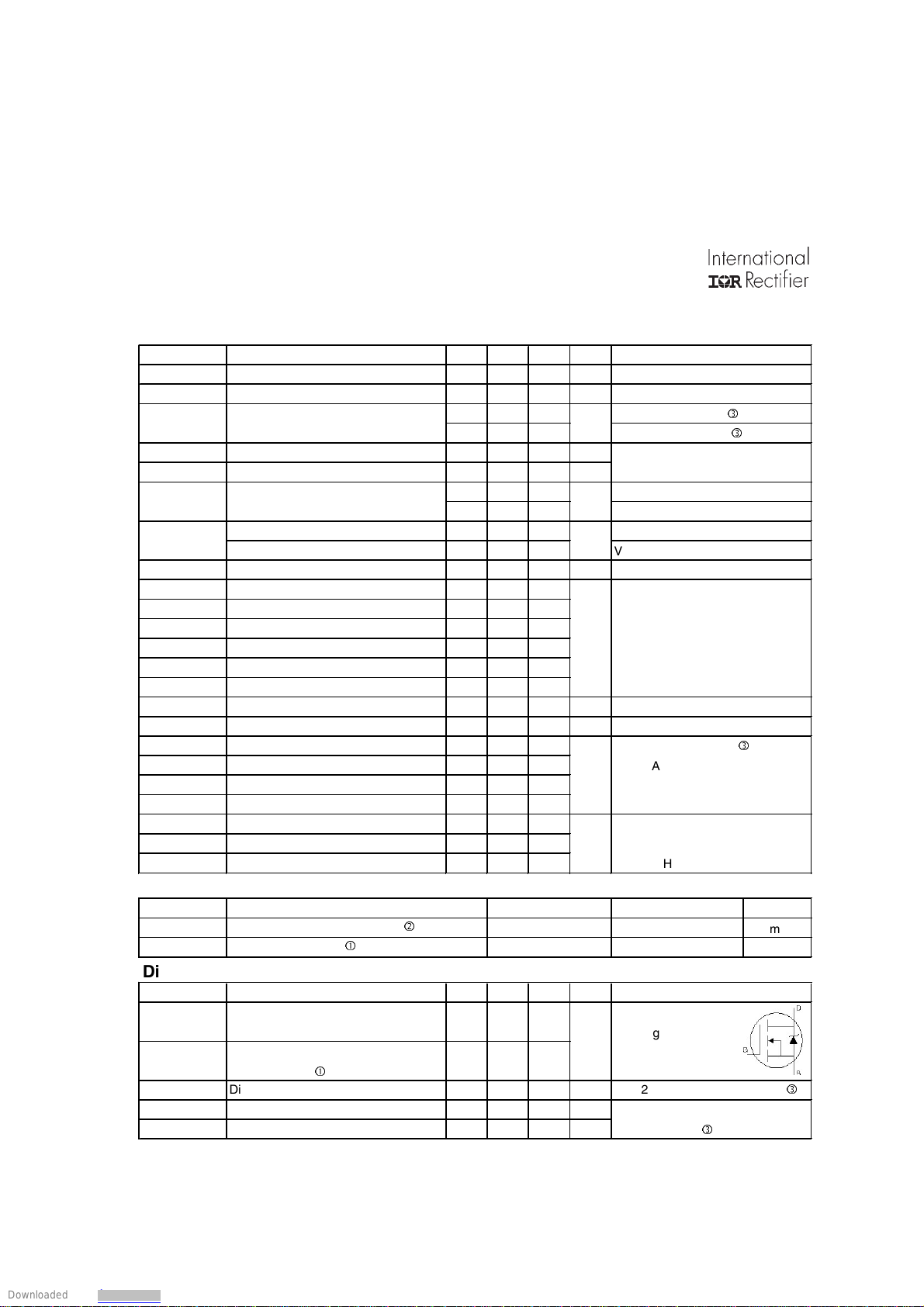
Absolute Maximum Ratings
Parameter Units
V
DS
Drain-to-Source Voltage
V
GS
Gate-to-Source Voltage
I
D
@ TC = 25°C
Continuous Drain Current, V
GS
@ 10V
I
D
@ TC = 100°C
Continuous Drain Current, V
GS
@ 10V
I
DM
Pulsed Drain Current
c
PD @TC = 25°C
Maximum Power Dissipation
g
PD @TC = 100°C
Maximum Power Dissipation
g
Linear Derating Factor
W/°C
T
J
Operating Junction and
T
STG
Storage Temperature Range
Soldering Temperature, for 10 seconds
Mounting torque, 6-32 or M3 screw
Thermal Resistance
Parameter Typ. Max. Units
R
θJC
Junction-to-Case
g
––– 2.3
R
θCS
Case-to-Sink, Flat Greased Surface
0.5 –––
R
θJA
Junction-to-Ambient
f
––– 62
V
°C
°C/W
W
A
0.43
33
10lb
x
in (1.1Nxm)
-55 to + 175
300 (1.6mm from case)
65
Max.
62
250
± 20
30
44
Downloaded from Arrow.com.
IRLB8721PbF
2 www.irf.com
Static @ TJ = 25°C (unless otherwise specified)
Parameter Min. Typ. Max. Units
BV
DSS
Drain-to-Source Breakdown Voltage 30 ––– ––– V
ΔΒV
DSS
/ΔTJ Breakdown Voltage Temp. Coefficient ––– 21 ––– mV/°C
R
DS(on)
Static Drain-to-Source On-Resistance ––– 6.5 8.7
m
Ω
––– 13.1 16
V
GS(th)
Gate Threshold Voltage 1.35 1.80 2.35 V
ΔV
GS(th)
/ΔTJGate Threshold Voltage Coefficient ––– -7.0 ––– mV/°C
I
DSS
Drain-to-Source Leakage Current ––– ––– 1.0 μA
––– ––– 150
I
GSS
Gate-to-Source Forward Leakage ––– ––– 100 nA
Gate-to-Source Reverse Leakage ––– ––– -100
gfs Forward Transconductance 35 ––– ––– S
Q
g
Total Gate Charge ––– 7.6 13
Q
gs1
Pre-Vth Gate-to-Source Charge ––– 1.9 –––
Q
gs2
Post-Vth Gate-to-Source Charge ––– 1.2 ––– nC
Q
gd
Gate-to-Drain Charge ––– 3.4 –––
Q
godr
Gate Charge Overdrive ––– 2.0 ––– See Fig. 16
Q
sw
Switch Charge (Q
gs2
+ Qgd) ––– 4.6 –––
Q
oss
Output Charge ––– 7.9 ––– nC
R
G
Gate Resistance ––– 2.3 3.8
Ω
t
d(on)
Turn-On Delay Time ––– 9.1 –––
t
r
Rise Time ––– 93 –––
t
d(off)
Turn-Off Delay Time ––– 9.0 ––– ns
t
f
Fall Time ––– 17 –––
C
iss
Input Capacitance ––– 1077 –––
C
oss
Output Capacitance ––– 360 ––– pF
C
rss
Reverse Transfer Capacitance ––– 110 –––
Avalanche Characteristics
Parameter Units
E
AS
Single Pulse Avalanche Energy
d
mJ
I
AR
Avalanche Current
c
A
Diode Characteristics
Parameter Min. Typ. Max. Units
I
S
Continuous Source Current ––– ––– 62
(Body Diode) A
I
SM
Pulsed Source Current ––– ––– 250
(Body Diode)
c
V
SD
Diode Forward Voltage ––– ––– 1.0 V
t
rr
Reverse Recovery Time ––– 16 24 ns
Q
rr
Reverse Recovery Charge ––– 14 21 nC
Typ.
–––
–––
I
D
= 25A
V
GS
= 0V
V
DS
= 15V
R
G
= 1.8
Ω
Max.
98
25
T
J
= 25°C, IF = 25A, VDD = 15V
di/dt = 200A/μs
e
TJ = 25°C, IS = 25A, VGS = 0V
e
showing the
integral reverse
p-n junction diode.
MOSFET symbol
V
DS
= 15V, ID = 25A
V
DS
= 15V, VGS = 0V
V
DD
= 15V, VGS = 4.5V
e
ID = 25A
V
DS
= 15V
Conditions
See Fig. 14
V
GS
= 4.5V
Conditions
VGS = 0V, ID = 250μA
Reference to 25°C, I
D
= 1mA
V
GS
= 10V, ID = 31A
e
ƒ = 1.0MHz
V
GS
= 4.5V, ID = 25A
e
VGS = 20V
V
GS
= -20V
V
DS
= VGS, ID = 25μA
V
DS
= 24V, VGS = 0V
V
DS
= 24V, VGS = 0V, TJ = 125°C
Downloaded from Arrow.com.Downloaded from Arrow.com.
IRLB8721PbF
www.irf.com 3
Fig 4. Normalized On-Resistance
vs. Temperature
Fig 2. Typical Output CharacteristicsFig 1. Typical Output Characteristics
Fig 3. Typical Transfer Characteristics
0.1 1 10 100
VDS, Drain-to-Source Voltage (V)
1
10
100
1000
I
D
,
D
r
a
i
n
-
t
o
-
S
o
u
r
c
e
C
u
r
r
e
n
t
(
A
)
≤ 60μs PULSE WIDTH
Tj = 25°C
3.0V
VGS
TOP 10V
9.0V
7.0V
5.5V
4.5V
4.0V
3.5V
BOTTOM 3.0V
0.1 1 10 100
VDS, Drain-to-Source Voltage (V)
1
10
100
1000
I
D
,
D
r
a
i
n
-
t
o
-
S
o
u
r
c
e
C
u
r
r
e
n
t
(
A
)
≤ 60μs PULSE WIDTH
Tj = 175°C
3.0V
VGS
TOP 10V
9.0V
7.0V
5.5V
4.5V
4.0V
3.5V
BOTTOM 3.0V
0.0 2.0 4.0 6.0 8.0
VGS, Gate-to-Source Voltage (V)
0.1
1
10
100
1000
I
D
,
D
r
a
i
n
-
t
o
-
S
o
u
r
c
e
C
u
r
r
e
n
t
(
A
)
V
DS
= 15V
≤ 60μs PULSE WIDTH
TJ = 25°C
TJ = 175°C
-60 -40 -20 0 20 40 60 80 100 120 140 160 180
TJ , Junction Temperature (°C)
0.5
1.0
1.5
2.0
R
D
S
(
o
n
)
,
D
r
a
i
n
-
t
o
-
S
o
u
r
c
e
O
n
R
e
s
i
s
t
a
n
c
e
(
N
o
r
m
a
l
i
z
e
d
)
ID = 25A
V
GS
= 10V
Downloaded from Arrow.com.Downloaded from Arrow.com.Downloaded from Arrow.com.
 Loading...