

INFINEON IRLB4030PBF Datasheet
Applications
)
l DC Motor Drive
l High Efficiency Synchronous Rectification in SMPS
l Uninterruptible Power Supply
l High Speed Power Switching
l Hard Switched and High Frequency Circuits
PD - 97369
IRLB4030PbF
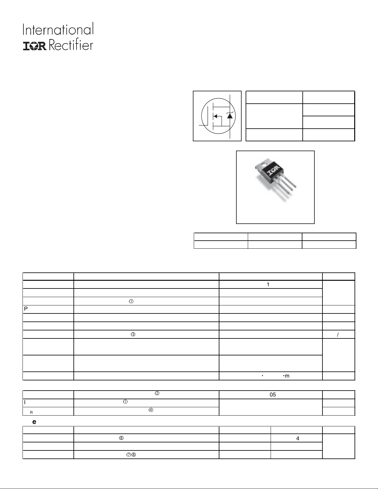
HEXFET® Power MOSFET
D
V
DSS
R
DS(on
G
max.
typ.
100V
3.4m
4.3m
Ω
Ω
Benefits
l Optimized for Logic Level Drive
l Very Low R
l Superior R*Q at 4.5V V
l Improved Gate, Avalanche and Dynamic dV/dt
DS(ON)
at 4.5V V
GS
GS
S
D
I
Ruggedness
l Fully Characterized Capacitance and Avalanche
SOA
l Enhanced body diode dV/dt and dI/dt Capability
l Lead-Free
TO-220AB
GDS
Gate Drain Source
S
D
G
Absolute Maximum Ratings
Symbol Parameter Units
ID @ TC = 25°C
I
@ TC = 100°C Continuous Drain Current, VGS @ 10V
D
I
DM
PD @TC = 25°C
V
GS
dv/dt
T
J
T
STG
Continuous Drain Current, V
Pulsed Drain Current
Maximum Power Dissipation
Linear Derating Factor
Gate-to-Source Voltage
Peak Diode Recovery
Operating Junction and
Storage Temperature Range
Soldering Temperature, for 10 seconds
(1.6mm from case)
Mounting torque, 6-32 or M3 screw
c
e
@ 10V
GS
Max.
180
130
730
370
2.5
± 16
21
-55 to + 175
300
x
in (1.1Nxm)
10lb
Avalanche Characteristics
f
d
305
See Fig. 14, 15, 22a, 22b,
E
AS (Thermally limited)
I
AR
E
AR
Single Pulse Avalanche Energy
Avalanche Current
Repetitive Avalanche Energy
c
Thermal Resistance
Symbol Parameter Typ. Max. Units
R
θ
JC
R
θ
CS
R
θ
JA
Junction-to-Case
Case-to-Sink, Flat, Greased Surface
Junction-to-Ambient
j
ij
–––
0.50 –––
––– 62
0.40
180A
A
W
W/°C
V
V/ns
°C
mJ
A
mJ
°C/W
www.irf.com 1
02/12/09
IRLB4030PbF
/
g
g
h
di/dt = 100A/µs
f
Static @ TJ = 25°C (unless otherwise specified)
Symbol Parameter Min. Typ. Max. Units
V
(BR)DSS
∆V
(BR)DSS
R
DS(on)
V
GS(th)
I
DSS
I
GSS
R
G(int)
Dynamic @ TJ = 25°C (unless otherwise specified)
Symbol Parameter Min. Typ. Max. Units
fs Forward Transconductance 320 ––– ––– S
Q
g
Q
gs
Q
gd
Q
sync
t
d(on)
t
r
t
d(off)
t
f
C
iss
C
oss
C
rss
C
eff. (ER)
oss
C
eff. (TR)
oss
Drain-to-Source Breakdown Voltage 100 ––– ––– V
∆T
Breakdown Voltage Temp. Coefficient ––– 0.10 ––– V/°C
J
Static Drain-to-Source On-Resistance ––– 3.4 4.3
––– 3.6 4.5
Gate Threshold Voltage 1.0 ––– 2.5 V
Drain-to-Source Leakage Current ––– ––– 20
––– ––– 250
Gate-to-Source Forward Leakage ––– ––– 100
Gate-to-Source Reverse Leaka
Internal Gate Resistance
e ––– ––– -100
–––
2.1 –––
Total Gate Charge ––– 87 130
Gate-to-Source Charge ––– 27 –––
Gate-to-Drain ("Miller") Charge ––– 45 –––
Total Gate Charge Sync. (Qg - Qgd)
––– 42 –––
Turn-On Delay Time ––– 74 –––
Rise Time ––– 330 –––
Turn-Off Delay Time ––– 110 –––
Fall Time ––– 170 –––
Input Capacitance ––– 11360 –––
Output Capacitance ––– 670 –––
Reverse Transfer Capacitance ––– 290 –––
Effective Output Capacitance (Energy Related)
Effective Output Capacitance (Time Related)
––– 760 –––
––– 1140 –––
g
Conditions
VGS = 0V, ID = 250µA
Reference to 25°C, I
VGS = 10V, ID = 110A
mΩ
V
= 4.5V, ID = 92A
GS
VDS = VGS, ID = 250µA
V
= 100V, VGS = 0V
DS
µA
V
= 100V, VGS = 0V, TJ = 125°C
DS
= 16V
V
GS
nA
V
= -16V
GS
Ω
Conditions
VDS = 25V, ID = 110A
I
= 110A
D
V
= 50V
DS
nC
ns
pF
= 4.5V
V
GS
= 110A, VDS =0V, VGS = 4.5V
I
D
f
VDD = 65V
I
= 110A
D
R
= 2.7
Ω
G
VGS = 4.5V
f
VGS = 0V
V
= 50V
DS
ƒ = 1.0MHz
V
= 0V, VDS = 0V to 80V
GS
VGS = 0V, VDS = 0V to 80V
= 5mA
D
f
f
c
h
g
Diode Characteristics
Symbol Parameter Min. Typ. Max. Units
I
S
I
SM
V
SD
t
rr
Q
rr
I
RRM
t
on
Notes:
Repetitive rating; pulse width limited by max. junction
temperature.
Limited by T
RG = 25Ω, I
above this value .
I
≤ 110A, di/dt ≤ 1330A/µs, V
SD
Pulse width ≤ 400µs; duty cycle ≤ 2%.
Continuous Source Current
(Body Diode)
Pulsed Source Current
(Body Diode)
c
––– –––
––– –––
180
730
Diode Forward Voltage ––– ––– 1.3 V
Reverse Recovery Time ––– 50 –––
––– 60 –––
Reverse Recovery Charge ––– 88 –––
––– 130 –––
Reverse Recovery Current ––– 3.3 ––– A
Forward Turn-On Time Intrinsic turn-on time is negligible (turn-on is dominated by LS+LD)
C
eff. (TR) is a fixed capacitance that gives the same charging time
oss
, starting TJ = 25°C, L = 0.05mH
Jmax
= 110A, VGS =10V. Part not recommended for use
AS
as C
C
C
while V
oss
eff. (ER) is a fixed capacitance that gives the same energy as
oss
while V
oss
is rising from 0 to 80% V
DS
is rising from 0 to 80% V
DS
When mounted on 1" square PCB (FR-4 or G-10 Material). For
DD
≤ V
(BR)DSS
, TJ ≤ 175°C.
recommended footprint and soldering techniquea refer to applocation
note # AN- 994 echniques refer to application note #AN-994.
R
is measured at TJ approximately 90°C.
θ
Conditions
MOSFET symbol
showing the
A
integral reverse
p-n junction diode.
TJ = 25°C, IS = 110A, VGS = 0V
= 25°C VR = 85V,
T
J
ns
T
= 125°C IF = 110A
J
= 25°C
T
J
nC
= 125°C
T
J
= 25°C
T
J
.
DSS
.
DSS
D
G
S
f
2 www.irf.com
IRLB4030PbF
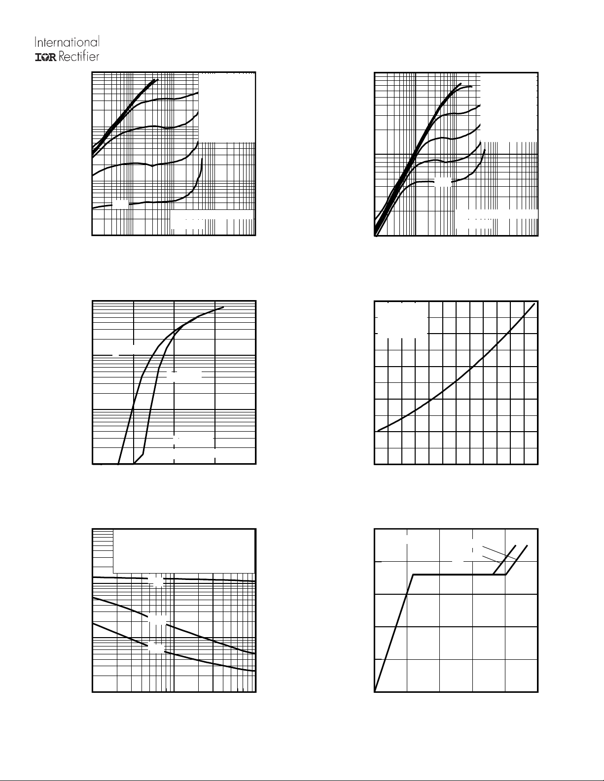
1000
TOP 15V
)
A
(
t
n
e
r
100
r
u
C
e
c
r
u
o
S
o
t
-
10
n
i
a
r
D
,
D
I
2.5V
≤
BOTTOM 2.5V
60µs PULSE WIDTH
Tj = 25°C
1
0.1 1 10 100 1000
VDS, Drain-to-Source Voltage (V)
Fig 1. Typical Output Characteristics
1000
)
A
(
t
n
e
r
100
r
u
C
e
c
r
u
o
S
o
t
-
10
n
i
a
r
D
,
D
I
TJ = 175°C
TJ = 25°C
V
= 50V
DS
60µs PULSE WIDTH
≤
1.0
1 2 3 4 5
VGS, Gate-to-Source Voltage (V)
Fig 3. Typical Transfer Characteristics
VGS
10V
8.0V
4.5V
3.5V
3.0V
2.7V
1000
VGS
10V
8.0V
4.5V
3.5V
3.0V
2.7V
)
A
(
t
n
e
r
r
u
C
e
c
r
u
o
S
o
t
n
i
a
r
D
,
I
100
D
2.5V
60µs PULSE WIDTH
≤
TOP 15V
BOTTOM 2.5V
Tj = 175°C
10
0.1 1 10 100 1000
VDS, Drain-to-Source Voltage (V)
Fig 2. Typical Output Characteristics
2.5
e
c
n
a
t
s
i
s
e
R
n
O
)
e
d
c
r
e
u
z
i
l
o
a
S
-
m
o
r
t
-
o
n
N
i
(
a
r
D
,
)
n
o
(
S
D
R
2.0
1.5
1.0
0.5
ID = 110A
V
= 10V
GS
0.0
-60 -40 -20 0 20 40 60 80 100120140160180
TJ , Junction Temperature (°C)
Fig 4. Normalized On-Resistance vs. Temperature
100000
)
F
10000
p
(
e
c
n
a
t
i
c
a
p
a
C
1000
,
C
100
V
= 0V, f = 1 MHZ
GS
C
= C
C
C
iss
rss
oss
= C
= C
gs
gd
ds
C
iss
C
oss
C
rss
+ Cgd, C
+ C
SHORTED
ds
gd
1 10 100
VDS, Drain-to-Source Voltage (V)
5.0
ID= 110A
)
V
4.0
(
e
g
a
t
l
o
V
3.0
e
c
r
u
o
S
o
2.0
t
e
t
a
G
,
S
1.0
G
V
VDS= 80V
VDS= 50V
0.0
0 20406080100
QG, Total Gate Charge (nC)
Fig 6. Typical Gate Charge vs. Gate-to-Source VoltageFig 5. Typical Capacitance vs. Drain-to-Source Voltage
www.irf.com 3
 Loading...