


Applications
A
)
l Primary Side Switch in Bridge Topology
in Universal Input (36-75Vin) Isolated
DC-DC Converters
l Primary Side Switch in Push-Pull
Topology for 18-36Vin Isolated DC-DC
Converters
l Secondary Side Synchronous
Rectification Switch for 15Vout
l Suitable for 48V Non-Isolated
Synchronous Buck DC-DC Applications
Benefits
l Low Gate to Drain Charge to Reduce
Switching Losses
l Fully Characterized Capacitance Including
Effective C
to Simplify Design, (See
OSS
App. Note AN1001)
l Fully Characterized Avalanche Voltage
and Current
Absolute Maximum Ratings
Parameter Units
V
DS
V
GS
@ TA = 25°C
I
D
I
@ TA = 70°C
D
I
DM
PD @TA = 25°C
dv/dt
T
J
T
STG
Drain-to-Source Voltage V
Gate-to-Source Voltage
Continuous Drain Current, V
Continuous Drain Current, V
Pulsed Drain Current
Maximum Power Dissipation
Linear Derating Factor W/°C
Peak Diode Recovery dv/dt
Operating Junction and °C
Storage Temperature Range
c
@ 10V A
GS
@ 10V
GS
h
V
DSS
100V
S
S
S
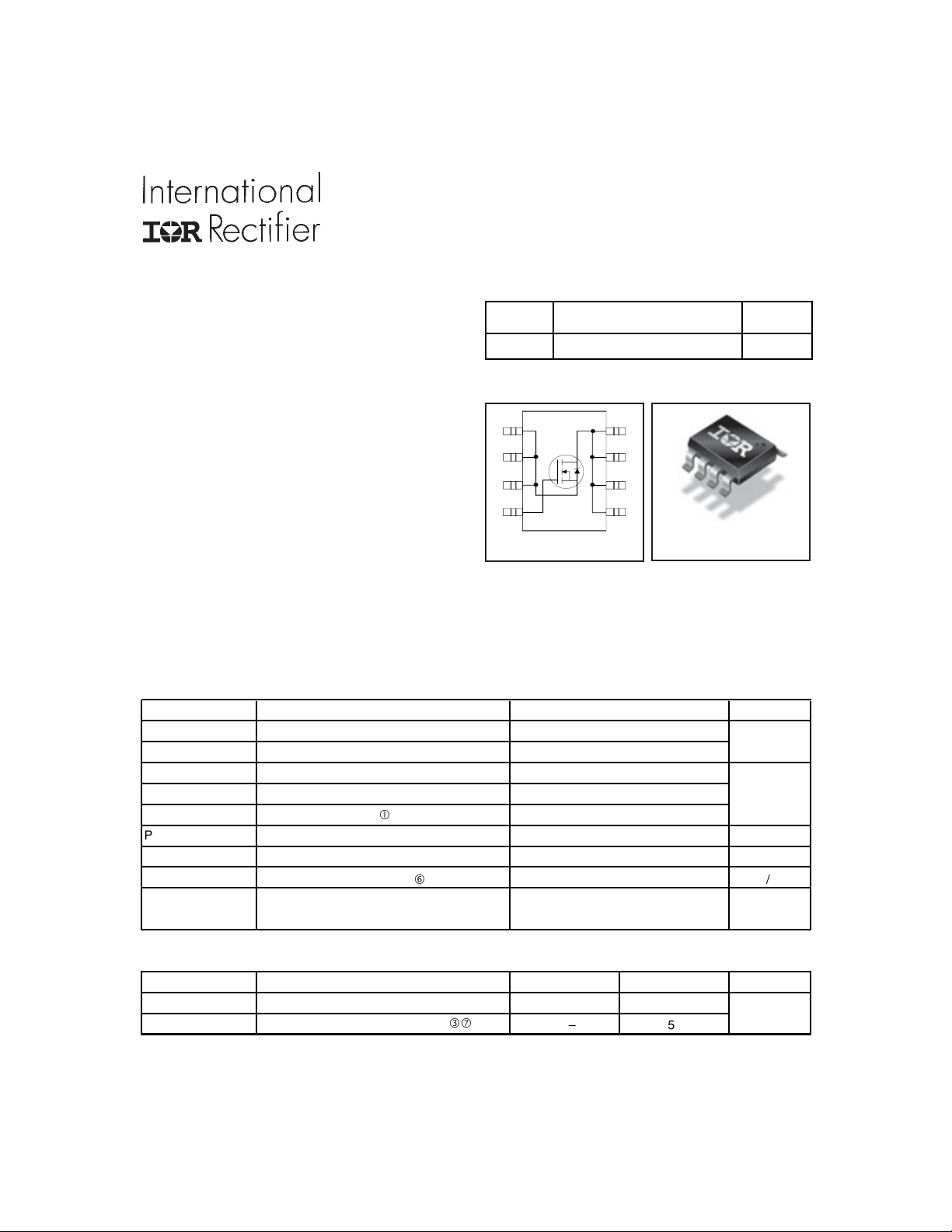
IRF7853PbF
HEXFET® Power MOSFET
R
DS(on
18m:@VGS = 10V
1
2
3
4
Top View
A
8
D
7
D
6
D
5
DG
Max.
100
± 20
8.3
6.6
66
2.5
0.02
5.1
-55 to + 150
PD - 97069
max I
8.3A
SO-8
V/ns
D
W
Thermal Resistance
Parameter Typ. Max. Units
R
θJL
R
θJA
Notes through are on page 8
www.irf.com 1
Junction-to-Drain Lead ––– 20 °C/W
Junction-to-Ambient (PCB Mount)
ei
––– 50
1/5/06
IRF7853PbF
Static @ T
= 25°C (unl
ified)
D
@ T
= 25°C (unl
ified)
J
V
(BR)DSS
∆V
R
DS(on)
V
GS(th)
I
DSS
I
GSS
(BR)DSS
Drain-to-Source Breakdown Voltage 100 ––– ––– V
/∆TJ Breakdown Voltage Temp. Coefficient ––– 0.11 ––– V/°C
Static Drain-to-Source On-Resistance ––– 14.4 18
Gate Threshold Voltage 3.0 ––– 4.9 V
Drain-to-Source Leakage Current ––– ––– 20 µA
Gate-to-Source Forward Leakage ––– ––– 100 nA
Gate-to-Source Reverse Leakage ––– ––– -100
ynamic
J
gfs Forward Transconductance 11 ––– ––– S
Q
g
Q
gs
Q
gd
R
G
t
d(on)
t
r
t
d(off)
t
f
C
iss
C
oss
C
rss
C
oss
C
oss
eff. Effective Output Capacitance ––– 320 –––
C
oss
Total Gate Charge ––– 28 39
Gate-to-Source Charge ––– 7.8 ––– nC
Gate-to-Drain ("Miller") Charge ––– 10 –––
Gate Resistance ––– 1.4 –––
Turn-On Delay Time ––– 13 –––
Rise Time ––– 6.6 –––
Turn-Off Delay Time ––– 26 ––– ns
Fall Time ––– 6.0 –––
Input Capacitance ––– 1640 –––
Output Capacitance ––– 310 –––
Reverse Transfer Capacitance ––– 71 ––– pF
Output Capacitance ––– 1600 –––
Output Capacitance ––– 180 –––
ess otherwise spec
Parameter Min. Typ. Max. Units
mΩ
––– ––– 250
ess otherwise spec
Parameter Min. Typ. Max. Units
Ω
Conditions
VGS = 0V, ID = 250µA
Reference to 25°C, I
V
= 10V, ID = 8.3A
GS
= 1mA
D
f
VDS = VGS, ID = 100µA
= 100V, VGS = 0V
V
DS
= 100V, VGS = 0V, TJ = 125°C
V
DS
VGS = 20V
= -20V
V
GS
Conditions
VDS = 25V, ID = 5.0A
= 5.0A
I
D
= 50V
V
DS
VGS = 10V
VDD = 50V
= 5.0A
I
D
R
G
VGS = 10V
VGS = 0V
V
DS
ƒ = 1.0MHz
V
GS
V
GS
V
GS
f
= 6.2Ω
f
= 25V
= 0V, VDS = 1.0V, ƒ = 1.0MHz
= 0V, VDS = 80V, ƒ = 1.0MHz
= 0V, VDS = 0V to 80V
g
Avalanche Characteristics
Parameter Units
E
AS
I
AR
Single Pulse Avalanche Energy
Avalanche Current
c
d
Typ.
–––
–––
Max.
610
5.0
Diode Characteristics
Parameter Min. Typ. Max. Units
I
S
Continuous Source Current ––– ––– 2.3
(Body Diode) A
I
SM
V
SD
t
rr
Q
rr
t
on
Pulsed Source Current ––– ––– 66
(Body Diode)
c
Diode Forward Voltage ––– ––– 1.3 V
Reverse Recovery Time ––– 45 68 ns
Reverse Recovery Charge ––– 84 130 nC
Forward Turn-On Time Intrinsic turn-on time is negligible (turn-on is dominated by LS+LD)
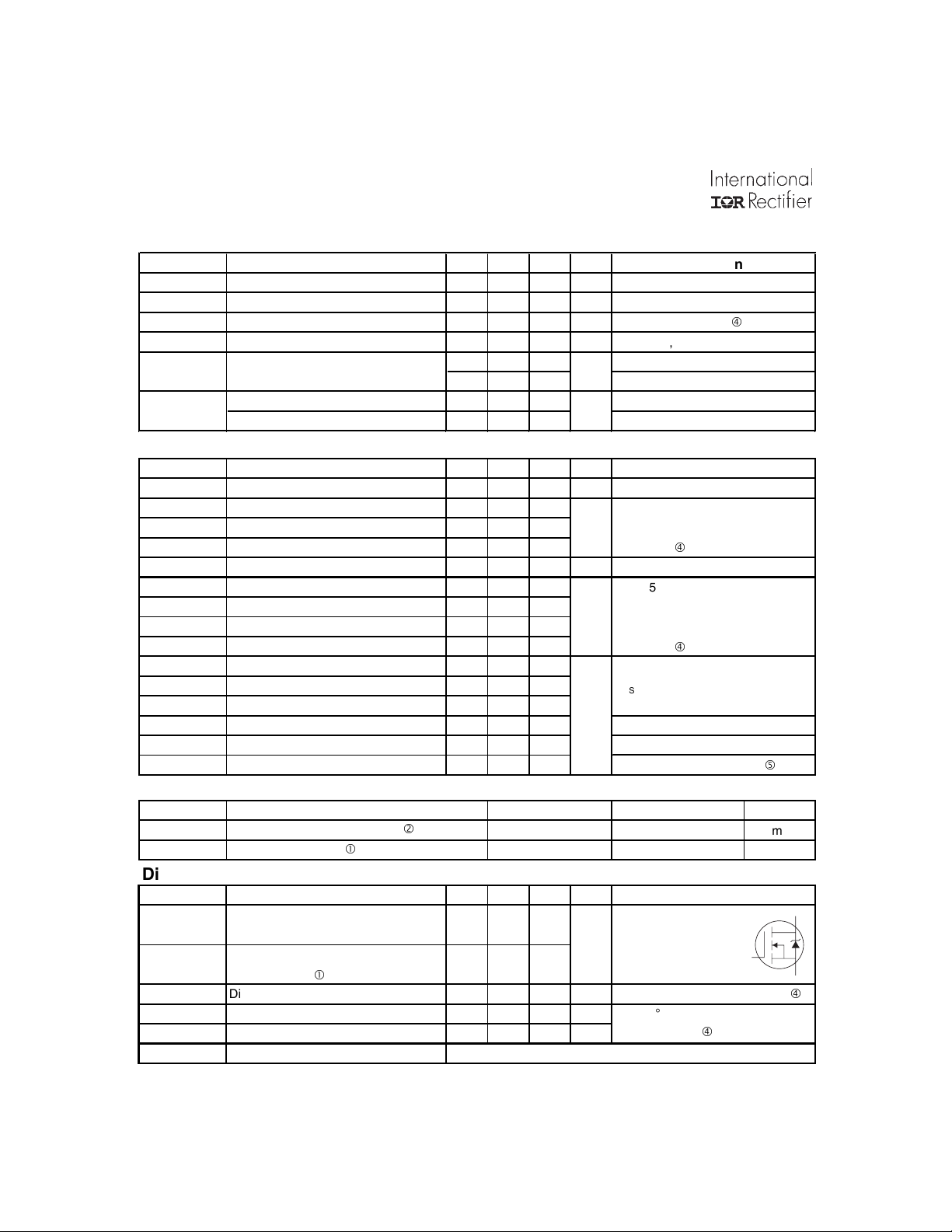
MOSFET symbol
showing the
integral reverse
p-n junction diode.
T
= 25°C, IS = 5.0A, VGS = 0V
J
TJ = 25°C, IF = 5.0A, VDD = 25V
di/dt = 100A/µs
Conditions
G
f
2 www.irf.com
mJ
A
D
S
f
IRF7853PbF
100
)
A
(
t
n
e
r
r
u
C
e
c
r
u
o
S
o
t
n
i
a
r
D
,
D
I
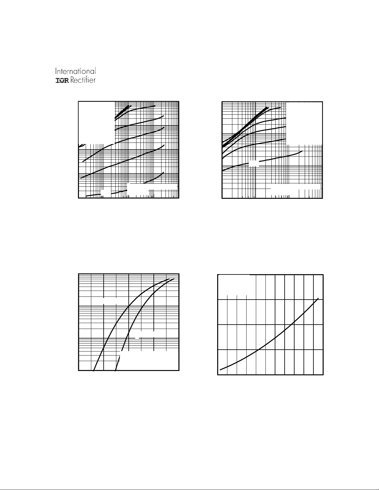
TOP 15V
10
BOTTOM 4.5V
1
0.1
0.01
0.01 0.1 1 10 100
VGS
10V
8.0V
7.0V
6.0V
5.5V
5.0V
4.5V
≤
60µs PULSE WIDTH
Tj = 25°C
VDS, Drain-to-Source Voltage (V)
100.0
)
Α
(
t
n
e
r
r
10.0
u
C
e
c
r
u
o
S
o
t
n
1.0
i
a
r
D
,
D
I
0.1
3.0 4.0 5.0 6.0 7.0
TJ = 150°C
V
≤
TJ = 25°C
= 25V
DS
60µs PULSE WIDTH
VGS, Gate-to-Source Voltage (V)
100
)
A
(
t
n
e
r
r
10
u
C
e
c
r
u
o
S
o
t
n
1
i
a
r
D
,
D
I
4.5V
TOP 15V
BOTTOM 4.5V
≤
60µs PULSE WIDTH
VGS
10V
8.0V
7.0V
6.0V
5.5V
5.0V
Tj = 150°C
0.1
0.1 1 10 100
VDS, Drain-to-Source Voltage (V)
Fig 2. Typical Output CharacteristicsFig 1. Typical Output Characteristics
2.5
e
c
n
a
t
s
i
s
e
R
n
O
e
c
r
u
o
S
o
t
n
i
a
r
D
,
)
n
o
(
S
D
R
ID = 8.3A
V
= 10V
GS
2.0
)
d
e
z
i
l
a
1.5
m
r
o
N
(
1.0
0.5
-60 -40 -20 0 20 40 60 80 100 120 140 160
TJ , Junction Temperature (°C)
Fig 3. Typical Transfer Characteristics
Fig 4. Normalized On-Resistance
vs. Temperature
www.irf.com 3