

g
PD - 95466
AUTOMOTIVE MOSFET
Features
● Advanced Process Technology
● Ultra Low On-Resistance
● Dynamic dv/dt Rating
● 175°C Operating Temperature
● Fast Switching
● Repetitive Avalanche Allowed up to Tjmax
● Lead-Free
Description
Specifically designed for Automotive applications,
this HEXFET® Power MOSFET utilizes the latest
processing techniques to achieve extremely low
on-resistance per silicon area. Additional features of this design are a 175°C junction operating
temperature, fast switching speed and improved
repetitive avalanche rating . These features combine to make this design an extremely efficient
and reliable device for use in Automotive applications and a wide variety of other applications.
G
TO-220AB
IRF3710Z
IRF3710ZPbF
IRF3710ZSPbF
IRF3710ZLPbF
HEXFET® Power MOSFET
D
S
IRF3710ZS
D2Pak
V
R
DS(on)
DSS
= 100V
= 18mΩ
ID = 59A
TO-262
IRF3710ZL
Absolute Maximum Ratings
ID @ TC = 25°C
I
@ TC = 100°C
D
I
DM
PD @TC = 25°C
V
GS
E
AS
E
(tested)
AS
I
AR
E
AR
T
J
T
STG
Continuous Drain Current, V
Continuous Drain Current, V
Pulsed Drain Current
Maximum Power Dissipation W
Linear Derating Factor W/°C
Gate-to-Source Voltage V
Single Pulse Avalanche Energy (Thermally Limited)
le Pulse Avalanche Energy Tested Value
Sin
Avalanche Current
Repetitive Avalanche Energy
Operating Junction and °C
Storage Temperature Range
Soldering Temperature, for 10 seconds
Mounting torque, 6-32 or M3 screw
Thermal Resistance
R
JC
θ
R
CS
θ
R
JA
θ
R
JA
θ
Junct ion-to-Case ––– 0.92 °C/W
Case-to-Sink, Flat, Greased Surface
Junct ion-to-Ambient ––– 62
Junct ion-to-Ambient (PCB Mount, steady state)
Parameter Units
@ 10V (Silicon Limited)
GS
@ 10V (See Fig. 9)
GS
c
d
i
c
h
See Fig.12a,12b,15,16
300 (1.6mm from case )
Max.
59
42
240
160
1.1
± 20
170
200
-55 to + 175
10 lbf•in (1.1N•m)
Parameter Typ. Max. Units
0.50 –––
j
––– 40
A
mJ
A
mJ
HEXFET® is a registered trademark of International Rectifier.
www.irf.com 1
6/30/04
IRF3710Z/S/LPbF
/
g
g
Static @ TJ = 25°C (unless otherwise specified)
V
(BR)DSS
∆ΒV
R
DS(on)
V
GS(th)
DSS
Drain-to-Source Breakdown Voltage 100 ––– ––– V
∆T
Breakdown Voltage Temp. Coefficient ––– 0.10 ––– V/°C
J
Static Drain-to-Source On-Resistance ––– 14 18
Gate Threshold Voltage 2.0 ––– 4.0 V
fs Forward Transconductance 35 ––– ––– S
I
I
DSS
GSS
Drain-to-Source Leakage Current ––– ––– 20 µA
Gate-to-Source Forward Leakage ––– ––– 200 nA
Gate-to-Source Reverse Leaka
Q
Q
Q
t
t
t
t
L
L
C
C
C
C
C
C
g
gs
gd
d(on)
r
d(off)
f
D
S
iss
oss
rss
oss
oss
oss
eff.
Total Gate Charge ––– 82 120 nC
Gate-to-Source Charge ––– 19 28
Gate-to-Drain ("Miller") Charge ––– 27 40
Turn-On Delay Time ––– 17 ––– ns
Rise Time ––– 77 –––
Turn-Off Delay Time ––– 41 –––
Fall Time ––– 56 –––
Internal Drain Inductance ––– 4.5 ––– nH Between lead,
Internal Source Inductance ––– 7.5 ––– from package
Input Capacitance ––– 2900 ––– pF
Output Capacitance ––– 290 –––
Reverse Transfer Capacitance ––– 150 –––
Output Capacitance ––– 1130 –––
Output Capacitance ––– 170 –––
Effective Output Capacitance ––– 280 –––
Parameter Min. Typ. Max. Units
––– ––– 250
e ––– ––– -200
Conditions
VGS = 0V, ID = 250µA
Reference to 25°C, I
V
= 10V, ID = 35A
Ω
m
GS
VDS = VGS, ID = 250µA
V
= 50V, ID = 35A
DS
V
= 100V, VGS = 0V
DS
V
= 100V, VGS = 0V, TJ = 125°C
DS
V
= 20V
GS
V
= -20V
GS
I
= 35A
D
= 80V
V
DS
V
= 10V
GS
V
DD
I
= 35A
D
R
G
V
GS
6mm (0.25in.)
and center of die contact
V
GS
V
DS
ƒ = 1.0MHz, See Fig. 5
V
GS
V
GS
VGS = 0V, VDS = 0V to 80V
f
= 50V
= 6.8Ω
= 10V
f
= 0V
= 25V
= 0V, VDS = 1.0V, ƒ = 1.0MHz
= 0V, VDS = 80V, ƒ = 1.0MHz
= 1mA
D
f
D
G
S
Diode Characteristics
I
S
I
SM
V
SD
t
rr
Q
rr
t
on
Notes:
Continuous Source Current ––– ––– 59
(Body Diode) A
Pulsed Source Current ––– ––– 240
(Body Diode)
c
Diode Forward Voltage
Reverse Recovery Time
Reverse Recovery Charge ––– 100 160 nC
Forward Turn-On Time Intrinsic turn-on time is negligible (turn-on is dominated by LS+LD)
Repetitive rating; pulse width limited by
Parameter Min. Typ. Max. Units
max. junction temperature. (See fig. 11).
Limited by T
RG = 25Ω, I
, starting TJ = 25°C, L = 0.27mH,
Jmax
= 35A, VGS =10V. Part not
AS
recommended for use above this value.
I
≤ 35A, di/dt ≤ 380A/µs, V
SD
DD
≤ V
(BR)DSS
TJ ≤ 175°C.
Pulse width ≤ 1.0ms; duty cycle ≤ 2%.
MOSFET symbol
showing the
integral reverse
p-n junction diode.
––– ––– 1.3 V
–––5075ns
C
eff. is a fixed capacitance that gives the same charging time
oss
as C
while V
oss
Limited by T
is rising from 0 to 80% V
DS
, see Fig.12a, 12b, 15, 16 for typical repetitive
Jmax
TJ = 25°C, IS = 35A, VGS = 0V
T
= 25°C, IF = 35A, VDD = 25V
J
di/dt = 100A/µs
avalanche performance.
This value determined from sample failure population. 100%
,
tested to this value in production.
This is applied to D
2
Pak, when mounted on 1" square PCB
( FR-4 or G-10 Material ). For recommended footprint and
soldering techniques refer to application note #AN-994.
Conditions
f
.
DSS
G
2 www.irf.com
D
S
f

IRF3710Z/S/LPbF
)
A
(
t
n
e
r
r
u
C
e
c
r
u
o
S
o
t
n
i
a
r
D
,
I
D
1000
100
10
1
0.1
TOP 15V
BOTTOM 4.5V
VGS
10V
8.0V
7.0V
6.0V
5.5V
5.0V
4.5V
20µs PULSE WIDTH
Tj = 25°C
0.01
0.1 1 10 100
VDS, Drain-to-Source Voltage (V)
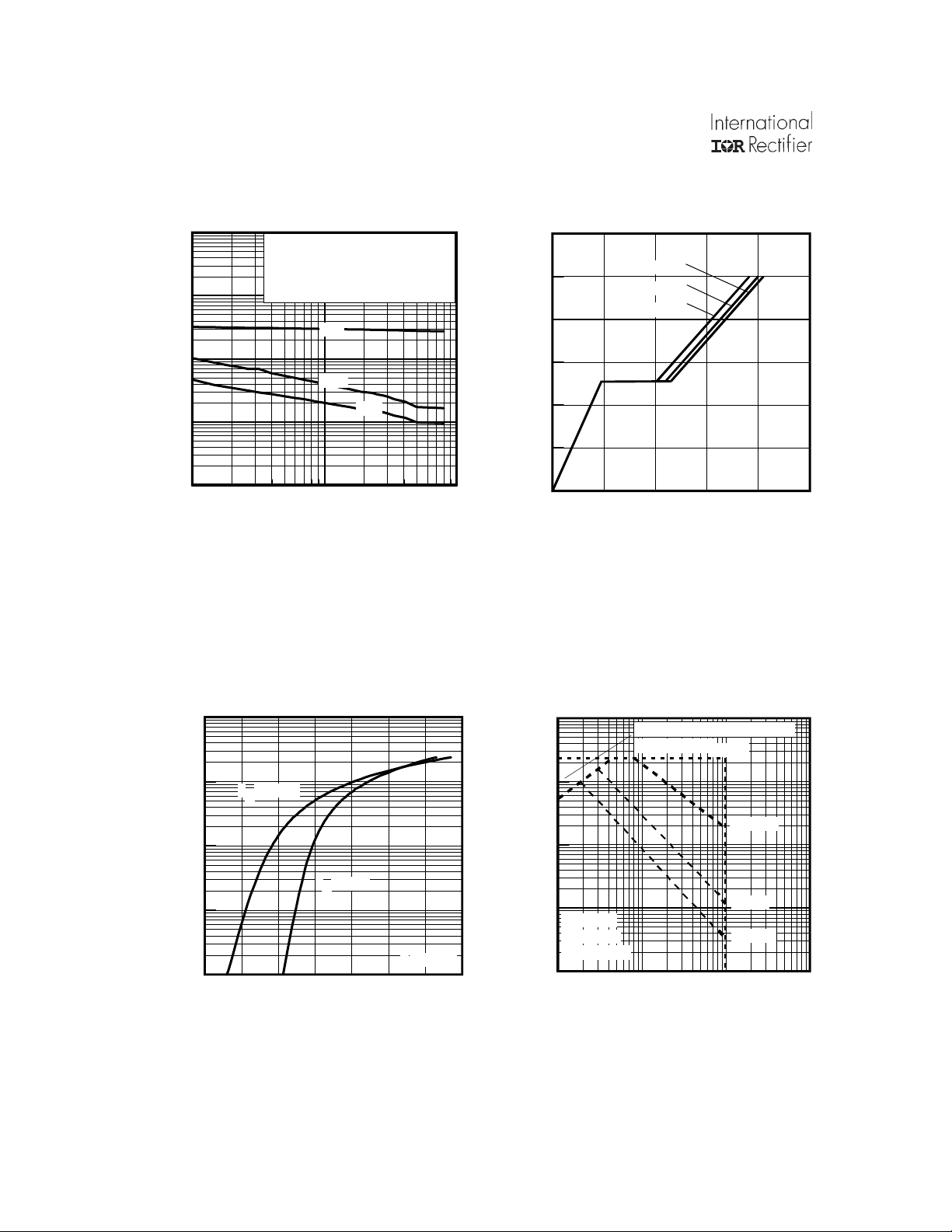
Fig 1. Typical Output Characteristics
)
A
(
t
n
e
r
r
u
C
e
c
r
u
o
S
o
t
n
i
a
r
D
,
I
1000
TOP 15V
100
BOTTOM 4.5V
10
D
VGS
10V
8.0V
7.0V
6.0V
5.5V
5.0V
4.5V
20µs PULSE WIDTH
Tj = 175°C
1
0.1 1 10 100
VDS, Drain-to-Source Voltage (V)
Fig 2. Typical Output Characteristics
1000
)
Α
(
t
100
n
e
r
r
u
C
e
c
r
10
u
o
S
o
t
n
i
a
r
1
D
,
D
I
TJ = 25°C
V
0
2 4 6 8 10
20µs PULSE WIDTH
DS
TJ = 175°C
= 25V
VGS, Gate-to-Source Voltage (V)
Fig 3. Typical Transfer Characteristics
120
)
S
(
100
e
c
n
a
t
c
80
u
d
n
o
c
s
n
60
a
r
T
d
r
a
40
w
r
o
F
,
S
20
F
G
0
0 10 20 30 40 50 60 70
VDS = 15V
20µs PULSE WIDTH
TJ = 25°C
TJ = 175°C
ID, Drain-to-Source Current (A)
Fig 4. Typical Forward Transconductance
vs. Drain Current
www.irf.com 3
IRF3710Z/S/LPbF
100000
10000
)
F
p
(
e
c
n
a
t
i
1000
c
a
p
a
C
,
C
100
10
1 10 100
V
= 0V, f = 1 MHZ
GS
C
= C
iss
rss
oss
= C
= C
gs
gd
ds
C
C
+ Cgd, C
+ C
Ciss
Coss
gd
Crss
VDS, Drain-to-Source Voltage (V)
Fig 5. Typical Capacitance vs.
Drain-to-Source Voltage
SHORTED
ds
12.0
ID= 35A
)
10.0
V
(
e
g
a
t
l
8.0
o
V
e
c
r
u
6.0
o
S
o
t
e
t
4.0
a
G
,
S
G
2.0
V
VDS= 80V
VDS= 50V
VDS= 20V
0.0
0 20406080100
Q
Total Gate Charge (nC)
G
Fig 6. Typical Gate Charge vs.
Gate-to-Source Voltage
1000.00
1000
OPERATION IN THIS AREA
LIMITED BY RDS(on)
)
A
(
100.00
t
n
e
r
r
u
C
n
i
a
r
D
e
s
r
e
v
e
R
,
D
S
I
10.00
1.00
TJ = 175°C
TJ = 25°C
0.10
0.2 0.4 0.6 0.8 1.0 1.2 1.4 1.6
VSD, Source-to-Drain Voltage (V)
Fig 7. Typical Source-Drain Diode
V
= 0V
GS
)
A
(
t
100
n
e
r
r
u
C
e
c
r
u
o
S
o
t
n
i
a
r
D
,
D
I
10
1
Tc = 25°C
Tj = 175°C
100µsec
1msec
10msec
Single Pulse
0.1
1 10 100 1000
V
, Drain-toSource Voltage (V)
DS
Fig 8. Maximum Safe Operating Area
Forward Voltage
4 www.irf.com
 Loading...