

INFINEON IM818-MCC Datasheet

Datasheet Please read the Important Notice and Warnings at the end of this document V 2.1
www.infineon.com page 1 of 21 2018-08-20
IM818-MCC Datasheet
CIPOS™ Maxi IM818
IM818-MCC
Description
The CIPOS™ Maxi IM818 product group offers the chance for integrating various power and control
components to increase reliability, optimize PCB size and system costs. It is designed to control three phase AC
motors and permanent magnet motors in variable speed drives applications such as low power motor drives (GPI,
Servo drives), pumps, fan drives and active filter for HVAC(Heating, Ventilation, and Air Conditioning). The
product concept is specially adapted to power applications, which need good thermal performance and
electrical isolation as well as EMI save control and overload protection.
Three phase inverter with 1200V TRENCHSTOP™ IGBTs and Emitter Controlled diodes are combined with an
optimized 6-channel SOI gate driver for excellent electrical performance.
Features
Fully isolated Dual In-Line molded module
1200V TRENCHSTOP™ IGBT4
Rugged 1200V SOI gate driver technology with stability
against transient and negative voltage
Allowable negative VS potential up to -11 V
for signal transmission at VBS = 15 V
Integrated bootstrap functionality
Over current shutdown
Built-in NTC thermistor for temperature monitor
Under-voltage lockout at all channels
Low side emitter pins accessible
for all phase current monitoring (open emitter)
Cross-conduction prevention
All of 6 switches turn off during protection
Programmable fault clear timing and enable input
Lead-free terminal plating; RoHS compliant
Potential applications
Fan drives and active filter for HVAC, pumps, and low power motor drives (GPI, Servo Drives)
Product validation
Qualified for industrial applications according to the relevant tests of JEDEC47/20/22.
Table 1 Part Ordering Table
Product Name
Package Type
Standard Pack
Orderable Part Number
Form
MOQ
IM818-MCC
DIP 36x23D
14 pcs / tube
280
IM818MCCXKMA1

Datasheet 2 of 21 V 2.1
2018-08-20
CIPOS™ Maxi IM818
IM818-MCC
Table of Contents
Table of Contents
1 Internal Electrical Schematic ................................................................................................... 3
2 Pin Configuration ................................................................................................................... 4
2.1 Pin Assignment ........................................................................................................................................ 4
2.2 Pin Description ........................................................................................................................................ 5
3 Absolute Maximum Ratings ..................................................................................................... 7
3.1 Module Section ........................................................................................................................................ 7
3.2 Inverter Section ....................................................................................................................................... 7
3.3 Control Section ........................................................................................................................................ 7
4 Thermal Characteirstics .......................................................................................................... 8
5 Recommended Operation Conditions ....................................................................................... 9
6 Static Parameters ................................................................................................................. 10
6.1 Inverter Section ..................................................................................................................................... 10
6.2 Control Section ...................................................................................................................................... 10
7 Dynamic Parameters ............................................................................................................. 11
7.1 Inverter Section ..................................................................................................................................... 11
7.2 Control Section ...................................................................................................................................... 11
8 Thermistor Characteristics ..................................................................................................... 12
9 Mechanical Characteristics and Ratings ................................................................................... 13
10 Qualification Information....................................................................................................... 14
11 Diagrams and Tables ............................................................................................................. 15
11.1 TC Measurement Point ........................................................................................................................... 15
11.2 Backside Curvature Measurement Point .............................................................................................. 15
11.3 Switching Time Definition ..................................................................................................................... 16
12 Application Guide .................................................................................................................. 17
12.1 Typical Application Schematic ............................................................................................................. 17
12.2 Performance Charts .............................................................................................................................. 18
13 Package Outline .................................................................................................................... 19
Revision history............................................................................................................................. 20

Datasheet 3 of 21 V 2.1
2018-08-20
CIPOS™ Maxi IM818
IM818-MCC
Internal Electrical Schematic
1 Internal Electrical Schematic
VSS
VDD
LIN3
LIN2
LIN1
RFE
ITRIP
LO3
LO2
LO1
HO1
HO2
HO3
VB1
VS1
VB2
VS2
VB3
VS3
HIN3
HIN2
HIN1
NW (18)
NV (19)
W (21)
V (22)
U (23)
P (24)
(2) VB(U)
(15) ITRIP
(14) RFE
(10) LIN(U)
(11) LIN(V)
(12) LIN(W)
(16) VSS
(13) VDD
(4) VB(V)
(6) VB(W)
(7) HIN(U)
(8) HIN(V)
(9) HIN(W)
(1) VS(U)
(3) VS(V)
(5) VS(W)
NU (20)
Thermistor
RBS1
RBS2
RBS3
(17) VTH
Figure 1 Internal electrical schematic
Datasheet 4 of 21 V 2.1
2018-08-20
CIPOS™ Maxi IM818
IM818-MCC
Pin Configuration
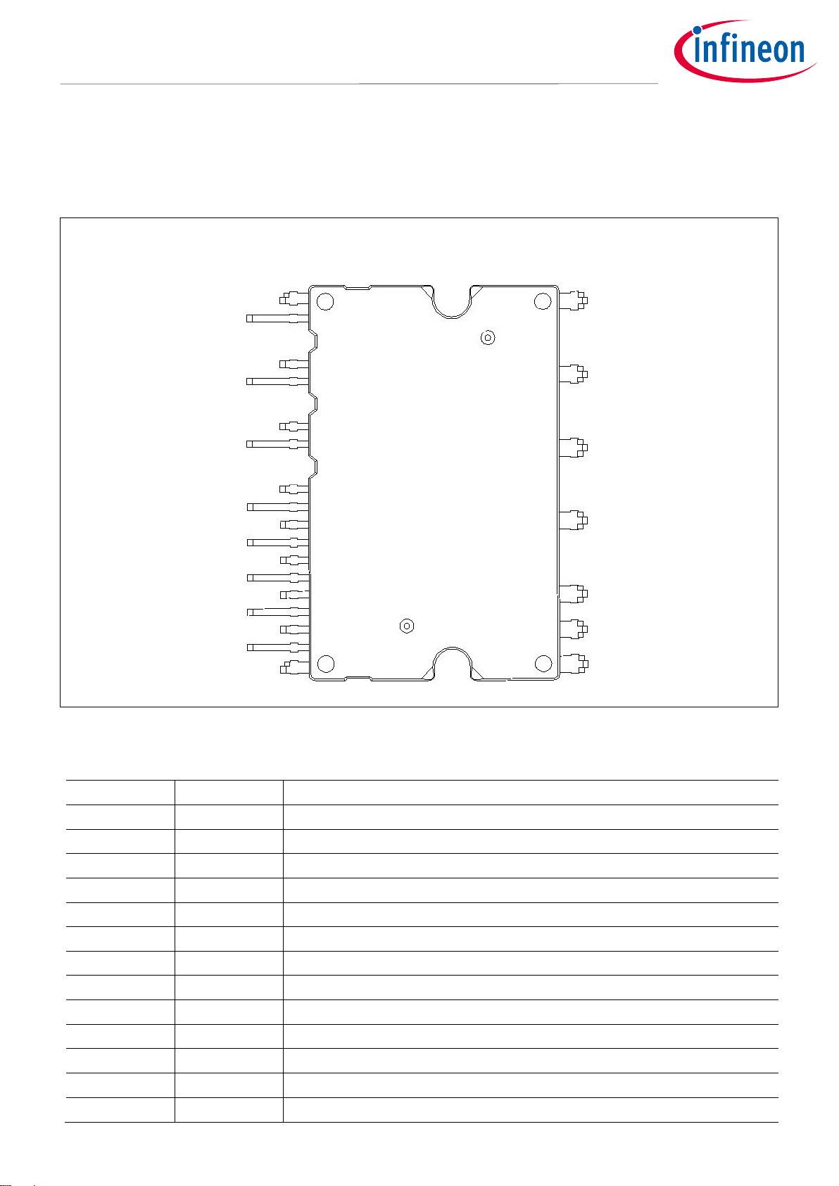
2 Pin Configuration
2.1 Pin Assignment
Bottom View
(1) VS(U)
(2) VB(U)
(3) VS(V)
(4) VB(V)
(5) VS(W)
(6) VB(W)
(7) HIN(U)
(8) HIN(V)
(9) HIN(W)
(10) LIN(U)
(11) LIN(V)
(12) LIN(W)
(13) VDD
(14) RFE
(15) ITRIP
(16) VSS
(24) P
(23) U
(22) V
(21) W
(20) NU
(19) NV
(18) NW
(17) VTH
Figure 2 Module pinout
Table 2 Pin Assignment
Pin Number
Pin name
Pin Description
1
VS(U)
U-phase high side floating IC supply offset voltage
2
VB(U)
U-phase high side floating IC supply voltage
3
VS(V)
V-phase high side floating IC supply offset voltage
4
VB(V)
V-phase high side floating IC supply voltage
5
VS(W)
W-phase high side floating IC supply offset voltage
6
VB(W)
W-phase high side floating IC supply voltage
7
HIN(U)
U-phase high side gate driver input
8
HIN(V)
V-phase high side gate driver input
9
HIN(W)
W-phase high side gate driver input
10
LIN(U)
U-phase low side gate driver input
11
LIN(V)
V-phase low side gate driver input
12
LIN(W)
W-phase low side gate driver input
13
VDD
Low side control supply
Datasheet 5 of 21 V 2.1
2018-08-20
CIPOS™ Maxi IM818
IM818-MCC
Pin Configuration
Pin Number
Pin name
Pin Description
14
RFE
Programmable fault clear time, fault output, enable input
15
ITRIP
Over current shutdown input
16
VSS
Low side control negative supply
17
VTH
Thermistor
18
NW
W-phase low side emitter
19
NV
V-phase low side emitter
20
NU
U-phase low side emitter
21
W
Motor W-phase output
22
V
Motor V-phase output
23
U
Motor U-phase output
24
P
Positive bus input voltage
2.2 Pin Description
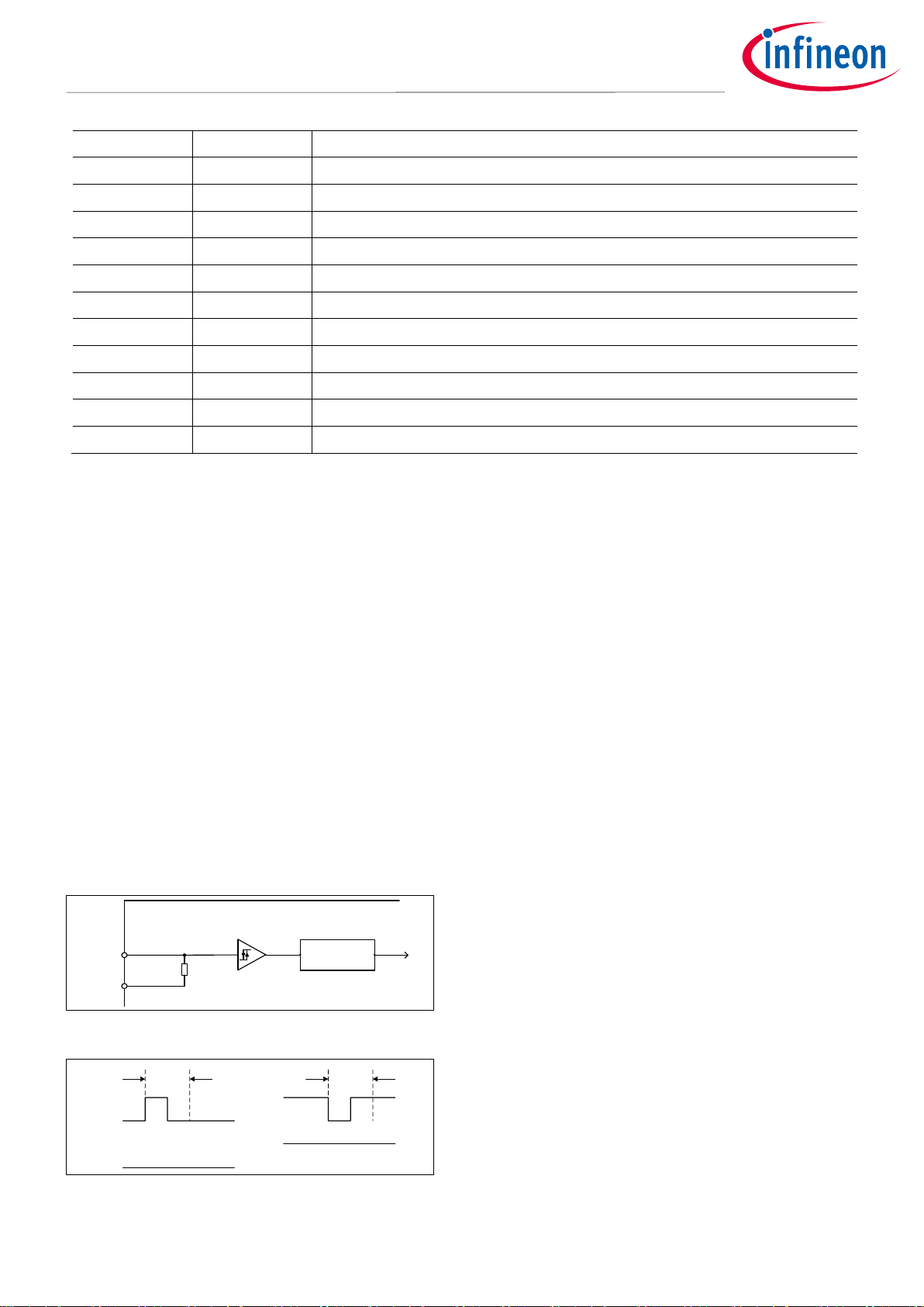
HIN(U, V, W) and LIN(U, V, W) (Low side and high
side control pins, Pin 7 - 12)
These pins are positive logic and they are
responsible for the control of the integrated IGBTs.
The schmitt-trigger input thresholds of them are
such to guarantee LSTTL and CMOS compatibility
down to 3.3 V controller outputs. Pull-down resistor
of about 5 k is internally provided to pre-bias
inputs during supply start-up. Input schmitt-trigger
and noise filter provide beneficial noise rejection to
short input pulses.
The noise filter suppresses control pulses which are
below the filter time t
FIL,IN
. The filter acts according to
Figure 4.
CIPOS
TM
INPUT NOISE
FILTER
k5
Schmitt-Trigger
SWITCH LEVEL
VIH; V
IL
VSS
HINx
LINx
Figure 3 Input pin structure
HIN
LIN
HO
LO
low
high
t
FIL,IN
t
FIL,IN
a) b)
HIN
LIN
HO
LO
Figure 4 Input filter timing diagram
It is not recommended for proper work to provide
input pulse-width lower than 1 µs.
The integrated gate driver provides additionally a
shoot through prevention capability which avoids
the simultaneous on-state of two gate drivers of the
same leg (i.e. HO1 and LO1, HO2 and LO2, HO3 and
LO3). When two inputs of a same leg are activated,
only former activated one is activated so that the leg
is kept steadily in a safe state.
A minimum deadtime insertion of typically 360 ns is
also provided by driver IC, in order to reduce crossconduction of the external power switches.
RFE (Fault / Fault clear time / Enable, Pin 14)
The RFE pin conbines three functions in one pin:
programmable fault clear time by RC-network, faultout and enable input.
The programmable fault-clear time can be adjusted
by RC network, which is external pull-up resistor and
capacitor. For example, typical value is about 1ms at
1 MΩand 2 nF.
The fault-out indicates a module failure in case of
under voltage at pin VDD or in case of triggered over
current detection at ITRIP.
The microcontroller can pull this pin low to disable
the IPM functionality. This is enable function.

Datasheet 6 of 21 V 2.1
2018-08-20
CIPOS™ Maxi IM818
IM818-MCC
Pin Configuration
RFE
VSS
1
R
ON,FLT
From ITRIP - Latch
From UV detection
CIPOS
NOISE FILTER
Schmitt-Trigger
Bi-direction
Figure 5 Internal circuit at pin RFE
VTH (Thermistor, Pin 17)
The VTH pin provides direct access to the NTC,
which is referenced to VSS. An external pull-up
resistor connected to +5 V ensures that the resulting
voltage can be directly connected to the
microcontroller.
ITRIP (Over current detection function, Pin 15)
IM818 provides an over current detection function
by connecting the ITRIP input with the IGBT
collector current feedback. The ITRIP comparator
threshold (typ. 0.5 V) is referenced to VSS ground. An
input noise filter (t
ITRIP
= typ. 500 ns) prevents the
driver to detect false over-current events.
Over current detection generates a shutdown of all
outputs of the gate driver after the shutdown
propagation delay of typically 1µs.
Fault-clear time is set to typical 1.1ms at R
RCIN
= 1 M
Ω and C
RCIN
= 2 nF.
VDD, VSS (Low side control supply and
reference, Pin 13, 16)
VDD is the control supply and it provides power both
to input logic and to output power stage. Input logic
is referenced to VSS ground.
The under-voltage circuit enables the device to
operate at power on when a supply voltage of at
least a typical voltage of V
DDUV+
= 12.2 V is present.
The IC shuts down all the gate drivers power outputs,
when the VDD supply voltage is below V
DDUV-
= 11.2 V.
This prevents the external power switches from
critically low gate voltage levels during on-state and
therefore from excessive power dissipation.
VB(U, V, W) and VS(U, V, W) (High side supplies,
Pin 1 - 6)
VB to VS is the high side supply voltage. The high side
circuit can float with respect to VSS following the
external high side power device emitter voltage.
Due to the low power consumption, the floating
driver stage is supplied by integrated bootstrap
circuit.
The under-voltage detection operates with a rising
supply threshold of typical V
BSUV+
= 11.2 V and a
falling threshold of V
BSUV-
= 10.2 V.
VS(U, V, W) provide a high robustness against
negative voltage in respect of VSS of -50 V transiently.
This ensures very stable designs even under rough
conditions.
NW, NV, NU (Low side emitter, Pin 18 - 20)
The low side emitters are available for current
measurements of each phase leg. It is
recommended to keep the connection to pin VSS as
short as possible in order to avoid unnecessary
inductive voltage drops.
W, V, U (High side emitter and low side collector,
Pin 21 - 23)
These pins are motor U, V, W input pins.
P (Positive bus input voltage, Pin 24)
The high side IGBTs are connected to the bus
voltage. It is noted that the bus voltage does not
exceed 900 V.
Datasheet 7 of 21 V 2.1
2018-08-20
CIPOS™ Maxi IM818
IM818-MCC
Absolute Maximum Ratings
3 Absolute Maximum Ratings
(V
DD
= 15V and TJ = 25°C, if not stated otherwise)
3.1 Module Section
Description
Symbol
Condition
Value
Unit
Storage temperature range
T
STG
-40 ~ 125
°C
Operating case temperature
TC
Refer to Figure 6
-40 ~ 125
°C
Operating junction temperature
TJ -40 ~150
°C
Isolation test voltage
V
ISO
1min, RMS, f = 60Hz
2500
V
3.2 Inverter Section
Description
Symbol
Condition
Value
Unit
Max. blocking voltage
V
CES/VRRM
1200
V
DC link supply voltage of P-N
VPN
Applied between P-N
900
V
DC link supply voltage (surge) of P-N
V
PN(surge)
Applied between P-N
1000
V
DC collector current
IC
TC = 25°C, TJ < 150°C
±16
A
TC = 80°C, TJ < 150°C
±10
Peak collector current
ICP
TC = 25°C, tp < 1 ms
±20
A
Power dissipation per IGBT
P
tot
67.5
W
Short circuit withstand time1
tSC
VDC ≤ 800 V, TJ = 150°C
10
µs
3.3 Control Section
Description
Symbol
Condition
Value
Unit
High Side offset voltage
VS 1200
V
Repetitive peak reverse voltage of
bootstrap diode
V
RRM
1200
V
Module control supply voltage
VDD -1 ~ 20
V
High side floating supply voltage
(VB reference to VS)
VBS -1 ~ 20
V
Input voltage(LIN, HIN, ITRIP, RFE)
VIN -1 ~ VDD + 0.3
V
1
Allowed number of short circuits: < 1000; Time between short circuits: > 1 s.
 Loading...