

INFINEON IM231-M6S1B Datasheet
Final Datashet Please read the Important Notice and Warnings at the end of this document Revision 2.1
www.infineon.com 2019-07-15
IM231-M6S1B / IM231-M6T2B
CIPOS™ Micro IPM 600V/4A
IM231-M6S1B / IM231-M6T2B
Description
IM231-M6-series 3-phase Intelligent Power Modules (IPM) are designed for high-efficiency appliance motor drives
such as air-conditioner fans and refrigerator compressors. These advanced IPMs, available in both surface
mount and through-hole configurations, offer a combination of low V
CE(sat)
TRENCHSTOPTM IGBT6 technology and
the industry benchmark rugged half-bridge drivers. The IPMs have several protection features including precise
overcurrent protection and temperature feedback.
Features
600V 3-phase inverter including gate drivers &
bootstrap function
Low V
CE(sat)
TRENCHSTOP™ IGBT6
Temperature monitor
Accurate overcurrent shutdown (±5%)
Fault reporting and programmable fault clear
Advanced input filter with shoot-through
protection
Optimized dV/dt for loss and EMI trade offs
Open-emitter for single and leg-shunt current
sensing
3.3V logic compatible
Isolation 2000VRMS, 1min
SOP 29x12 DIP 29x12
Potential Applications
Air-conditioner fans
Refrigerator compressors
Ventilation fans & blower fans
Low power motor drives
Product validation
Qualified for industrial applications according to the relevant tests of JEDEC47/20/22.
Table 1 Part Ordering Table
Base Part Number
Package Type
Standard Pack
Orderable Part Number
Form
Quantity
IM231-M6T2B
DIP 29x12
Tube
240
IM231M6T2BAKMA1
IM231-M6S1B
SOP 29x12
Tube
240
IM231M6S1BALMA1
IM231-M6S1B
SOP 29x12
Tape & Reel
500
IM231M6S1BAUMA1

Final Datashet 2 Revision 2.1
2019-07-15
CIPOS™ Micro
IM231-M6S1B / IM231-M6T2B
Table of contents
Table of contents
Description 1
Features 1
Potential Applications ..................................................................................................................... 1
Product validation .......................................................................................................................... 1
Table of contents ............................................................................................................................ 2
1 Internal Electrical Schematic .......................................................................................... 3
2 Pin Configuration........................................................................................................... 4
2.1 Pin Assignment ........................................................................................................................................ 4
2.2 Pin Descriptions....................................................................................................................................... 5
3 Absolute Maximum Rating .............................................................................................. 7
3.1 Module ..................................................................................................................................................... 7
3.2 Inverter .................................................................................................................................................... 7
3.3 Control ..................................................................................................................................................... 7
4 Thermal Characteristics ................................................................................................. 8
5 Recommended Operating Conditions ............................................................................... 9
6 Static Parameters ......................................................................................................... 10
6.1 Inverter .................................................................................................................................................. 10
6.2 Control ................................................................................................................................................... 10
7 Dynamic Parameters ..................................................................................................... 12
7.1 Inverter .................................................................................................................................................. 12
7.2 Control ................................................................................................................................................... 12
8 Thermistor Characteristics ............................................................................................ 13
9 Mechanical Characteristics and Ratings........................................................................... 14
10 Qualification Information .............................................................................................. 15
11 Diagrams & Tables ........................................................................................................ 16
11.1 TC Measurement Point ........................................................................................................................... 16
11.2 Backside Curvature Measurement Points ............................................................................................ 16
11.3 Input-Output Logic Table ...................................................................................................................... 17
11.4 Switching Time Definitions ................................................................................................................... 18
12 Application Guide ......................................................................................................... 19
12.2 TJ vs TTH .................................................................................................................................................. 19
12.3 –VS Immunity ......................................................................................................................................... 20
13 Package Outline ........................................................................................................... 21
13.1 DIP 29x12 ............................................................................................................................................... 21
13.2 SOP 29x12 ............................................................................................................................................. 22
14 Revision History ........................................................................................................... 23

Final Datashet 3 Revision 2.1
2019-07-15
CIPOS™ Micro
IM231-M6S1B / IM231-M6T2B
Internal Electrical Schematic
1 Internal Electrical Schematic
Figure 1 Internal electrical schematic.
Half-Bridge
HVIC
Half-Bridge
HVIC
Half-Bridge
HVIC
1 COM
2 V
B1
3 V
CC1
4 HIN1
5 LIN1
6 RFE
7 V
B2
8 V
CC2
9 HIN2
10 LIN2
11 VTH
12 V
B3
13 V
CC3
14 HIN3
15 LIN3
16 ITRIP
17 V+
18 U/V
S1
19 V
R1
20 V
R2
21 V/V
S2
22 V
R3
23 W/V
S3

Final Datashet 4 Revision 2.1
2019-07-15
CIPOS™ Micro
IM231-M6S1B / IM231-M6T2B
Pin Configuration
2 Pin Configuration
2.1 Pin Assignment
e
1
2
3
4
5
7
8
9
10
12
13
14
15
16
23
22
21
20
19
18
17
11
6
Figure 2 Module pinout
Table 2 Pin Assignment
Pin
Name
Description
1
COM
Logic ground
2
VB1
High side floating supply voltage 1
3
V
DD1
Low side control supply 1
4
HIN1
Logic Input for high side gate driver - Phase 1
5
LIN1
Logic Input for low side gate driver - Phase 1
6
RFE
RCIN / Fault / Enable
7
VB2
High side floating supply voltage 2
8
V
DD2
Low side control supply 2
9
HIN2
Logic input for high side gate driver - Phase 2
10
LIN2
Logic input for low side gate driver - Phase 2
11
VTH
Thermistor output
12
VB3
High side floating supply voltage 3
13
V
DD3
Low side control supply 3
14
HIN3
Logic Input for high side gate driver - Phase 3
15
LIN3
Logic Input for low side gate driver - Phase 3
16
ITRIP
Current protection pin
17
V+
Dc bus voltage positive
18
U/VS1
Output - phase 1, high side floating supply offset 1
19
VR1
Phase 1 low side emitter
20
VR2
Phase 2 low side emitter
21
V/VS2
Output - phase 2, high side floating supply offset 2
22
VR3
Phase 3 low side emitter
23
W/VS3
Output – phase 3, high side floating suppyl offset 3

Final Datashet 5 Revision 2.1
2019-07-15
CIPOS™ Micro
IM231-M6S1B / IM231-M6T2B
Pin Configuration
2.2 Pin Descriptions
HIN(1,2,3) and LIN(1,2,3) (Low side and high side
control pins)
These pins are positive logic and they are
responsible for the control of the integrated IGBT.
The Schmitt-trigger input thresholds of them are
such to guarantee LSTTL and CMOS compatibility
down to 3.3V controller outputs. Pull-down resistor
of about 800k is internally provided to pre-bias
inputs during supply start-up and an ESD diode is
provided for pin protection purposes. Input
Schmitt-trigger and noise filter provide beneficial
noise rejection to short input pulses.
The noise filter suppresses control pulses which are
below the filter time T
FILIN
. The filter acts according
to Figure 4.
CIPOS
TM
INPUT NOISE
FILTER
M8.0
Schmitt-Trigger
SWITCH LEVEL
V
IH
; V
IL
COM
HINx
LINx
Figure 3 Input pin structure
HIN
LIN
HO
LO
low
high
t
FILIN
t
FILIN
a) b)
HIN
LIN
HO
LO
Figure 4 Input filter timing diagram
The integrated gate drive provides additionally a
shoot through prevention capability which avoids
the simultaneous on-state of the high-side and lowside switch of the same inverter phase. A minimum
deadtime insertion of typically 300ns is also
provided by driver IC, in order to reduce crossconduction of the external power switches.
VDD, COM (Low side control supply and reference)
VDD is the control supply and it provides power both
to input logic and to the output power stage. Input
logic is referenced to COM ground.
The under-voltage circuit enables the device to
operate at power on when a supply voltage of at
least a typical voltage of V
DDUV+
= 11.1V is present.
The IC shuts down all the gate drivers power
outputs, when the VDD supply voltage is below V
DDUV-
= 10.9V. This prevents the external power switches
from critically low gate voltage levels during onstate and therefore from excessive power
dissipation.
V
B(1,2,3)
and V
S(1,2,3)
(High side supplies)
VB to VS is the high side supply voltage. The high side
circuit can float with respect to COM following the
external high side power device emitter voltage.
Due to the low power consumption, the floating
driver stage is supplied by integrated bootstrap
circuit.
The under-voltage detection operates with a rising
supply threshold of typical V
BSUV+
= 11.1V and a falling
threshold of V
BSUV-
= 10.9V.
V
S(1,2,3)
provide a high robustness against negative
voltage in respect of COM. This ensures very stable
designs even under rough conditions.
V
R(1,2,3)
(Low side emitters)
The low side emitters are available for current
measurements of each phase leg. It is
recommended to keep the connection to pin COM as
short as possible in order to avoid unnecessary
inductive voltage drops.
VTH (Thermistor output)
A UL certified NTC resistor is integrated in the
module with one terminal of the chip connected to
COM and the other to VTH. When pulled up to a rail
voltage such as VDD or 3.3V by a resistor, the VTH pin
provides an analog voltage signal corresponding to
the temperature of the thermistor.
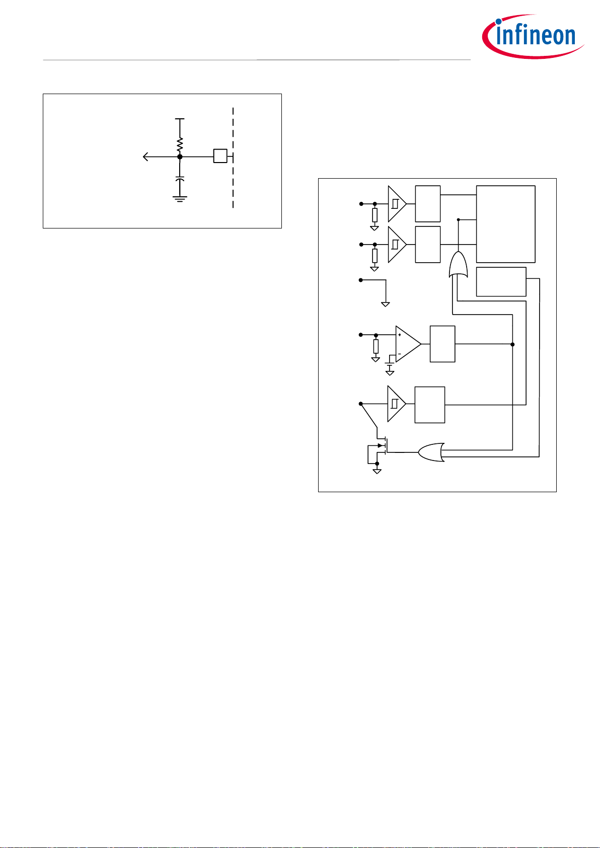
RFE (RCIN / Fault / Enable)
The RFE pin combines 3 functions in one pin: RCIN or
RC-network based programmable fault clear timer,
fault output and enable input.
The RFE pin is normally connected to an RC network
on the PCB per the schematic in Figure 5. Under
normal operating conditions, R
RCIN
pulls the RFE pin
to 3.3V, thus enabling all the functions in the IPM.
The microcontroller can pull this pin low to disable
the IPM functionality. This is is the Enable function.
Final Datashet 6 Revision 2.1
2019-07-15
CIPOS™ Micro
IM231-M6S1B / IM231-M6T2B
Pin Configuration
Figure 5 Typical PCB circuit connected to
the RFE pin
The Fault function allows the IPM to report a Fault
condition to the microncontroller by pulling the RFE
pin low in one of two situations. The first is an undervoltage condition on VDD and the second is when the
ITRIP pin sees a voltage rising above V
IT,TH+
.
The programmable fault clear timer function
provides a means of automatically re-enabling the
module operation a preset amount of time (T
FLT-CLR
)
after the fault condition has disappeared. Figure 6
shows the RFE-related circuit block diagram inside
the IPM.
The length of TFLT-CLR can be determined by using
the formula below.
V
RFE
(t) = 3.3V * (1 – e
-t/RC
)
T
FLT-CLR
= -R
RCIN
* C
RCIN
* ln(1-V
IN,TH+
/3.3V)
For example, if R
RCIN
is 1.2MΩ and C
RCIN
is 1nF, the T
FLT-
CLR
is about 1.7ms with V
IN,TH+
of 2.5V. It is also
important to note that C
RCIN
needs to be minimized in
order to make sure it is fully discharged in case of
over current event.
Since the ITRIP pin has a 500ns input filter, it is
appropriate to ensure that C
RCIN
will be discharged
below V
IN,TH-
by the open-drain MOSFET, after 350ns.
Therefore, the max C
RCIN
can be calculated as:
V
RFE
(t) = 3.3V * e
-t/RC
< V
IN,TH-
C
RCIN
< 500ns / ( - ln (V
IN,TH-
/ 3.3V) * R
RFE_ON
)
Consider V
IN,TH-
of 0.8V and R
RFE_ON
of 50ohm, C
RCIN
should be less than 7nF. It is also suggested to use a
R
RCIN
of between 0.5MΩ and 2MΩ.
Figure 6 RFE internal circuit structure
U/VS1, V/VS2, W/V
S3
(High side emitter and low side
collector)
These pins are motor U, V, W input pins.
V+ (Positive bus input voltage, Pin 23)
The high side IGBTs are connected to the bus
voltage. It is noted that the bus voltage should not
exceed 450V.
Input
Noise
filter
Input
Noise
filter
Deadtime &
Shoot-Through
Prevention
ITRIP
Noise
filter
HIN
LIN
COM
ITRIP
RFE
Noise
filter
VDD
Undervoltage
detection
+3.3V
R
RCIN
C
RCIN
6 RFE
IM231-L6
To Microcontroller

Final Datashet 7 Revision 2.1
2019-07-15
CIPOS™ Micro
IM231-M6S1B / IM231-M6T2B
Absolute Maximum Rating
3 Absolute Maximum Rating
3.1 Module
Table 3
Parameter
Symbol
Condition
Units
Storage temperature
T
STG
-40 ~ 150
°C
Operating case temperature
TC
-40 ~ 125
°C
Operating junction temperature
TJ
-40 ~ 150
°C
Isolation test voltage
V
ISO
1min, RMS, f = 60Hz
2000
V
3.2 Inverter
Table 4
Parameter
Symbol
Condition
Units
Max. blocking voltage
V
CES/VRRM
600
V
Output current
I
O
TC = 25°C 4 A
Peak output current
IOP
TC = 25°C, tp < 1ms
6
A
Peak power dissipation per IGBT
P
tot
TC = 25°C
8.7
W
Short circuit withstand time
T
SC
VDC = 360V, TJ = 150°C, VDD = 15V
Allowed number of short
circuits: <1000, time between
short circuits: >1s
3
μs
3.3 Control
Table 5
Parameter
Symbol
Condition
Units
Low side control supply voltage
V
DD
-0.3 ~ 20
V
Input voltage
V
IN
LIN, HIN, ITRIP, RFE
-0.3 ~ V
DD
V
High side floating supply voltage
(VB reference to VS)
V
BS
-0.3 ~ 20
V

Final Datashet 8 Revision 2.1
2019-07-15
CIPOS™ Micro
IM231-M6S1B / IM231-M6T2B
Thermal Characteristics
4 Thermal Characteristics
Table 6
Parameter
Symbol
Conditions
Min.
Typ.
Max.
Units
Junction-case thermal
resistance, all IGBTs
operating (per module)
R
TH(J-C) _M
-
2.9
3.4
°C/W
Junction-case thermal
resistance, all diodes
operating (per module)
R
TH(J-C)D_M
-
3.0
3.5
°C/W
Single IGBT thermal
resistance, junction-case
R
TH(J-C)
High side V-
phase IGBT
-
10.0
11.6
°C/W
Single diode thermal
resistance, junction-case
R
TH(J-C)D
High side V-
phase IGBT
-
11.2
13.0
°C/W
 Loading...