

INFINEON IM111-X3Q1B Datasheet
Please read the Important Notice and Warnings at the end of this document
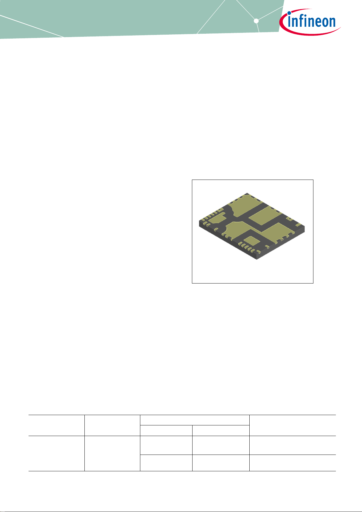
IM111-X3Q1B
CIPOS™ Nano
IM111-X3Q1B
Description
IM111-X3Q1B is an H-bridge integrated power module (IPM) designed for advanced appliance motor drive
applications. This advanced low profile IPM offers a combination of Infineon’s low R
DS(ON)
OptiMOS ™ technology
and the industry benchmark high voltage, rugged driver in a small 12x10mm QFN package.
Features
Integrated gate drivers and bootstrap
functionality
Overcurrent protection & fault reporting
Low 0.063Ω R
DS(on)
, 250V OptiMOS™
Under-voltage lockout for both channels
Shoot through protection
Matched propagation delay for all channels
Optimized dv/dt for loss and EMI trade offs
Advanced input filter
3.3V input logic compatible
Motor power range 80-200W
1500V
RMS
min isolation
Potential Applications
Linear refrigerator compressors
High efficiency single-phase motor drives
DC-AC inverters
Product Validation
Qualified for industrial applications according to the relevant tests of JEDEC47/20/22.
Table 1 Part Ordering Table
Base Part Number
Package Type
Standard Pack
Orderable Part Number
Form
Quantity
IM111-X3Q1B
QFN 12x10mm
Tray
800
IM111-X3Q1B
Tape and Reel
2000
IM111-X3Q1BTR
Final Datasheet
www.infineon.com
Revision 1.0
2019-12-12

CIPOS™ Nano
2
Table of contents
Description ……………………………………………………………………………………………………………..1
Features………………………………………………………………………………………………………………...1
Potential Applications ..................................................................................................................... 1
Product Validation .......................................................................................................................... 1
Table of contents ............................................................................................................................ 2
1
2
2.1
2.2
3
3.1
3.2
3.3
4
5
6
6.1
6.2
7
7.1
7.2
8
9
10
10.1
10.2
11
11.1
11.2
11.3
12
IM111-X3Q1B
Internal Electrical Schematic .......................................................................................... 3
Pin Configuration ........................................................................................................... 4
Pin Assignment ........................................................................................................................................ 4
Pin Descriptions ....................................................................................................................................... 5
Absolute Maximum Rating .............................................................................................. 6
Module ..................................................................................................................................................... 6
Inverter .................................................................................................................................................... 6
Control ..................................................................................................................................................... 6
Thermal Characteristics ................................................................................................. 7
Recommended Operating Conditions ............................................................................... 8
Static Parameters .......................................................................................................... 9
Inverter .................................................................................................................................................... 9
Control ..................................................................................................................................................... 9
Dynamic Parameters ..................................................................................................... 10
Inverter .................................................................................................................................................. 10
Control ................................................................................................................................................... 10
Thermistor Characteristics ............................................................................................ 11
Qualification Information .............................................................................................. 12
Diagrams & Tables ........................................................................................................ 13
Input-Output Logic Table ...................................................................................................................... 13
Switching Time Definitions ................................................................................................................... 13
Application Guide ......................................................................................................... 14
Typical Application Schematic ............................................................................................................. 14
Performance Charts .............................................................................................................................. 14
–Vs Immunity ......................................................................................................................................... 15
Package Outline ........................................................................................................... 16
Revision History ............................................................................................................................ 18
Final Datasheet
Revision 1.0
2019-12-12
CIPOS™ Nano
3
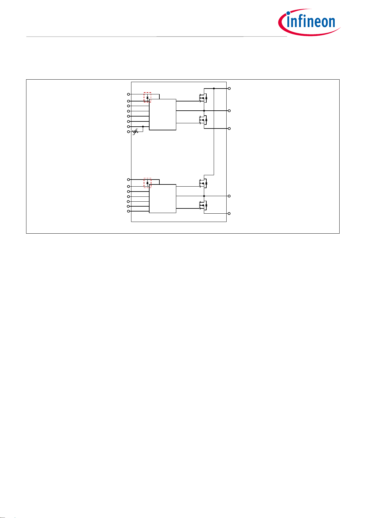
1 Internal Electrical Schematic
Half-Bridge
HVIC
Half-Bridge
HVIC
13 ITRIP1
9 VB1
10 VDD1
11 HIN1
12 LIN1
14 RFE1
15, 39 COM1
16 NTC
36 VB2
37 VDD2
1 HIN2
2 LIN2
5, 38 COM2
6~8, 32~35 V+
19~25 VS1
17~18 VR1
29~30 VR2
26~28, 31 VS2
Integrated in HVIC
3 ITRIP2
4 RFE2
Figure 1 Internal electrical schematic.
IM111-X3Q1B
Final Datasheet
Revision 1.0
2019-12-12
CIPOS™ Nano
4
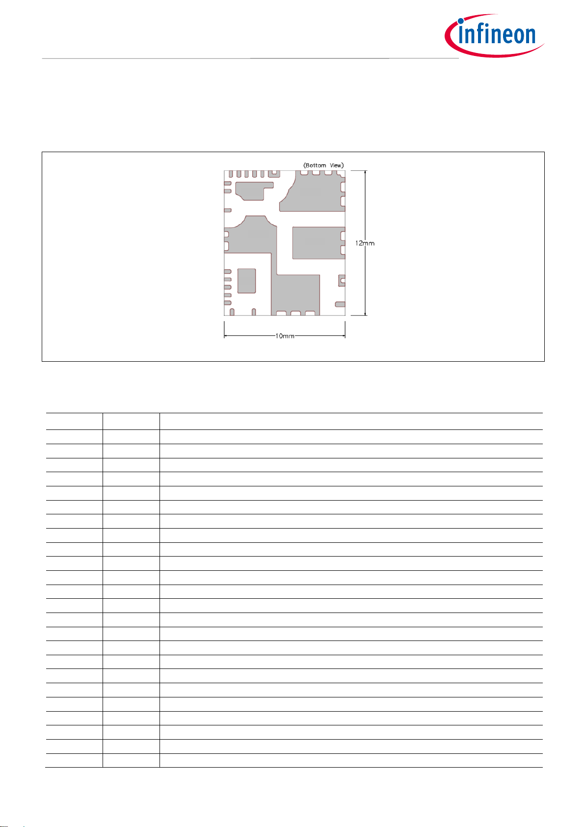
2 Pin Configuration
2.1 Pin Assignment
1
2
3
4
5
6
7
8
9
10
11
12 13 14 15 16 17 18
39
38
19
20 21 22
23
24
25
26
27
28
29
30
31
32333435
3637
Figure 2 Module pinout
Table 2 Pin Assignment
Pin
Name
Description
1
HIN2
Logic Input for High Side Gate Driver (Active High)
2
LIN2
Logic Input for Low Side Gate Driver (Active High)
3
I
TRIP2
Over Current Protection
4
RFE2
Fault Clear, Fault Reporting & Enable
5
COM2
Logic Ground
6-8
V+
DC Bus Voltage Positive
9
VB1
High Side Floating Supply (Bootstrap Cap Connection +)
10
V
DD1
Low Side Control Supply
11
HIN1
Logic Input for High Side Gate Driver (Active High)
12
LIN1
Logic Input for Low Side Gate Driver (Active High)
13
I
TRIP1
Over Current Protection
14
RFE1
Fault Clear, Fault Reporting & Enable
15
COM1
Logic Ground
16
NTC
Negative Temperature Coeffient Thermistor
17-18
VR1
Low Side Source
19-25
VS1
Phase Output
26-28
VS2
Phase Output
29-30
VR2
Low Side Source
31
VS2
Phase Output (Bootstrap Cap Connection -)
32-35
V+
DC Bus Voltage Positive
36
VB2
High Side Floating Supply (Bootstrap Cap Connection +)
37
V
DD2
Low Side Control Supply
38
COM2
Logic Ground
39
COM1
Logic Ground
IM111-X3Q1B
Final Datasheet
Revision 1.0
2019-12-12
CIPOS™ Nano
5
2.2 Pin Descriptions
LIN and HIN (Low side and high side control pins)
These pins are positive logic and they are
responsible for the control of the integrated
OptiMOS. The Schmitt-trigger input thresholds of
them are such to guarantee LSTTL and CMOS
compatibility down to 3.3V controller outputs. Pulldown resistor of about 800k is internally provided
to pre-bias inputs during supply start-up and an ESD
diode is provided for pin protection purposes. Input
Schmitt-trigger and noise filter provide beneficial
noise rejection to short input pulses.
The noise filter suppresses control pulses which are
below the filter time t
FILIN
. The filter acts according to
Figure 4.
CIPOS
TM
INPUT NOISE
FILTER
M8.0
Schmitt-Trigger
SWITCH LEVEL
VIH; V
IL
COM
HINx
LINx
Figure 3 Input pin structure
HIN
LIN
HO
LO
low
high
t
FILIN
t
FILIN
a) b)
HIN
LIN
HO
LO
Figure 4 Input filter timing diagram
The integrated gate drive provides additionally a
shoot through prevention capability which avoids
the simultaneous on-state of the high-side and lowside switch of the same inverter phase. A minimum
deadtime insertion of typically 300ns is also
provided by driver IC, in order to reduce crossconduction of the external power switches.
VDD, COM (Low side control supply and reference)
VDD is the control supply and it provides power both
to input logic and to output power stage. Input logic
is referenced to COM ground.
The under-voltage circuit enables the device to
operate at power on when a supply voltage of at
least a typical voltage of V
DDUV+
= 8.9V is present.
The IC shuts down all the gate drivers power
outputs, when the VDD supply voltage is below V
DDUV-
= 7.7V. This prevents the external power switches
from critically low gate voltage levels during onstate and therefore from excessive power
dissipation.
VB and VS (High side supplies)
VB to VS is the high side supply voltage. The high side
circuit can float with respect to COM following the
external high side power device source voltage.
Due to the low power consumption, the floating
driver stage is supplied by integrated bootstrap
circuit.
The under-voltage detection operates with a rising
supply threshold of typical V
BSUV+
= 8.9V and a falling
threshold of V
BSUV-
= 7.7V.
VS provide a high robustness against negative
voltage in respect of COM. This ensures very stable
designs even under rough conditions.
VR (Low side source)
The low side source is available for current
measurements of each phase leg. It is
recommended to keep the connection to pin COM as
short as possible in order to avoid unnecessary
inductive voltage drops.
VS (High side source and low side drain)
This pin is motor input pin.
V+ (Positive bus input voltage)
The high side OptiMOS devices are connected to the
bus voltage. It is noted that the bus voltage does not
exceed 200V.
I
TRIP
(Over current protection)
Analog input for over-current shutdown. When
active, I
TRIP
shuts down outputs and activates RFE
low.
RFE (Fault clear, fault reporting and enable)
Integrated fault reporting function, fault clear timer
and external enable pin. This pin has negative logic
and an open-drain output.
IM111-X3Q1B
Final Datasheet
Revision 1.0
2019-12-12

CIPOS™ Nano
6
3 Absolute Maximum Ratings
3.1 Module
Table 3
Parameter
Symbol
Condition
Units
Storage temperature
T
STG
-40 ~ 150
°C
Operating case temperature
TC -40 ~ 125
°C
Operating junction temperature
TJ -40 ~ 150
°C
Isolation voltage1
V
ISO
1min, RMS, f = 60Hz
1500
V
1. Characterized, not tested at production
3.2 Inverter
Table 4
Parameter
Symbol
Condition
Units
Max. blocking voltage
V
DSS/VRRM
250
V
Output current based on R
TH(J-C)B
1
IO TC = 25°C, DC
12 A Peak output current
IOP
TC = 25°C, pulsed current
38 A Output current based on R
TH(J-A)
IOA
TA = 25°C, DC
4
A
Peak power dissipation per MOSFET
P TC = 25°C
150
W
1. Limited by wire bonding current capability inside the package
3.3 Control
Table 5
Parameter
Symbol
Condition
Units
Low side control supply voltage
V
DD
-0.3 ~ 20
V
Input voltage LIN, HIN
V
IN
-0.3 ~ V
DD
V
High side floating supply voltage
(VB reference to VS)
V
BS
-0.3 ~ 20
V
IM111-X3Q1B
Final Datasheet
Revision 1.0
2019-12-12
 Loading...