

INFINEON IKW 25N120 Datasheet

IKW25N120T2
TrenchStop
® 2nd
generation Series
Low Loss DuoPack :
• Short circuit withstand time – 10µs
• Designed for :
- Frequency Converters
- Uninterrupted Power Supply
• TrenchStop
- very tight parameter distribution
- high ruggedness, temperature stable behavior
• Easy paralleling capability due to positive temperature coefficient
in V
CE(sat)
• Low EMI
• Low Gate Charge
• Very soft, fast recovery anti-parallel EmCon HE diode
• Qualified according to JEDEC
• Pb-free lead plating; RoHS compliant
Complete product spectrum and PSpice Models : http://www.infineon.com/igbt/
Type V
® 2nd
generation for 1200 V applications offers :
CE
IGBT in 2nd generation TrenchStop®
with soft, fast recovery anti-parallel EmCon diode
1
for target applications
IC V
CE(sat),Tj=25°C
T
Marking Code Package
j,max
C
G
PG-TO-247-3
E
IKW25N120T2 1200V 25A 1.7V
175°C
K25T1202 PG-TO-247-3
Maximum Ratings
Parameter Symbol Value Unit
Collector-emitter voltage VCE 1200 V
DC collector current (Tj=150°C)
= 25°C
T
C
= 110°C
T
C
Pulsed collector current, tp limited by T
I
jmax
Turn off safe operating area
≤ 1200V, Tj ≤ 175°C
V
CE
Diode forward current (Tj=150°C)
= 25°C
T
C
= 110°C
T
C
Diode pulsed current, tp limited by T
I
jmax
Gate-emitter voltage VGE
Short circuit withstand time2)
VGE = 15V, V
≤ 600V, T
CC
j, start
≤ 175°C
Power dissipation
= 25°C
T
C
Operating junction temperature Tj -40...+175
Storage temperature T
Soldering temperature, 1.6mm (0.063 in.) from case for 10s
I
C
50
A
25
100
Cpuls
-
100
I
F
40
25
100
Fpuls
±20
t
10
SC
P
349 W
tot
V
µs
°C
-55...+150
stg
- 260
Wavesoldering only, temperature on leads only
1
J-STD-020 and JESD-022
2)
Allowed number of short circuits: <1000; time between short circuits: >1s.
Power Semiconductors
1 Rev. 2.1 Sep 08

IKW25N120T2
TrenchStop
® 2nd
generation Series
Thermal Resistance
Parameter Symbol Conditions Max. Value Unit
Characteristic
IGBT thermal resistance,
junction – case
Diode thermal resistance,
R
0.43
thJC
R
0.81
thJCD
K/W
junction – case
Thermal resistance,
R
40
thJA
junction – ambient
Electrical Characteristic, at T
Parameter Symbol Conditions
= 25 °C, unless otherwise specified
j
Value
Unit
min. typ. max.
Static Characteristic
Collector-emitter breakdown voltage V
Collector-emitter saturation voltage V
Diode forward voltage
Gate-emitter threshold voltage V
Zero gate voltage collector current I
Gate-emitter leakage current I
(BR)CESVGE
VGE = 15V, IC=25A
CE(sat)
VF VGE=0V, IF=25A
IC=1.0mA,VCE=V
GE(th)
CES
VCE=0V,VGE=20V - - 200 nA
GES
=0V, IC=500µA 1200 - -
=25°C
T
j
=150°C
T
j
=175°C
T
j
=25°C
T
j
=150°C
T
j
=175°C
T
j
V
=1200V,
CE
VGE=0V
=25°C
T
j
T
=150°C
j
T
=175°C
j
-
-
-
-
-
-
5.2 5.8 6.4
GE
-
-
1.7
2.1
2.2
1.65
1.7
1.65
-
-
2.2
2.2
0.4
4.0
20
V
-
-
-
-
mA
Transconductance gfs VCE=20V, IC=25A - 13.5 - S
Power Semiconductors
2 Rev. 2.1 Sep 08

IKW25N120T2
TrenchStop
® 2nd
generation Series
Dynamic Characteristic
Input capacitance C
Output capacitance C
Reverse transfer capacitance C
Gate charge Q
Internal emitter inductance
- 1600 -
iss
- 155 -
oss
rss
VCC=960V, IC=40A
Gate
=25V,
V
CE
V
=0V,
GE
f=1MHz
V
=15V
GE
pF
- 90 -
- 120 - nC
LE - 13 - nH
measured 5mm (0.197 in.) from case
Short circuit collector current1) I
C(SC)
V
GE
V
CC
T
j,start
T
j,start
=15V,t
= 600V,
SC
= 25°C
= 175°C
≤10µs
-
150
115
- A
Switching Characteristic, Inductive Load, at T
Parameter Symbol Conditions
=25 °C
j
Value
Unit
min. typ. max.
IGBT Characteristic
Turn-on delay time t
Rise time tr - 20 -
Turn-off delay time t
Fall time tf - 95 -
Turn-on energy Eon - 1.55 -
Turn-off energy E
Total switching energy Ets
- 27 -
T
d(on)
- 265 -
d(off)
=25°C,
j
V
=600V,IC=25A,
CC
V
=0/15V,
GE
=16.4Ω,
R
G
2)
L
=105nH,
σ
2)
=39pF
C
σ
Energy losses include
- 1.35 -
off
“tail” and diode
reverse recovery.
- 2.9 -
ns
mJ
Anti-Parallel Diode Characteristic
Diode reverse recovery time t
Diode reverse recovery charge Qrr - 2.05 µC
Diode peak reverse recovery current I
Diode peak rate of fall of reverse
recovery current during t
b
- 195 - ns
rr
- 20 A
rrm
/dt
di
rr
T
=25°C,
j
=600V, IF=25A,
V
R
/dt=1050A/µs
di
F
- 475 -
A/µs
1)
Allowed number of short circuits: <1000; time between short circuits: >1s.
2)
Leakage inductance L
Power Semiconductors
and Stray capacity Cσ due to dynamic test circuit in Figure E.
σ
3 Rev. 2.1 Sep 08

IKW25N120T2
TrenchStop
® 2nd
generation Series
Switching Characteristic, Inductive Load, at T
Parameter Symbol Conditions
=175 °C
j
Value
Unit
min. typ. max.
IGBT Characteristic
Turn-on delay time t
Rise time tr - 24 -
Turn-off delay time t
Fall time tf - 164 -
Turn-on energy Eon - 2.25 -
Turn-off energy E
Total switching energy Ets
- 25 -
T
d(on)
- 340 -
d(off)
=175°C
j
V
=600V,IC=25A,
CC
V
=0/15V,
GE
R
= 16.4Ω,
G
1)
=175nH,
L
σ
1)
=67pF
C
σ
Energy losses include
- 2.05 -
off
“tail” and diode
reverse recovery.
- 4.3 -
ns
mJ
Anti-Parallel Diode Characteristic
Diode reverse recovery time t
Diode reverse recovery charge Qrr - 3.65 - µC
Diode peak reverse recovery current I
Diode peak rate of fall of reverse
recovery current during t
b
- 290 - ns
rr
- 24 - A
rrm
/dt
di
rr
T
=175°C
j
=600V, IF=25A,
V
R
/dt=1000A/µs
di
F
- 330
A/µs
1)
Leakage inductance L
and Stray capacity Cσ due to dynamic test circuit in Figure E.
σ
Power Semiconductors
4 Rev. 2.1 Sep 08
IKW25N120T2
TrenchStop
® 2nd
generation Series
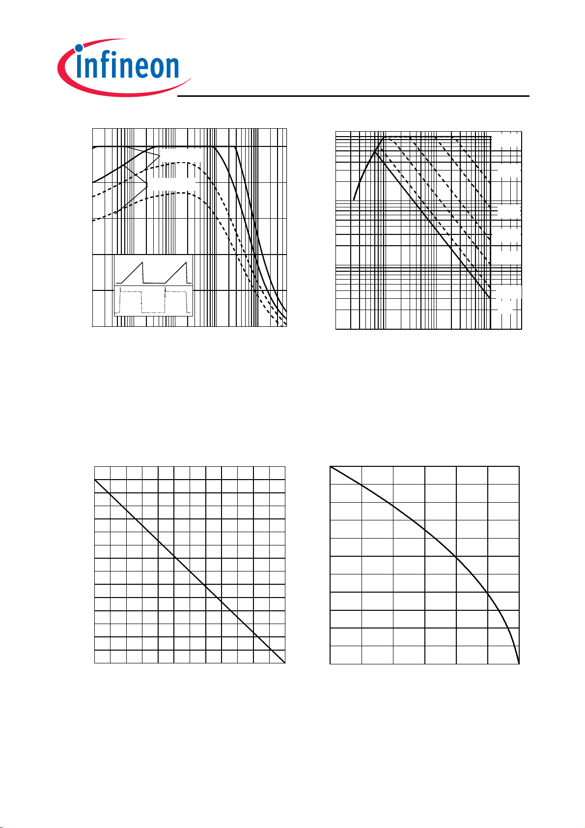
00A
TC=80°C
80A
60A
40A
, COLLECTOR CURRENT
C
I
20A
0A
10Hz 100Hz 1kHz 10kHz 100kHz
TC=110°C
I
c
I
c
f, SWITCHING FREQUENCY
Figure 1. Collector current as a function of
switching frequency
≤ 175°C, D = 0.5, V
(T
j
= 0/+15V, R
V
GE
= 12Ω)
G
= 600V,
CE
100A
10A
1A
, COLLECTOR CURRENT
C
I
0.1A
1V 10V 100V 1000V
VCE, COLLECTOR-EMITTER VOLTAGE
Figure 2. Safe operating area
(D = 0, T
≤175°C;V
T
j
= 25°C,
C
GE
tp=3µs
10µs
50µs
150µs
500µs
20ms
DC
=15V)
50W
00W
50W
00W
150W
, POWER DISSIPATION
tot
100W
P
50W
0W
25°C 50°C 75°C 100°C 125°C 150°C
50A
40A
30A
20A
, COLLECTOR CURRENT
C
I
10A
0A
25°C 75°C 125°C
TC, CASE TEMPERATURE TC, CASE TEMPERATURE
Figure 3. Maximum power dissipation as a
function of case temperature
≤ 175°C)
(T
j
Figure 4. Maximum collector current as a
function of case temperature
(V
≥ 15V, Tj ≤ 175°C)
GE
Power Semiconductors
5 Rev. 2.1 Sep 08
 Loading...