

Technische Information / technical information
IGBT-Module
IGBT-modules
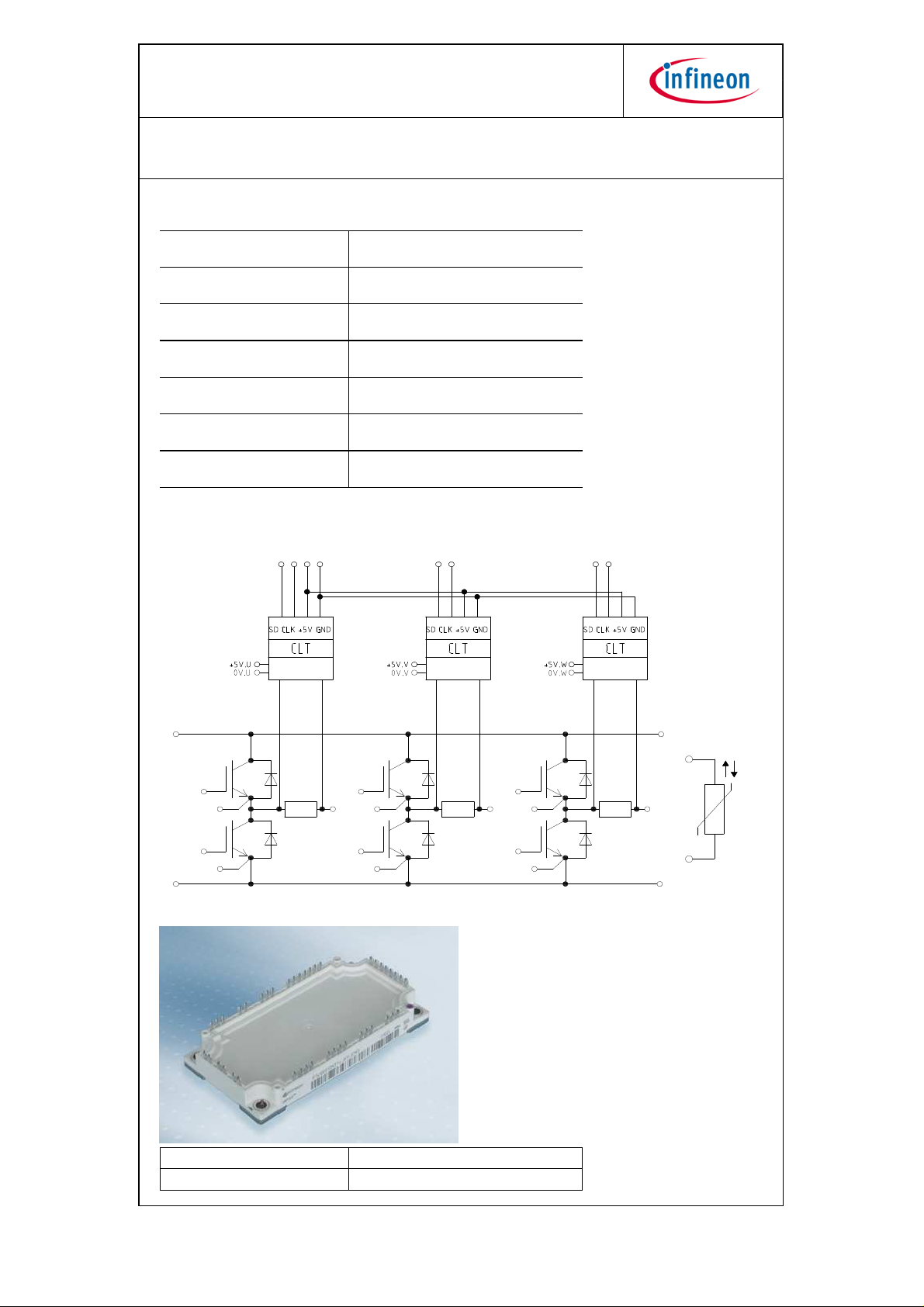
MIPAQ™ sense Modul in Sixpack-Konfiguration mit Trench/Feldstopp IGBT4, Emitter Controlled 4 Diode und Strommesswiderstand mit integriertem Σ/∆-Wandler und galvanisch getrennter digitalen Schnittstelle
MIPAQ™ sense module in Sixpack-configuration with trench/fieldstop IGBT4, emitter controlled 4 diode and current sense shunt
with integrated Σ/∆-converter and galvanical isolation of the digital interface
Kenndaten
key data
Topologie
topology
Halbleiter-Nenndaten
rated semiconductor data
IFS75S12N3T4_B11
B6I
1200V, 75A
Art der Belastung
load type
Zielanwendung
target application
Sensoren
sensors
Digitale Schnittstelle
digital interface
Normen
standards
Blockschaltbild
block diagram
ohmsch-induktiv
resistive-inductive
Industrieantriebe, USV, Klimatisierungsgeräte, Solarumrichter
industrial drives, UPS, Air conditioning, Solar inverters
Strommesswiderstände für Laststrom, NTC für
Bodenplattentemperatur
shunts for output current, NTC for baseplate temperature
5V-CMOS, galvanische Trennung nach IEC61800-5-1
5V-CMOS, galvanic isolation according to IEC61800-5-1
IEC61800-5-1 (Overvoltage Category III, Polution Degree 2,
Insulating Material Groupe II), UL94, RoHs
σ/δ σ/δ σ/δ
Foto
photo
prepared by: US date of publication: 16.08.2011
approved by: MH revision: 2.1
ϑ
1(13)
DB_IFS75S12N3T4_B11_2V1_2011-08-16
Technische Information / technical information
Gate-Emitter Reststrom
IGBT-Module
IGBT-modules
IGBT-Wechselrichter / IGBT-inverter
Höchstzulässige Werte / maximum rated values
Kollektor-Emitter-Sperrspannung
collector-emitter voltage
Kollektor-Dauergleichstrom
DC-collector current
Periodischer Kollektor Spitzenstrom
repetitive peak collector current
Gesamt-Verlustleistung
total power dissipation
Gate-Emitter-Spitzenspannung
gate-emitter peak voltage
IFS75S12N3T4_B11
Tvj = 25°C V
TC = 95°C, Tvj = 175°C I
tP = 1 ms I
TC = 25°C, Tvj = 175°C P
Zieldaten / target data
1200 V
75 A
150 A
349 W
+/-20 V
C,nom
V
CES
CRM
tot
GES
Charakteristische Werte / characteristic values
Kollektor-Emitter Sättigungsspannung
collector-emitter saturation voltage
Gate-Schwellenspannung
gate threshold voltage
Gateladung
gate charge
Interner Gatewiderstand
internal gate resistor
Eingangskapazität
input capacitance
Rückwirkungskapazität
reverse transfer capacitance
Kollektor-Emitter Reststrom
collector-emitter cut-off current
gate-emitter leakage current
Einschaltverzögerungszeit (ind. Last)
turn-on delay time (inductive load)
Anstiegszeit (induktive Last)
rise time (inductive load)
Abschaltverzögerungszeit (ind. Last)
turn-off delay time (inductive load)
Fallzeit (induktive Last)
fall time (inductive load)
Einschaltverlustenergie pro Puls
turn-on energy loss per pulse
Abschaltverlustenergie pro Puls
turn-off energy loss per pulse
Kurzschlußverhalten
SC Data
Innerer Wärmewiderstand
thermal resistance, junction to case
Übergangs-Wärmewiderstand
thermal resistance, case to heatsink
IC = 75 A, VGE = 15 V, Tvj = 25°C
IC = 75 A, VGE = 15 V, Tvj = 125°C
IC = 75 A, VGE = 15 V, Tvj = 150°C
IC = 4,00 mA, VCE = VGE, Tvj = 25°C V
VGE = -15 V ... +15 V Q
Tvj = 25°C R
f = 1 MHz,Tvj = 25 °C,VCE = 25 V, VGE = 0 V C
f = 1 MHz, Tvj = 25 °C,VCE = 25 V, VGE = 0 V C
VCE = 1200 V, VGE = 0 V, Tvj = 25 °C I
VCE = 0 V, VGE = 20 V, Tvj = 25°C I
IC = 75 A, VCE = 600 V Tvj = 25°C
VGE = ±15 V Tvj =125°C t
R
= 2,2 Ω Tvj =150°C
Gon
IC = 75 A, VCE = 600 V Tvj = 25°C
VGE = ±15 V Tvj =125°C t
R
= 2,2 Ω Tvj =150°C
Gon
IC = 75 A, VCE = 600 V Tvj = 25°C
VGE = ±15 V Tvj =125°C t
R
= 2,2 Ω Tvj =150°C
Goff
IC = 75 A, VCE = 600 V Tvj = 25°C
VGE = ±15 V Tvj =125°C t
R
= 2,2 Ω Tvj =150°C
Goff
IC = 75 A, VCE = 600 V Tvj = 25°C
VGE = ±15 V, diC/dt = 2,4 kA/µs (Tvj =150°C) Tvj =125°C E
R
= 2,2 Ω Tvj =150°C
Goff
IC = 75 A, VCE = 600 V Tvj = 25°C
VGE = ±15 V, duCE/dt = 3,3 kV/µs (Tvj =150°C) Tvj =125°C E
R
= 2,2 Ω Tvj =150°C
Goff
VGE ≤ 15 V, VCC = 800 V
V
CEmax=VCES -LsCE
pro IGBT / per IGBT
pro IGBT / per IGBT
λ
= 1 W/(m*K) / λ
Paste
·di/dt, tP ≤ 10 µs, Tvj ≤ 150°C
= 1 W/(m*K)
grease
min. typ. max.
V
CE sat
5,2 5,8 6,4 V
GE(th)
G
Gint
ies
res
CES
GES
d,on
r
d,off
f
on
off
I
SC
R
thJC
R
thCH
1,85 2,15 V
2,15 V
2,25 V
0,57 µC
10
4,30 nF
0,16 nF
1,0 mA
100 nA
0,135 µs
0,15 µs
0,152 µs
0,036 µs
0,042 µs
0,045 µs
0,33 µs
0,38 µs
0,42 µs
0,108 µs
0,190 µs
0,222 µs
4,87 mJ
7,7 mJ
8,92 mJ
4,76 mJ
7,16 mJ
7,95 mJ
270
0,43
K/W
0,195 K/W
Ω
A
prepared by: US date of publication: 16.08.2011
approved by: MH revision: 2.1
2(13)
DB_IFS75S12N3T4_B11_2V1_2011-08-16
Technische Information / technical information
pro Diode / per diode
IGBT-Module
IGBT-modules
Diode-Wechselrichter / diode-inverter
Höchstzulässige Werte / maximum rated values
Periodische Spitzensperrspannung
repetitive peak reverse voltage
Dauergleichstrom
DC forward current
Periodischer Spitzenstrom
repetitive peak forw. current
Grenzlastintegral
I2t - value
Spitzenverlustleistung
maximum power dissipation
IFS75S12N3T4_B11
Tvj = 25°C V
tP = 1 ms I
VR = 0V, tP = 10ms, Tvj = 125°C
VR = 0V, tP = 10ms, Tvj = 150°C
TC = 25°C, Tvj = 175°C P
Zieldaten
Target Data
RRM
I
F
FRM
I2t
RQM
1200 V
75 A
150 A
960
960
217 W
A²s
A²s
Charakteristische Werte / characteristic values
Durchlaßspannung
forward voltage
Rückstromspitze
peak reverse recovery current
Sperrverzögerungsladung
recovered charge
Abschaltenergie pro Puls
reverse recovery energy
Innerer Wärmewiderstand
thermal resistance, junction to case
Übergangs-Wärmewiderstand
thermal resistance, case to heatsink
IF = 75 A, VGE = 0V Tvj = 25°C
IF = 75 A, VGE = 0V Tvj=125°C V
IF = 75 A, VGE = 0V Tvj=150°C
IF = 75 A, - diF/dt = 2,9 kA/µs (Tvj = 150°C) Tvj = 25°C
VR = 600V Tvj = 125°C I
VGE = -15V Tvj=150°C
IF = 75 A, - diF/dt = 2,9 kA/µs (Tvj = 150°C) Tvj = 25°C
VR = 600V Tvj = 125°C Q
VGE = -15V Tvj =150°C
IF =75 A, - diF/dt = 2,9 kA/µs (Tvj = 150°C) Tvj = 25°C
VR = 600V Tvj = 125°C E
VGE = -15V Tvj =150°C
pro Diode / per diode
λ
= 1 W/(m*K) / λ
Paste
Strommesswiderstand / shunt
Charakteristische Werte / characteristic values
Nennwiderstand
rated resistance
Temperaturkoeffizient
temperature coefficient (tcr)
Betriebstemperatur Strommesswiderstand
operation temperature shunt
Innerer Wärmewiderstand;
thermal resistance; junction to case
25°C < T
20°C - 60°C
= 1 W/(m*K)
grease
< 200°C R
shunt
min. typ. max.
F
RM
r
rec
R
thJC
R
thCH
min. typ. max.
2,376 2,40 2,424
25
ϑ
CR
T
vjop
R
thJC
1,70 2,15 V
1,65 V
1,65 V
91 A
98 A
105 A
8,2 µC
13,8 µC
15,5 µC
4,8 mJ
6,9 mJ
7,7 mJ
0,69
0,31 K/W
< 30 ppm/K
13,0 K/W
K/W
mΩ
200 °C
prepared by: US date of publication: 16.08.2011
approved by: MH revision: 2.1
3(13)
DB_IFS75S12N3T4_B11_2V1_2011-08-16
Technische Information / technical information
Material für innere Isolation
thermal resistance, case to heatsink
λ
Paste
= 1 W/(m*K) /
λ
grease
= 1 W/(m*K)
Höchstzulässige Sperrschichttemperatur
Temperatur im Schaltbetrieb
Zulässige Gehäuse-Betriebstemperatur
Anzugsdrehmoment f. mech. Befestigung
IGBT-Module
IGBT-Modules
NTC-Widerstand / NTC-thermistor
Charakteristische Werte / characteristic values min. typ. max.
Nennwiderstand
rated resistance
Abweichung von R
deviation of R
Verlustleistung
power dissipation
B-Wert
B-value
B-Wert
B-value
B-Wert
B-value
Angaben gemäß gültiger Application Note.
Specification according to the valid application note.
100
100
IFS75S12N3T4_B11
TC = 25°C R
TC = 100°C, R
TC = 25°C P
R2 = R25 exp [B(1/T2 - 1/(298,15K))] B
R2 = R25 exp [B(1/T2 - 1/(298,15K))] B
R2 = R25 exp [B(1/T2 - 1/(298,15K))] B
100
= 493 Ω
Zieldaten
Target Data
25
-5 5 %
∆R/R
25
25/50
25/80
25/100
5,00
20,0 mW
3375 K
3411 K
3433 K
kΩ
Modul / module
Isolations-Prüfspannung
insulation test voltage
Material Modulgrundplatte
material of module baseplate
material for internal insulation
Kriechstrecke
creepage distance
Luftstrecke
clearance
Vergleichszahl der Kriechwegbildung
comperative tracking index
Übergangs-Wärmewiderstand
Modulinduktivität
stray inductance module
Modulleitungswiderstand, Anschlüsse - Chip
module lead resistance, terminals - chip
maximum junction temperature
temperature under switching conditions
allowed operation case temperature
Lagertemperatur
storage temperature
mounting torque
Gewicht
weight
RMS, f = 50 Hz, t = 1 min
Kontakt - Kühlkörper / Kontakt - Kontakt
terminal to heatsink / terminal to terminal
Kontakt - Kühlkörper / Kontakt - Kontakt
terminal to heatsink / terminal to terminal
pro Modul / per module
TC = 25°C, pro Schalter / per switch
(Rshunt ist inklusive / Rshunt is inclusiv)
Wechselrichter
inverter
Wechselrichter
inverter
Bodenplatte / Kontakt
base plate / contact
Schraube M5 - Montage gem. gültiger Applikation Note
screw M5 - mounting according to valid application note
min. typ. max.
V
ISOL
d
creepage
d
clearance
CTI > 200
2,5 kV
CU
Al2O
3
10 mm
7,5 mm
min. typ. max.
R
thCH
L
sCE
R
CC´+EE´
T
vj max
T
vj op
T
c op
T
stg
M 3,00 - 6,00 Nm
G 316 g
0,011 K/W
22 nH
1,2
175 °C
-40 150 °C
-40 125 °C
-40 125 °C
mΩ
prepared by: US date of publication: 16.08.2011
approved by: MH revision: 2.1
4(13)
DB_IFS75S12N3T4_B11_2V1_2011-08-16

Technische Information / technical information
M,max,high_res
output current
) and ∆PDM
PDM
DC_offset
DC offset drift due to temperature from shunt to Pin
PDM
DC_offset,Vdd1
IGBT-Module
IGBT-Modules
Sigma-Delta-Wandlereinheit / sigma-delta converter unit
Charakteristische Werte / characteristic values
V
= 4.75 V bis / to 5.25 V, V
cc1
Maximale Phasenstromfrequenz
maximum line current frequency
Maximale periodische Isolationsspannung I
maximum repetive isolation voltage I
Maximale periodische Isolationsspannung II
maximum repetive isolation voltage II
Spannungsflankensteilheitsfestigkeit
voltage slope immunity
Höchste zulässige Überspannung
highest allowable overvoltage
Maximale Stoßisolationsspannung
maximum surge isolation voltage
Isolationswiderstand
isolation resistance
Maximaler Wechselrichterausgangsstrom für
höchstmögliche Auflösung
maximum inverter output current for highest
resolution
Maximaler Wechselrichterausgangsstrom für
lineares Wandlerverhalten
maximum inverter output current for linear
converter behavior
Tastverhältnis des Ausganges SD bei 0 A
Wechselrichterausgangsstrom
duty cycle of output SD at 0 A inverter output
current
Tastverhältnis des Ausganges SD bei max.
positivem Wechselrichterausgangsstrom
duty cycle of output SD at max. positive inverter
output current
Tastverhältnis des Ausganges SD bei max.
negativem Wechselrichterausgangsstrom
duty cycle of output SD at max. negative inverter
output current
Differentieller Verstärkungsfehler
differential gain error
Gleichstrom-Versatz vom Strommesswiderstand
zum Ausgang SD
DC offset from internal shunt to Pin SD
Temperaturdrift des Gleichstrom-Versatz vom
Strommesswiderstand zum Ausgang SD
SD
Versorgungsspannungsdrift (V
Versatz vom Strommesswiderstand zum Ausgang
SD
DC Offset drift due to V
Effektive Anzahl der Bits (ENOB Auflösung)
effective number of bits (ENOB resolution)
Signal-Rausch-Abstand
signal-to-noise ratio
Gesamtklirrfaktor
total harmonic disortion
1)
= Erklärung von PDM%: 100% = alle Pulse sind ‘1’, 0% = alle Pulse sind ’0’, 50% = 50% für jeweils ‘1’ and ‘0’ am Ausgangs-Pin SD.
1)
= explanation of PDM%: 100% = all ‘1’, 0% = all’0’, 50% = 50% for both ‘1’ and ‘0’ at output pin SD.
= 4.5 V bis / to 5.5 V, TC = 105°C sofern nicht anders spezifiziert / unless otherwise noted.
cc2
) des Gleichstrom-
dd1
from shunt to Pin SD
dd1
IFS75S12N3T4_B11
Phase / phase U, V, W
Logik (SD/CLK) gegen Lastausgänge
logik (SD/CLK) to terminals
Leistungshalbleiter gegen Bodenplatte (f = 50Hz, t = 1min)
power semiconductor to base plate (f = 50Hz, t = 1min)
V
= 500V zwschen GND und 0V.U, 0V.V bzw. 0V.W
IMV
V
= 500V between GND and 0V.U, 0V.V, 0V.W, respectively
IMV
Zwischen GND und 0V.U, 0V.V bzw. 0V.W
Between GND and 0V.U, 0V.V, 0V.W, respectively
Zwischen GND und 0V.U, 0V.V bzw. 0V.W
Between GND and 0V.U, 0V.V, 0V.W, respectively
V
= 500V zwschen GND und 0V.U, 0V.V bzw. 0V.W
IMV
V
= 500V between GND and 0V.U, 0V.V, 0V.W, respectively
IMV
Phase / phase U, V, W
Phase / phase U, V, W
TC = 25 °C; IM = 0 A; Phase / phase U, V, W PDM
TC = 25 °C; IM > 133,3 A; Phase / phase U, V, W PDM
TC = 25 °C; IM < -133,3A; Phase / phase U, V, W PDM
Bedingung: Shunt-Spannungsabfall bis Pin SD
conditions: shunt voltage drop to Pin SD
Bedingung: IM = 0A, siehe auch Diagramme ΔPDM = f(Ta) und
∆PDM = f(V
conditions: IM = 0A, see also diagrams ∆PDM = f(T
= f(V
Bedingung: IM = 0A, siehe Diagramm ∆PDM = f(Ta)
conditions: IM = 0A, see diagram ∆PDM = f(Ta)
Bedingung: IM = 0A, siehe Diagramm ∆PDM = f(V
conditions: IM = 0A, see diagram ∆PDM = f(V
Phase U, V, W Bedingungen: IM = [-83,3A; +83,3A], f(IM) =
1kHz, siehe Diagramm ENOB = f(Ta)
phase U, V, W conditions: IM = [-83,3A; +83,3A], f(IM) = 1kHz,
see diagram ENOB = f(Ta)
Phase U, V, W Bedingungen: IM = [-83,3A; +83,3A], f(IM) =
1kHz, siehe Diagramm SNR = f(Ta)
phase U, V, W conditions: IM = [-83,3A; +83,3A], f(IM) = 1kHz,
see diagram SNR = f(Ta)
Phase U, V, W Bedingungen: IM = [-83,3A; +83,3A], f(IM) =
1kHz, siehe Diagramm THD = f(Ta)
phase U, V, W conditions: IM = [-83,3A; +83,3A], f(IM) = 1kHz,
see diagram THD = f(Ta)
)
CC1
)
CC1
a
)
CC1
)
CC1
V
d/dt V
V
V
I
I
M,max,linear
PDM
ENOB 10 12 bit
SNR 65 74 dB
f
SYS
V
iorm
ISOL
slope
IOTM
ISOM
R
IO
Izero
Ipos
Ineg
G -1,56 - 1,56 %
DC_offset,Ta
THD 65 72 dB
Zieldaten
Target Data
min. typ. max.
30,0 kHz
1420 V
2500 V
50 kV/µs
6000 V
6000 V
1 GΩ
-133,3 - +133,3 A
-83,3 - +133,3 A
49,6 50,0 50,4 %
100,0 %
0,0 %
- - 0,4
0,09 - 0,135
0,116 - 0,15
1)
1)
1)
1)
%
PDM
1)
%
PDM
1)
%
PDM
prepared by: US date of publication: 16.08.2011
approved by: MH revision: 2.1
5(13)
DB_IFS75S12N3T4_B11_2V1_2011-08-16

Technische Information / technical information
Maximaler Stromverbrauch Leistungsteil
Maximaler Stromverbrauch Logikteil
Ausgangsspannung High-Pegel: SD
IGBT-Module
IGBT-Modules
Versorgungsspannung Shuntseite
supply voltage shunt side
Versorgungsspannung Logikteil
supply voltage logic section
maximal current consumption power section
maximal current consumption logic section
V
Unterspannungserkennungsschwelle
CC1U,V,W
V
undervoltage detection threshold
CC1U,V,W
V
Unterspannungserkennungsschwelle
CC1U,V,W
V
undervoltage detection threshold
CC1U,V,W
Hysteresis (V
hystresis (V
V
Unterspannungserkennungsschwelle
CC2
V
undervoltage detection
CC2
V
Unterspannungserkennungsschwelle
CC2
V
undervoltage detection threshold
CC2
Hysteresis (V
hystresis (V
Digital-Ausgang / digital output
V
= 4.75 V bis / to 5.25 V, V
cc1
Ausgangsspannung Low-Pegel: CLK
output voltage low: CLK
Ausgangsspannung High-Pegel: CLK
output voltage high: CLK
Ausgangslaststrom Pull-down: CLK
output load current pull-down: CLK
Ausgangslaststrom Pull-up: CLK
output load current pull-up: CLK
Ausgangsflankensteilheit, steigend: CLK
rising output slope: CLK
Ausgangsflankensteilheit, fallend: CLK
falling output slope: CLK
Ausgangsspannung Low-Pegel: SD
output voltage low: SD
output voltage high: SD
Ausgangslaststrom Pull-down: SD
output load current pull-down: SD
Ausgangslaststrom Pull-up: SD
output load current pull-up: SD
Ausgangsflankensteilheit, steigend: SD
rising output slope: SD
Ausgangsflankensteilheit, fallend: SD
falling output slope: SD
Taktfrequenz: CLK
clock frequency: CLK
Tastverhältnis Takt High-Pegel: CLK
duty cycle clock high: CLK
Daten Einrichtezeit vor steigender Takt-Flanke CLK
data setup time prior to rising edge of CLK clock
UVLOH1
UVLOH1
UVLOH2
UVLOH2
- V
- V
- V
- V
)
UVLOL1
)
UVLOL1
)
UVLOL2
)
UVLOL2
= 4.5 V bis / to 5.5 V, TC = 105°C sofern nicht anders spezifiziert / unless otherwise noted.
cc2
IFS75S12N3T4_B11
Phase / phase U, V, W
Phase / phase U, V, W
Betriebszustand
status: operating
Unterspannungsfehlerzustand
status: undervoltage fault
Betriebszustand
status: operating
Unterspannungsfehlerzustand
status: undervoltage fault
@ V
= 4.5V und / and IO = 4mA Belastung / load V
cc2
@ V
= 4.5V und / and IO = 4mA Belastung / load V
cc2
Modus / in mode: pull-down
Modus / in mode: pull-up
Lastkapazität / load capacitance CL = 50pF t
Lastkapazität / load capacitance CL = 50pF t
@ V
= 4.5V and IO = 4mA load, valid at falling edge of CLK V
cc2
@ V
= 4.5V and IO = 4mA load, valid at falling edge of CLK V
cc2
Modus / in mode: pull-down
Modus / in mode: pull-up
Lastkapazität / load capacitance CL = 50pF t
Lastkapazität / load capacitance CL = 50pF t
T
= 1/ f
CLK
CLK
V
CC1U,V,W
V
CC2
I
CC1U,V,W
I
CC2
V
UVLOH1
V
UVLOL1
V
HYST1
V
UVLOH2
V
UVLOL2
V
HYST2
OCLK,low
OCLK,high
I
OCLK,low
I
OCLK,high
CLKRT
CLKFT
OSD,low
OSD,low
I
OSD,low
I
OSD,high
SDRT
SDFT
f
CLK
t
CLKH/TCLK
t
SDS
Zieldaten
Target Data
min. typ. max.
4,75 5,00 5,25 V
4,5 5,0 5,5 V
22 32 mA
15 19 mA
4,3 4,4 V
3,9 4,1 V
0,1 0,2 V
4,0 4,3 V
3,5 3,7 V
0,2 0,3 V
min. typ. max.
0,12 0,26 V
4,48 4,8 V
-22 mA
14,5 mA
1,16 ns
1,16 ns
0,17 0,26 V
3,98 4,3 V
-22 mA
14,5 mA
1,16 ns
1,16 ns
9,3 10,0 10,5
20 30 40 %
10 25 ns
MHz
Daten Haltezeit nach fallender Takt-Flanke CLK
data hold time after rising edge of CLK clock
Jitter: CLK
jitter: CLK
Anstiegszeit steigende Takt-Flanke: CLK
rising edge time of clock: CLK
Abfallzeit fallende Takt-Flanke: CLK
falling edge time of clock: CLK
Anstiegszeit steigende Daten-Flanke: SD
rising edge time of data: SD
Abfallzeit fallende Daten-Flanke: SD
falling edge time of data: SD
CLK-Anlaufzeit nach Anlegen der
Versorgungsspannung
first CLK after power-up
prepared by: US date of publication: 16.08.2011
approved by: MH revision: 2.1
t
= t
- t
SDH
CLK
SDS
short term, cycle to cycle jitter ∆t
oscillator output delivers pulses ∆t
6(13)
t
40 50 ns
SDH
CLK
t
0,5 1,5 2,5 ns
CLKRT
t
0,5 1,5 2,5 ns
CLKFT
t
0,5 1,5 2,5 ns
SDRT
t
0,5 1,5 2,5 ns
SDFT
CLKpulses
1,3 4,5 ns
250 ns
DB_IFS75S12N3T4_B11_2V1_2011-08-16

Technische Information / technical information
deltaPDM [%]
deltaPDM [%]
deltaPDM [%]
deltaPDM [%]
IGBT-Module
IGBT-Modules
Taktdiagramm Modulator Ausgang / timing diagram modulator output
Taktdiagramm Anstiegs- / Fallzeit CLK-Ausgang / timing diagram rise / fall time output CLK
IFS75S12N3T4_B11
Zieldaten
Target Data
Taktdiagramm Jitter / timing diagram jitter
DC-Offset Σ/Δ-Wandler (typisch)
DC-Offset Σ/Δ-Wandler (typisch)
dc offset Σ/Δ converter (typical)
dc offset Σ/Δ converter (typical)
ΔPDM = f(Ta)
ΔPDM = f(Ta)
VCC1 = 5V
VCC1 = 5V
0,16
0,16
0,14
0,14
0,12
0,12
0,1
0,1
0,08
0,08
∆PDM [%]
∆PDM [%]
0,06
0,06
0,04
0,04
0,02
0,02
0
0
-60 -40 -20 0 20 40 60 80 100 120 140 160
-60 -40 -20 0 20 40 60 80 100 120 140 160
Ta[°C]
Ta[°C]
DC-Offset Σ/Δ-Wandler (typisch)
DC-Offset Σ/Δ-Wandler (typisch)
dc offset Σ/Δ converter (typical)
dc offset Σ/Δ converter (typical)
ΔPDM = f(Vcc1)
ΔPDM = f(Vcc1)
Ta = 25°C
Ta = 25°C
0,16
0,16
0,14
0,14
0,12
0,12
0,1
0,1
0,08
0,08
∆PDM [%]
∆PDM [%]
0,06
0,06
0,04
0,04
0,02
0,02
0
0
4,5 4,75 5 5,25 5,5
4,5 4,75 5 5,25 5,5
V
[V]
V
[V]
CC1
CC1
prepared by: US date of publication: 16.08.2011
approved by: MH revision: 2.1
7(13)
DB_IFS75S12N3T4_B11_2V1_2011-08-16

Technische Information / technical information
ENOB [bit]
ENOB [bit]
THD [dB]
IGBT-Module
IGBT-Modules
ENOB Σ/Δ-Wandler (typisch)
ENOB Σ/Δ-Wandler (typisch)
ENOB Σ/Δ converter (typical)
ENOB Σ/Δ converter (typical)
ENOB = f(Ta)
ENOB = f(Ta)
VCC1 = 5V
VCC1 = 5V
12
12
10
10
8
8
6
6
ENOB [bit]
ENOB [bit]
4
4
2
2
0
0
-60 -40 -20 0 20 40 60 80 100 120 140 160
-60 -40 -20 0 20 40 60 80 100 120 140 160
IFS75S12N3T4_B11
Ta[°C]
Ta[°C]
SNR Σ/Δ-Wandler (typisch)
SNR Σ/Δ-Wandler (typisch)
SNR Σ/Δ converter (typical)
SNR Σ/Δ converter (typical)
SNR = f(Ta)
SNR = f(Ta)
VCC1 = 5V
VCC1 = 5V
75
75
74,5
74,5
74
74
73,5
73,5
73
73
72,5
72,5
SNR [dB]
SNR [dB]
72
72
71,5
71,5
71
71
70,5
70,5
-60 -40 -20 0 20 40 60 80 100 120 140 160
-60 -40 -20 0 20 40 60 80 100 120 140 160
Zieldaten
Target Data
SNR [dB]
SNR [dB]
Ta[°C]
Ta[°C]
THD Σ/Δ-Wandler (typisch)
THD Σ/Δ-Wandler (typisch)
THD Σ/Δ converter (typical)
THD Σ/Δ converter (typical)
THD = f(Ta)
THD = f(Ta)
VCC1 = 5V
VCC1 = 5V
74
74
72
72
70
68
66
THD [dB]
64
62
60
58
-60 -40 -20 0 20 40 60 80 100 120 140 160
Ta[°C]
fCLK Σ/Δ-Wandler (typisch)
fCLK Σ/Δ-Wandler (typisch)
fCLK Σ/Δ converter (typical)
fCLK Σ/Δ converter (typical)
fCLK = f(Ta)
fCLK = f(Ta)
VCC1 = 5V
VCC1 = 5V
12
12
10
10
8
6
fCLK [MHz]
4
2
0
-60 -40 -20 0 20 40 60 80 100 120 140 160
fCLK [MHz]
Ta[°C]
prepared by: US date of publication: 16.08.2011
approved by: MH revision: 2.1
8(13)
DB_IFS75S12N3T4_B11_2V1_2011-08-16

Technische Information / technical information
Tvj = 25
°
C
Tvj = 125
°
C
Tvj = 125°C
Tvj = 25
°
C
Tvj = 125
°
C
IGBT-Module
IGBT-Modules
Ausgangskennlinie IGBT-Wechselr. (typisch)
Ausgangskennlinie IGBT-Wechselr. (typisch)
output characteristic IGBT inverter (typical)
output characteristic IGBT inverter (typical)
IC= f(VCE)
IC= f(VCE)
VGE= 15V
VGE= 15V
150
150
135
135
120
120
105
105
90
90
[A]
[A]
75
75
C
C
I
I
60
60
45
45
30
30
15
15
0
0
0 0,5 1 1,5 2 2,5 3 3,5 4 4,5 5
0 0,5 1 1,5 2 2,5 3 3,5 4 4,5 5
Tvj = 150°C
Tvj = 150°C
VCE[V]
VCE[V]
IFS75S12N3T4_B11
Ausgangskennlinienfeld IGBT-Wechselr. (typisch)
Ausgangskennlinienfeld IGBT-Wechselr. (typisch)
output characteristic IGBT inverter (typical)
output characteristic IGBT inverter (typical)
IC= f(VCE)
IC= f(VCE)
Tvj= 150°C
Tvj= 150°C
150
150
135
135
120
120
105
105
90
90
[A]
[A]
75
75
C
C
I
I
60
60
45
45
30
30
15
15
0
0
0 0,5 1 1,5 2 2,5 3 3,5 4 4,5 5
0 0,5 1 1,5 2 2,5 3 3,5 4 4,5 5
VGE = 19V
VGE = 19V
VGE = 17V
VGE = 17V
VGE = 15V
VGE = 15V
VGE = 13V
VGE = 13V
VGE = 11V
VGE = 11V
VGE = 9V
VGE = 9V
Zieldaten
Target Data
VCE[V]
VCE[V]
Übertragungscharakteristik IGBT-Wechselr. (typisch)
Übertragungscharakteristik IGBT-Wechselr. (typisch)
transfer characteristic IGBT inverter (typical)
transfer characteristic IGBT inverter (typical)
IC= f(VGE)
IC= f(VGE)
VCE= 20V
VCE= 20V
150
150
Tvj = 25°C
135
135
120
Tvj = 25°C
Tvj = 125°C
Tvj = 150°C
105
90
[A]
75
C
I
60
45
30
15
0
5 6 7 8 9 10 11 12 13
VGE[V]
Ausschaltverluste IGBT-Wechselr. (typisch)
turn-off switching losses IGBT inverter (typical)
Eoff =f(IC)
VGE = ±15V, RGoff = 2.2Ω,
16
14
12
10
[mJ]
8
off
E
6
Tvj = 25°C
Tvj = 125°C
Tvj = 150°C
4
2
0
0 15 30 45 60 75 90 105 120 135 150
IC[A]
Einschaltverluste IGBT-Wechselr. (typisch)
Einschaltverluste IGBT-Wechselr. (typisch)
turn-on switching losses IGBT inverter (typical)
turn-on switching losses IGBT inverter (typical)
Eon = f(Ic)
Eon = f(Ic)
Vge = ±15V, Rgon = 2.2Ω, Vce = 600V
Vge = ±15V, Rgon = 2.2Ω, Vce = 600V
28
28
Tvj = 25°C
24
24
Tvj = 25°C
Tvj = 125°C
Tvj = 125°C
Tvj = 150°C
20
16
[mJ]
on
E
12
8
4
0
0 15 30 45 60 75 90 105 120 135 150
IC[A]
Schaltverluste IGBT-Wechselr. (typisch)
switching losses IGBT inverter (typical)
Eon= f(RG), E
VGE= ±15V, IC= 75A
18
16
14
12
= f(RG)
off
Eon, Tvj = 125°C
Eoff, Tvj = 125°C
Eon, Tvj = 150°C
Eoff, Tvj = 150°C
10
8
E [mJ]
6
4
2
0
0 2 4 6 8 10 12 14 16 18 20
RG[Ω]
prepared by: US date of publication: 16.08.2011
approved by: MH revision: 2.1
9(13)
DB_IFS75S12N3T4_B11_2V1_2011-08-16

Technische Information / technical information
Tvj = 25
°
C
Tvj = 125
°
C
8
Tvj = 25
°
C
Tvj = 125
°
C
IGBT-Module
IGBT-Modules
Durchlasskennlinie der Diode-Wechselr. (typisch)
Durchlasskennlinie der Diode-Wechselr. (typisch)
forward characteristic of diode inverter (typical)
forward characteristic of diode inverter (typical)
IF= f(VF)
IF= f(VF)
150
150
135
135
120
120
105
105
Tvj = 150°C
Tvj = 150°C
90
[A]
75
F
I
60
45
30
15
0
0 0,2 0,4 0,6 0,8 1 1,2 1,4 1,6 1,8 2 2,2 2,4
IFS75S12N3T4_B11
VF[V]
Sicherer Rückwärts-Arbeitsbereich IGBT-Wr. (RBSOA)
Sicherer Rückwärts-Arbeitsbereich IGBT-Wr. (RBSOA)
reverse bias safe operating area IGBT inverter (RBSOA)
reverse bias safe operating area IGBT inverter (RBSOA)
Ic = f(Vce)
Ic = f(Vce)
VGE = ±15V, Rgoff = 2.2Ω, Tvj = 150°C
VGE = ±15V, Rgoff = 2.2Ω, Tvj = 150°C
200
200
150
150
[A]
[A]
100
100
C
C
I
I
50
50
0
0
0 200 400 600 800 1000 1200 1400
0 200 400 600 800 1000 1200 1400
12
12
8
[mJ]
rec
E
4
0
0 15 30 45 60 75 90 105 120 135 150
Zieldaten
Target Data
Ic, Modul
Ic, Modul
IC, Chip
IC, Chip
VCE[V]
VCE[V]
Schaltverluste Diode-Wechselr. (typisch)
Schaltverluste Diode-Wechselr. (typisch)
switching losses diode inverter (typical)
switching losses diode inverter (typical)
E
= f(IF)
E
= f(IF)
rec
rec
VGE= ±15V, R
VGE= ±15V, R
Gon
Gon
Tvj = 25°C
Tvj = 25°C
Tvj = 125°C
Tvj = 125°C
Tvj = 150°C
Tvj = 150°C
= 2.2Ω, VCE= 600V
= 2.2Ω, VCE= 600V
IF[A]
Schaltverluste Diode-Wechselr. (typisch)
switching losses diode inverter (typical)
E
= f(RG)
rec
VGE= ±15V, IF= 75A, VCE= 600V
8
6
[mJ]
4
rec
E
2
Tvj = 25°C
Tvj = 125°C
Tvj = 150°C
0
0 2 4 6 8 10 12 14 16 18 20
RG[Ω]
prepared by: US date of publication: 16.08.2011
approved by: MH revision: 2.1
10(13)
DB_IFS75S12N3T4_B11_2V1_2011-08-16

Technische Information / technical information
IGBT-Module
IGBT-Modules
100000
100000
100000
10000
10000
10000
[Ω]
[Ω]
[Ω]
NTC
NTC
NTC
R
R
R
1000
1000
1000
100
100
100
NTC-Temperaturkennlinie (typisch)
NTC-Temperaturkennlinie (typisch)
NTC-Temperaturkennlinie (typisch)
NTC temperature characteristic (typical)
NTC temperature characteristic (typical)
NTC temperature characteristic (typical)
R
= f(TC)
R
= f(TC)
R
= f(TC)
NTC
NTC
NTC
0 20 40 60 80 100 120 140 160
0 20 40 60 80 100 120 140 160
0 20 40 60 80 100 120 140 160
IFS75S12N3T4_B11
RNTC [Ω]
RNTC [Ω]
RNTC [Ω]
TC[°C]
TC[°C]
TC[°C]
Zieldaten
Target Data
prepared by: US date of publication: 16.08.2011
approved by: MH revision: 2.1
11(13)
DB_IFS75S12N3T4_B11_2V1_2011-08-16

Technische Information / technical information
IGBT-Module
IGBT-Modules
Schaltplan / circuit diagram
σ/δ σ/δ σ/δ
σ/δ σ/δ σ/δ
Gehäuseabmessungen / package outline
IFS75S12N3T4_B11
Zieldaten
Target Data
ϑ
ϑ
Infine on
Infine on
prepared by: US date of publication: 16.08.2011
approved by: MH revision: 2.1
12(13)
DB_IFS75S12N3T4_B11_2V1_2011-08-16

Technische Information / technical information
application of our product, please contact the sales office, which is responsible for you (see www.infineon.com, sales&contact).
IGBT-Module
IGBT-Modules
Nutzungsbedingungen
Die in diesem Produktdatenblatt enthaltenen Daten sind ausschließlich für technisch geschultes Fachpersonal bestimmt. Die
Beurteilung der Eignung dieses Produktes für Ihre Anwendung sowie die Beurteilung der Vollständigkeit der bereitgestellten
Produktdaten für diese Anwendung obliegt Ihnen bzw. Ihren technischen Abteilungen.
In diesem Produktdatenblatt werden diejenigen Merkmale beschrieben, für die wir eine liefervertragliche Gewährleistung
übernehmen. Eine solche Gewährleistung richtet sich ausschließlich nach Maßgabe der im jeweiligen Liefervertrag enthaltenen
Bestimmungen. Garantien jeglicher Art werden für das Produkt und dessen Eigenschaften keinesfalls übernommen.
Sollten Sie von uns Produktinformationen benötigen, die über den Inhalt dieses Produktdatenblatts hinausgehen und
insbesondere eine spezifische Verwendung und den Einsatz dieses Produktes betreffen, setzen Sie sich bitte mit dem für Sie
zuständigen Vertriebsbüro in Verbindung (siehe www.infineon.com, Vertrieb&Kontakt). Für Interessenten halten wir Application
Notes bereit.
Aufgrund der technischen Anforderungen könnte unser Produkt gesundheitsgefährdende Substanzen enthalten. Bei Rückfragen
zu den in diesem Produkt jeweils enthaltenen Substanzen setzen Sie sich bitte ebenfalls mit dem für Sie zuständigen Vertriebsbüro
in Verbindung.
Sollten Sie beabsichtigen, das Produkt in Anwendungen der Luftfahrt, in gesundheits- oder lebensgefährdenden oder
lebenserhaltenden Anwendungsbereichen einzusetzen, bitten wir um Mitteilung. Wir weisen darauf hin, dass wir für diese Fälle
- die gemeinsame Durchführung eines Risiko- und Qualitätsassessments;
- den Abschluss von speziellen Qualitätssicherungsvereinbarungen;
- die gemeinsame Einführung von Maßnahmen zu einer laufenden Produktbeobachtung dringend empfehlen und
gegebenenfalls die Belieferung von der Umsetzung solcher Maßnahmen abhängig machen.
Soweit erforderlich, bitten wir Sie, entsprechende Hinweise an Ihre Kunden zu geben.
Inhaltliche Änderungen dieses Produktdatenblatts bleiben vorbehalten.
terms & conditions of usage
The data contained in this product data sheet is exclusively intended for technically trained staff. You and your technical
departments will have to evaluate the suitability of the product for the intended application and the completeness of the product
data with respect to such application.
This product data sheet is describing the characteristics of this product for which a warranty is granted. Any such warranty is
granted exclusively pursuant the terms and conditions of the supply agreement. There will be no guarantee of any kind for the
product and its characteristics.
Should you require product information in excess of the data given in this product data sheet or which concerns the specific
For those that are specifically interested we may provide application notes.
Due to technical requirements our product may contain dangerous substances. For information on the types in question please
contact the sales office, which is responsible for you.
Should you intend to use the Product in aviation applications, in health or live endangering or life support applications, please
notify. Please note, that for any such applications we urgently recommend
- to perform joint Risk and Quality Assessments;
- the conclusion of Quality Agreements;
- to establish joint measures of an ongoing product survey,
and that we may make delivery depended on the realization
of any such measures.
If and to the extent necessary, please forward equivalent notices to your customers.
Changes of this product data sheet are reserved.
IFS75S12N3T4_B11
Zieldaten
Target Data
prepared by: US date of publication: 16.08.2011
approved by: MH revision: 2.1
13(13)
DB_IFS75S12N3T4_B11_2V1_2011-08-16
 Loading...