

IDT05S60C
2nd Generation thinQ!TM SiC Schottky Diode
Features
• Revolutionary semiconductor material - Silicon Carbide
• Switching behavior benchmark
Product Summary
V
DC
Q
c
I
F
• No reverse recovery / No forward recovery
• No temperature influence on the switching behavior
• High surge current capability
• Pb-free lead plating; RoHs compliant
• Qualified according to JEDEC
• Breakdown voltage tested at 5mA
1)
for target applications
2)
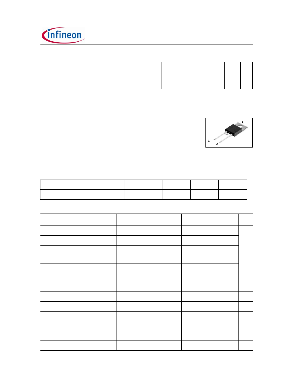
PG-TO220-2-2
thinQ! 2G Diode specially designed for fast switching applications like:
• CCM PFC
• Motor Drives
Type Package Marking Pin 1 Pin 2
I
=5 A, Tj=25 °C
F
IDT05S60C PG-TO220-2-2 D05S60C C A
600 V
12 nC
5 A
Maximum ratings, at T
Parameter Symbol Conditions Unit
Continuous forward current
RMS forward current
Surge non-repetitive forward current,
sine halfwave
Repetitive peak forward current
Non-repetitive peak forward current
i ²t value
Repetitive peak reverse voltage
Diode ruggedness dv/dt dv /dt
Power dissipation
Operating and storage temperature
=25 °C, unless otherwise specified
j
I
F
I
F,RMS
I
F,SM
I
F,RM
I
F,max
2
∫i
V
P
T
RRM
tot
, T
j
TC<140 °C
f =50 Hz 7.5
TC=25 °C, tp=10 ms
Tj=150 °C,
T
=100 °C, D =0.1
C
TC=25 °C, tp=10 µs
dt
C
= 0…480V
V
R
=25 °C, tp=10 ms
T
TC=25 °C
stg
Value
5A
42
21
180
9
2
A
s
600 V
50 V/ns
55 W
-55 ... 175 °C
Mountig torque M3 and M3.5 screws 60 Ncm
Rev. 2.0 page 1 2006-03-14

IDT05S60C
Parameter Symbol Conditions Unit
Values
min. typ. max.
Thermal characteristics
Thermal resistance, junction - case
Thermal resistance,
junction - ambient
Soldering temperature,
wavesoldering only allowed at leads
Electrical characteristics, at T
=25 °C, unless otherwise specified
j
R
thJC
R
thJA
T
sold
leaded - - 62
1.6mm ( 0.063in.) from
case for 10s
- - 2.7 K/W
- - 260 °C
Static characteristics
DC blocking voltage
Diode forward voltage
V
DC
V
F
IR=0.07 mA
IF=5 A, Tj=25 °C
I
=5 A, Tj=150 °C
F
600 - - V
- 1.5 1.7
- 1.7 2.1
Reverse current
I
R
VR=600 V, Tj=25 °C
V
=600 V, Tj=150 °C
R
- 0.6 70 µA
- 2.5 700
AC characteristics
=400 V, IF≤I
V
Total capacitive charge
Switching time
3)
Q
c
t
c
Total capacitance C
1)
J-STD20 and JESD22
2)
All devices tested under avalanche conditions, for a time periode of 5ms, at 5mA.
3)
tc is the time constant for the capacitive displacement current waveform (independent from Tj, I
di/dt), different from t
, which is dependent on Tj, I
rr
R
di
/dt =200 A/µs,
F
T
=150 °C
j
=1 V, f =1 MHz
V
R
V
=300 V, f =1 MHz
R
V
=600 V, f =1 MHz
R
, di/dt. No reverse recovery time constant trr due to
LOAD
F,max
,
-12-nC
- - <10 ns
- 240 - pF
-30-
-30-
absence of minority carrier injection.
4)
Only capacitive charge occuring, guaranteed by design.
LOAD
and
Rev. 2.0 page 2 2006-03-14
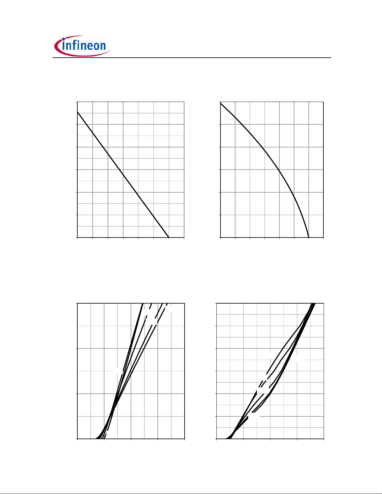
1 Power dissipation 2 Diode forward current
P
=f(TC) IF=f(TC); Tj≤175 °C
tot
parameter: R
thJC(max)
parameter: R
thJC(max)
; V
IDT05S60C
F(max)
60
50
40
[W]
30
tot
P
20
10
0
25 50 75 100 125 150 175 200
TC [°C]
15
12.5
10
7.5
[A]
F
I
5
2.5
0
25 50 75 100 125 150 175 200
TC [°C]
3 Typ. forward characteristic 4 Typ. forward characteristic in surge current
I
=f(VF); tp=400 µs
F
parameter: T
j
mode
IF=f(VF); tp=400 µs; parameter: T
j
15
100 °C
150 °C
10
[A]
F
I
5
0
01234
25 °C
-55 °C
175 °C
VF [V]
60
50
40
-55 °C
30
[A]
F
I
20
10
0
02468
25 °C
100 °C
150 °C
175 °C
VF [V]
Rev. 2.0 page 3 2006-03-14

IDT05S60C
5 Typ. forward power dissipation vs. 6 Typ. reverse current vs. reverse voltage
=f(VR)
average forward current
P
=f(IF), TC=100 °C, parameter: D =tp/T parameter: T
F,AV
30
I
R
j
2
10
25
0.1
0.5
1
1
10
20
[µA]
R
I
10
10
10
10
0
-1
25ºC
-2
-3
-55ºC
175ºC
150ºC
100ºC
100 200 300 400 500 600
VR [V]
0.2
[W]
15
F(AV)
P
10
5
0
024681012
I
[A]
F(AV)
7 Transient thermal impedance 8 Typ. capacitance vs. reverse voltage
Z
=f(tp) C =f(VR); TC=25 °C, f =1 MHz
thJC
parameter: D =t
1
10
/T
p
300
250
0.5
10
[K/W]
thJC
Z
10
10
0
-1
-2
10
0.2
0.1
0.05
0.02
0.01
single pulse
-5
10
10
-3
-4
10
-2
10
-1
10
0
tp [s]
200
150
C [pF]
100
50
0
10
-1
10
0
10
1
10
2
10
3
VR [V]
Rev. 2.0 page 4 2006-03-14

IDT05S60C
9 Typ. C stored energy 10 Typ. capacitance charge vs. current slope
E
=f(VR)
C
=f(diF/dt )4); Tj=150 °C; IF≤I
Q
C
F,max
7
6
5
4
[µC]
c
E
3
2
1
0
0 100 200 300 400 500 600
VR [V]
14
12
10
8
[nC]
c
Q
6
4
2
0
100 400 700 1000
diF/dt [A/µs]
Rev. 2.0 page 5 2006-03-14

PG-TO220-2-2: Outline
IDT05S60C
Dimensions in mm/inches
Rev. 2.0 page 6 2006-03-14

IDT05S60C
Published by
Infineon Technologies AG
81726 München, Germany
© Infineon Technologies AG 2006.
All Rights Reserved.
Attention please!
The information herein is given to describe certain components and shall not be considered as
warranted characteristics.
Terms of delivery and rights to technical change reserved.
We hereby disclaim any and all warranties, including but not limited to warranties of non-infringement,
regarding circuits, descriptions and charts stated herein.
Infineon Technologies is an approved CECC manufacturer.
Information
For further information on technology, delivery terms and conditions and prices, please contact your
nearest Infineon Technologies office in Germany or our Infineon Technologies representatives worldwide
(see address list).
Warnings
Due to technical requirements, components may contain dangerous substances.
For information on the types in question, please contact your nearest Infineon Technologies office.
Infineon Technologies' components may only be used in life-support devices or systems with the
expressed written approval of Infineon Technologies if a failure of such components can reasonably
be expected to cause the failure of that life-support device or system, or to affect the safety or
effectiveness of that device or system. Life support devices or systems are intended to be implanted
in the human body, or to support and/or maintain and sustain and/or protect human life. If they fail,
it is reasonable to assume that the health of the user or other persons may be endangered.
Rev. 2.0 page 7 2006-03-14
 Loading...