

INFINEON IDH05G65C5 Datasheet

SiC
Silicon Carbide Diode
5th Generation thinQ!
650V SiC Schottky Diode
TM
IDH05G65C5
Final Datasheet
Rev. 2.2, 2012-12-10
Power Management & Multimarket
IDH05G65C55th Generation thinQ!™ SiC Schottky Diode
1 Description
ThinQ!™ Generation 5 represents Infineon leading edge technology for the SiC
Schottky Barrier diodes. The Infineon proprietary diffusion soldering process, already
introduced with G3 is now combined with a new, more compact design and thin-wafer
technology. The result is a new family of products showing improved efficiency over
all load conditions, resulting from both the improved thermal characteristics and a
lower figure of merit (Qc x Vf).
The new thinQ!™ Generation 5 has been designed to complement our 650V
CoolMOS™ families: this ensures meeting the most stringent application
requirements in this voltage range.
Features
Revolutionary semiconductor material - Silicon Carbide
Benchmark switching behavior
No reverse recovery/ No forward recovery
Temperature independent switching behavior
High surge current capability
Pb-free lead plating; RoHS compliant
Qualified according to JEDEC
Breakdown voltage tested at 11 mA
Optimized for high temperature operation
1)
for target applications
2)
Benefits
System efficiency improvement over Si diodes
System cost / size savings due to reduced cooling requirements
Enabling higher frequency / increased power density solutions
Higher system reliability due to lower operating temperatures
Reduced EMI
Applications
Switch mode power supply
Power factor correction
Solar inverter
Uninterruptible power supply
Table 1 Key Performance Parameters
Parameter Value Unit
VDC
QC; VR=400V 8 nC
EC; VR=400V 1.8 µJ
IF @ TC < 145°C
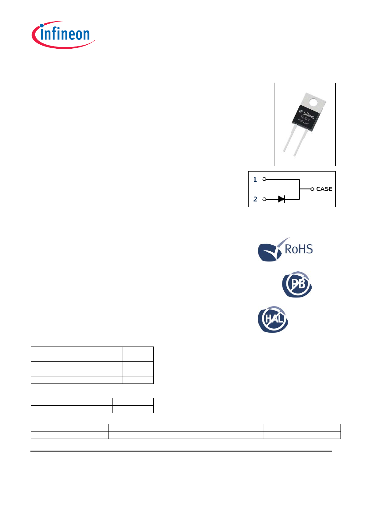
Table 2 Pin Definition
Pin 1 Pin 2 Pin 3
C A n.a.
Type / ordering Code Package Marking Related links
IDH05G65C5 PG-TO220-2 D0565C5 www.infineon.com/sic
650 V
5 A
1
2
1) 1 J-STD20 and JESD22
2) All devices tested under avalanche conditions for a time periode of 10ms
Final Data Sheet 2 Rev. 2.2, 2012-12-10

5
th
Generation thinQ!TM SiC Schottky Diode
IDH05G65C5
Table of contents
Table of Contents
1 Description .......................................................................................................................................... 2
2 Maximum ratings ................................................................................................................................ 4
3 Thermal characteristics ..................................................................................................................... 4
4 Electrical characteristics ................................................................................................................... 5
5 Electrical characteristics diagrams .................................................................................................. 6
6 Simplified Forward Characteristics Model ...................................................................................... 8
7 Package outlines ................................................................................................................................ 9
8 Revision History ............................................................................................................................... 10
Final Data Sheet 3 Rev. 2.2, 2012-12-10
5
th
Generation thinQ!TM SiC Schottky Diode
IDH05G65C5
Maximum ratings
2 Maximum ratings
Table 3 Maximum ratings
Parameter Symbol Values Unit Note/Test Condition
Min. Typ. Max.
Continuous forward current IF – –
Surge non-repetitive forward current,
sine halfwave
Non-repetitive peak forward current I
i²t value
I
– –
F,SM
– –
– –
F,max
∫ i²dt
– –
– –
Repetitive peak reverse voltage V
Diode dv/dt ruggedness
Power dissipation P
Operating and storage temperature Tj;T
Mounting torque
– –
RRM
dv/dt
– –
tot
-55 –
stg
– –
– –
5
46
41
251
10.4
8.4
650
100
55
175
60
TC < 145°C, D=1
A
TC = 25°C, tp=10 ms
TC = 150°C, tp=10 ms
TC = 25°C, tp=10 µs
A²s TC = 25°C, tp=10 ms
TC = 150°C, tp=10 ms
V Tj = 25°C
V/ns VR=0..480 V
W TC = 25°C
°C
Ncm M2.5 screws
3 Thermal characteristics
Table 4 Thermal characteristics TO-220-2
Parameter Symbol Values Unit Note/Test Condition
Min. Typ. Max.
Thermal resistance, junction-case R
Thermal resistance, junctionambient
Soldering temperature,
wavesoldering only allowed at leads
–
thJC
R
thJA
T
sold
– –
– –
1.7 2.7
K/W
62
260
°C 1.6mm (0.063 in.) from
leaded
case for 10 s
Final Data Sheet 4 Rev. 2.2, 2012-12-10
 Loading...