

INFINEON IDD03SG60C Datasheet
IDD03SG60C
3
rd
Generation thinQ!TM SiC Schottky Diode
Features
• Revolutionary semiconductor material - Silicon Carbide
• Switching behavior benchmark
• No reverse recovery / No forward recovery
• Temperature independent switching behavior
• High surge current capability
• Pb-free lead plating; RoHS compliant
• Qualified according to JEDEC
1)
for target applications
thinQ! 3G Diode designed for fast switching applications like:
Maximum ratings
Parameter Symbol Conditions Unit
Continuous forward current
I
F
TC<130 °C
3 A
I
F,SM
TC=25 °C, tp=10 ms
11.5
TC=150 °C, tp=10 ms
9.7
Non-repetitive peak forward current
I
F,max
TC=25 °C, tp=10 µs
100
∫i2dt
TC=25 °C, tp=10 ms
0.61
A2s
TC=150 °C, tp=10 ms
0.44
Repetitive peak reverse voltage
V
RRM
Tj=25 °C
600 V
Diode dv/dt ruggedness
dv/dt
V
R
= 0….480 V
50 V/ns
Power dissipation
P
tot
TC=25 °C
38 W
Operating and storage temperature
Tj, T
stg
-55 ... 175 °C
Soldering temperature, reflow
soldering (max)
T
sold
reflow MSL1 260
• Breakdown voltage tested at 20mA
2)
• Optimized for high temperature operation
• Lowest Figure of Merit Q
C/IF
i²t value
Value
Surge non-repetitive forward current,
sine halfwave
• SMPS e.g.; CCM PFC
• Motor Drives; Solar Applications; UPS
V
DC
600
V
Q
C
3.2
nC
IF; TC< 130 °C
3
A
Product Summary
Type
Package
Marking
Pin 1
Pin 2
Pin 3
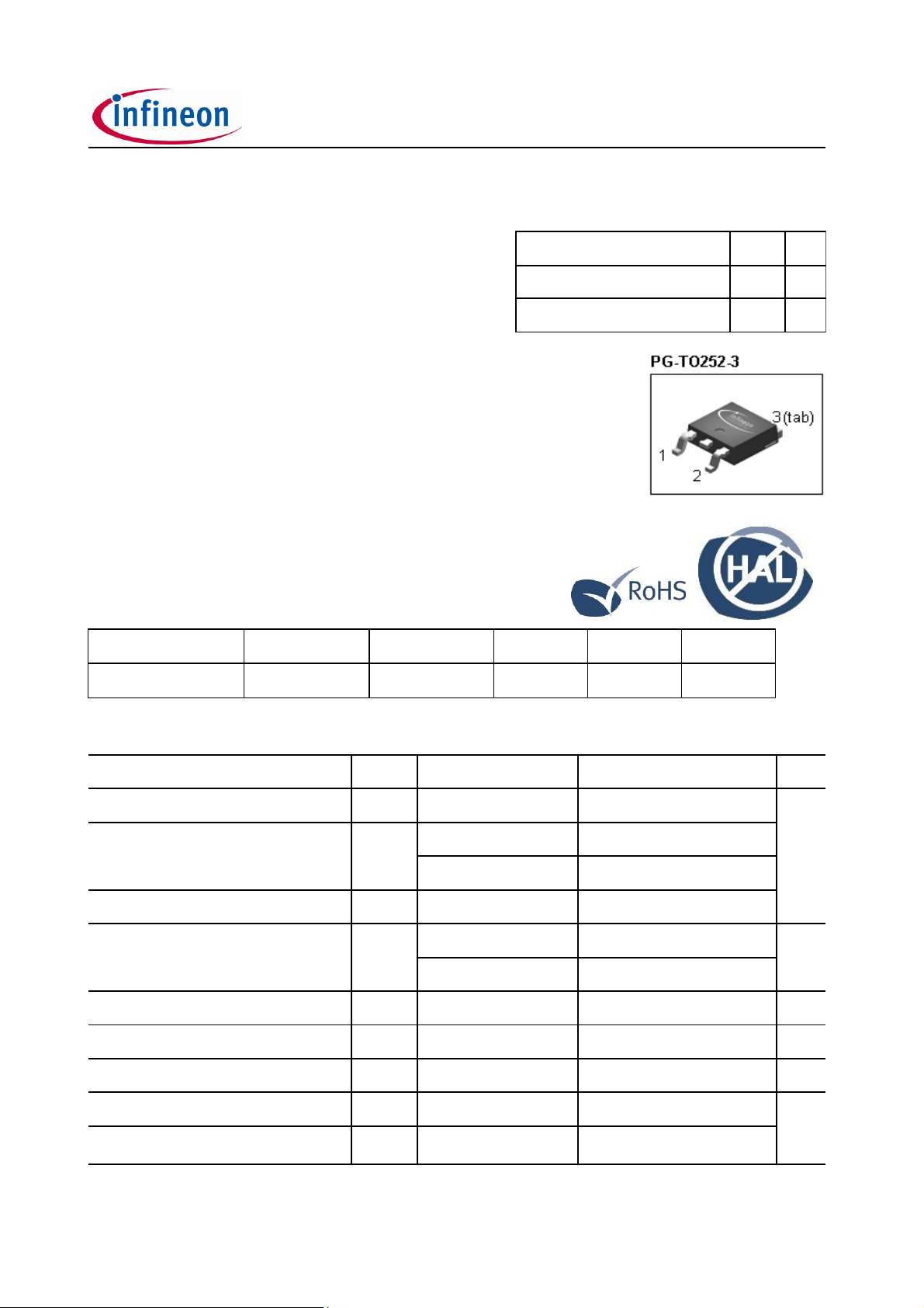
IDD03SG60C
PG-TO252-3
D03G60C
n.c.
A
C
Rev. 2.4 page 1 2013-02-11
IDD03SG60C
Parameter Symbol Conditions Unit
min. typ. max.
Thermal characteristics
Thermal resistance, junction - case
R
thJC
- - 3.9 K/W
R
thJA
SMD version, device
on PCB, minimal
footprint
- - 75
SMD version, device
on PCB, 6 cm2 cooling
area
5)
- 50 -
Electrical characteristics, at Tj=25 °C, unless otherwise specified
Static characteristics
DC blocking voltage
V
DC
IR=0.05 mA, Tj=25 °C
600 - - V
Diode forward voltage
V
F
IF=3 A, Tj=25 °C
- 2.1 2.3
IF=3 A, Tj=150 °C
- 2.8 -
Reverse current
I
R
VR=600 V, Tj=25 °C
- 0.23 15 µA
VR=600 V, Tj=150 °C
- 1 150
AC characteristics
Total capacitive charge
Q
c
- 3.2 - nC
Switching time
3)
t
c
- - <10 ns
Total capacitance
C
VR=1 V, f=1 MHz
- 60 - pF
VR=300 V, f=1 MHz
- 8 -
VR=600 V, f=1 MHz
- 8 -
1)
J-STD20 and JESD22
2)
All devices tested under avalanche conditions, for a time periode of 10ms, at 20mA.
3)
tc is the time constant for the capacitive displacement current waveform (independent from Tj, I
LOAD
and
di/dt), different from trr which is dependent on Tj, I
LOAD
and di/dt. No reverse recovery time constant trr due
to absence of minority carrier injection.
Values
VR=400 V,IF≤I
F,max
,
diF/dt=200 A/µs,
Tj=150 °C
Thermal resistance, junction ambient
6)
Only capacitive charge occuring, guaranteed by design.
4)
Under worst case Zth conditions.
5)
Device on 40mm*40mm*1.5 epoxy PCB FR4 with 6cm² (one layer, 70µm thick) copper area for drain
connection. PCB is vertical without blown air
Rev. 2.4 page 2 2013-02-11
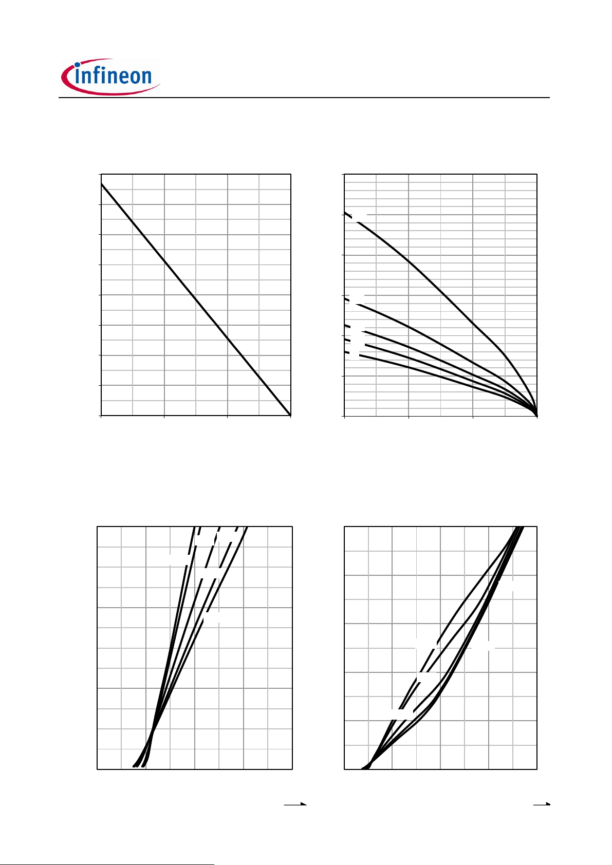
IDD03SG60C
1 Power dissipation 2 Diode forward current
P
tot
=f(TC); parameter: R
thJC(max)
IF=f(TC)4); Tj≤175 °C; parameter: D = tp/T
3 Typ. forward characteristic 4 Typ. forward characteristic in surge current
mode
IF=f(VF); tp=400 µs; parameter:T
j
IF=f(VF); tp=400 µs; parameter: T
j
0
5
10
15
20
25
30
35
40
25 75 125 175
P
tot
[W]
TC [°C]
-55ºC
25ºC
100ºC
150ºC
175ºC
0
1
2
3
0 1 2 3 4
I
F
[A]
VF[V]
-55ºC
25ºC
100ºC
150ºC
175ºC
0
3
6
9
12
15
0 2 4 6 8
I
F
[A]
VF[V]
1
0.7
0.5
0.3
0.1
0
5
10
15
20
25
30
25 75 125 175
I
F
[A]
TC [°C]
Rev. 2.4 page 3 2013-02-11
 Loading...