

Page 1

Industrial & Multimarket
Application Note
Version 2.0, 2011-04-14
ICL8001G / ICLS8082G
Design Guidelines
Phase-Cut-Dimmable Single-Stage LED Driver with PFC
using Quasi-Resonant Primary Power Control
Version 2.0
LED Driver ICs
Page 2

Edition 2011-04-14
Published by
Infineon Technologies AG
81726 Munich, Germany
© 2011 Infineon Technologies AG
All Rights Reserved.
Legal Disclaimer
The information given in this document shall in no event be regarded as a guarantee of conditions or
characteristics. With respect to any examples or hints given herein, any typical values stated herein and/or any
information regarding the application ofthedevice,Infineon Technologies hereby disclaims anyand allwarranties
and liabilities of any kind, including without limitation, warranties of non-infringement of intellectual property rights
of any third party.
Information
For further information on technology, delivery terms and conditions and prices, please contact the nearest
Infineon Technologies Office (www.infineon.com).
Warnings
Due to technical requirements, components may contain dangerous substances. For information on the types in
question, please contact the nearest Infineon Technologies Office.
Infineon Technologies components may be used in life-support devices or systems only with the express written
approval ofInfineon Technologies, ifafailureofsuchcomponentscanreasonablybeexpectedtocausethefailure
of that life-support device or system or to affect the safety or effectiveness of that device or system. Life support
devices or systems are intended to be implanted in the human body or to support and/or maintain and sustain
and/or protect human life. If they fail, it is reasonable to assume that the health of the user or other persons may
be endangered.
Page 3

ICL8001G / ICLS8082G
Design Guidelines
Application Note 3 Version 2.0, 2011-04-14
ICL8001G / ICLS8082G Design Guidelines
werner.ludorf@infineon.com
Revision History: 2011-04-14, Version 2.0
Previous Revision:
Page Subjects (major changes since last revision)
First edition
Page 4

ICL8001G / ICLS8082G
Design Guidelines
Table of Contents
Application Note 4 Version 2.0, 2011-04-14
Table of Contents . . . . . . . . . . . . . . . . . . . . . . . . . . . . . . . . . . . . . . . . . . . . . . . . . . . . . . . . . . . . . . . . 4
1 Introduction . . . . . . . . . . . . . . . . . . . . . . . . . . . . . . . . . . . . . . . . . . . . . . . . . . . . . . . . . . . . . . . . . . . . . 5
2 Pin Configuration and Functionality . . . . . . . . . . . . . . . . . . . . . . . . . . . . . . . . . . . . . . . . . . . . . . . . . 6
2.1 Pin Configuration with PG-DSO-8 . . . . . . . . . . . . . . . . . . . . . . . . . . . . . . . . . . . . . . . . . . . . . . . . . . . . 6
2.2 Package PG-DSO-8 . . . . . . . . . . . . . . . . . . . . . . . . . . . . . . . . . . . . . . . . . . . . . . . . . . . . . . . . . . . . . . . 7
2.3 Pin Functionality . . . . . . . . . . . . . . . . . . . . . . . . . . . . . . . . . . . . . . . . . . . . . . . . . . . . . . . . . . . . . . . . . . 7
3 Control Principle . . . . . . . . . . . . . . . . . . . . . . . . . . . . . . . . . . . . . . . . . . . . . . . . . . . . . . . . . . . . . . . . . 8
4 Design Parameters . . . . . . . . . . . . . . . . . . . . . . . . . . . . . . . . . . . . . . . . . . . . . . . . . . . . . . . . . . . . . . . 9
4.1 Transformer Parameters . . . . . . . . . . . . . . . . . . . . . . . . . . . . . . . . . . . . . . . . . . . . . . . . . . . . . . . . . . . . 9
4.2 Power Switch . . . . . . . . . . . . . . . . . . . . . . . . . . . . . . . . . . . . . . . . . . . . . . . . . . . . . . . . . . . . . . . . . . . 10
4.3 Primary Peak Current Control . . . . . . . . . . . . . . . . . . . . . . . . . . . . . . . . . . . . . . . . . . . . . . . . . . . . . . . 11
4.4 Foldback Correction . . . . . . . . . . . . . . . . . . . . . . . . . . . . . . . . . . . . . . . . . . . . . . . . . . . . . . . . . . . . . . 12
4.5 Switch-on Determination for Quasi-resonant Operation . . . . . . . . . . . . . . . . . . . . . . . . . . . . . . . . . . . 13
4.6 Power Factor Correction . . . . . . . . . . . . . . . . . . . . . . . . . . . . . . . . . . . . . . . . . . . . . . . . . . . . . . . . . . . 14
4.7 VCC for Dimming . . . . . . . . . . . . . . . . . . . . . . . . . . . . . . . . . . . . . . . . . . . . . . . . . . . . . . . . . . . . . . . . 14
5 Design Optimizations . . . . . . . . . . . . . . . . . . . . . . . . . . . . . . . . . . . . . . . . . . . . . . . . . . . . . . . . . . . . 15
5.1 Dimming . . . . . . . . . . . . . . . . . . . . . . . . . . . . . . . . . . . . . . . . . . . . . . . . . . . . . . . . . . . . . . . . . . . . . . . 15
5.1.1 Dimming Principle . . . . . . . . . . . . . . . . . . . . . . . . . . . . . . . . . . . . . . . . . . . . . . . . . . . . . . . . . . . . . . 15
5.1.2 Dimmer Compatibility . . . . . . . . . . . . . . . . . . . . . . . . . . . . . . . . . . . . . . . . . . . . . . . . . . . . . . . . . . . . 17
5.1.3 Dimmer List . . . . . . . . . . . . . . . . . . . . . . . . . . . . . . . . . . . . . . . . . . . . . . . . . . . . . . . . . . . . . . . . . . . 18
5.1.4 Dimmer Selection . . . . . . . . . . . . . . . . . . . . . . . . . . . . . . . . . . . . . . . . . . . . . . . . . . . . . . . . . . . . . . 19
5.2 Power Stabilization for Line Voltage Variations . . . . . . . . . . . . . . . . . . . . . . . . . . . . . . . . . . . . . . . . . 19
5.2.1 Stabilization using IC Foldback Correction . . . . . . . . . . . . . . . . . . . . . . . . . . . . . . . . . . . . . . . . . . . 19
5.2.2 Discrete Power Stabilization Circuit for ICL8001G . . . . . . . . . . . . . . . . . . . . . . . . . . . . . . . . . . . . . 20
5.3 Optimized Power Factor Correction Performance . . . . . . . . . . . . . . . . . . . . . . . . . . . . . . . . . . . . . . . 22
6 Protection Functions . . . . . . . . . . . . . . . . . . . . . . . . . . . . . . . . . . . . . . . . . . . . . . . . . . . . . . . . . . . . 23
6.1 Output OVP . . . . . . . . . . . . . . . . . . . . . . . . . . . . . . . . . . . . . . . . . . . . . . . . . . . . . . . . . . . . . . . . . . . . 23
6.2 Output Short Circuit Protection . . . . . . . . . . . . . . . . . . . . . . . . . . . . . . . . . . . . . . . . . . . . . . . . . . . . . . 23
6.3 Input Overvoltage Protection (OVP) . . . . . . . . . . . . . . . . . . . . . . . . . . . . . . . . . . . . . . . . . . . . . . . . . . 23
7 Explicit Questions and Answers . . . . . . . . . . . . . . . . . . . . . . . . . . . . . . . . . . . . . . . . . . . . . . . . . . . 24
7.1 Application . . . . . . . . . . . . . . . . . . . . . . . . . . . . . . . . . . . . . . . . . . . . . . . . . . . . . . . . . . . . . . . . . . . . . 24
7.2 Control Principle . . . . . . . . . . . . . . . . . . . . . . . . . . . . . . . . . . . . . . . . . . . . . . . . . . . . . . . . . . . . . . . . . 24
8 References . . . . . . . . . . . . . . . . . . . . . . . . . . . . . . . . . . . . . . . . . . . . . . . . . . . . . . . . . . . . . . . . . . . . 25
Table of Contents
Page 5

ICL8001G / ICLS8082G
Design Guidelines
Introduction
Application Note 5 Version 2.0, 2011-04-14
1 Introduction
Objective
The objective of this application note is to describe how adimmable, highly efficient single-stage LED driver based
on the ICL8001G / ICLS8082G primary control developed by Infineon Technologies AG can be designed and how
different design targets can be considered. For this purpose, quantitative design tools for dimensioning of the
flyback transformer for QR (quasi-resonant) operation and further discrete components relevant to the power
factor correction (PFC) and dimming control functions are provided. The design process refers to a concrete
application example of a phase cut dimmable LED driver. Explicit questions and answers are treated in conclusion.
Features of ICL8001G / ICLS8082G control
• High, stable efficiency over a wide operating range
• Optimized for trailing and leading-edge dimmers
• Precise PWM for primary PFC and dimming control
• HV power cell for VCC precharging with a constant current
• Built-in digital soft start
• Foldback correction and cycle-by-cycle peak current limitation
• VCC over/undervoltage lockout
• Auto restart mode for short circuit protection
• Adjustable latch-off mode for output overvoltage protection (OVP)
Description
The ICL8001G / ICLS8082G employs a quasi-resonant (QR) operation mode and, due to the availability of
outstanding PFC performance, is optimized for off-line LED lighting applications such as dimmable LED bulbs for
incandescent lamp replacement, LED downlights and LED tubes in a power range from typically 5 W to 50 W.
Precise PWM generation enables primary control for phase cut dimming and potential for high power factors of
PF > 99 %. Depending on the power class, significantly improved driver efficiency of up to 91 % is feasible. The
product has a wide operation range of IC voltage supply and low power consumption. Multiple safety functions
ensure full system protection in failure situations. With its full feature set and simple application, the ICL8001G /
ICLS8082G represents an outstanding choice for QR flyback designs combining feature set and performance at
a minimum BOM cost.
Page 6
ICL8001G / ICLS8082G
Design Guidelines
Pin Configuration and Functionality
Application Note 6 Version 2.0, 2011-04-14
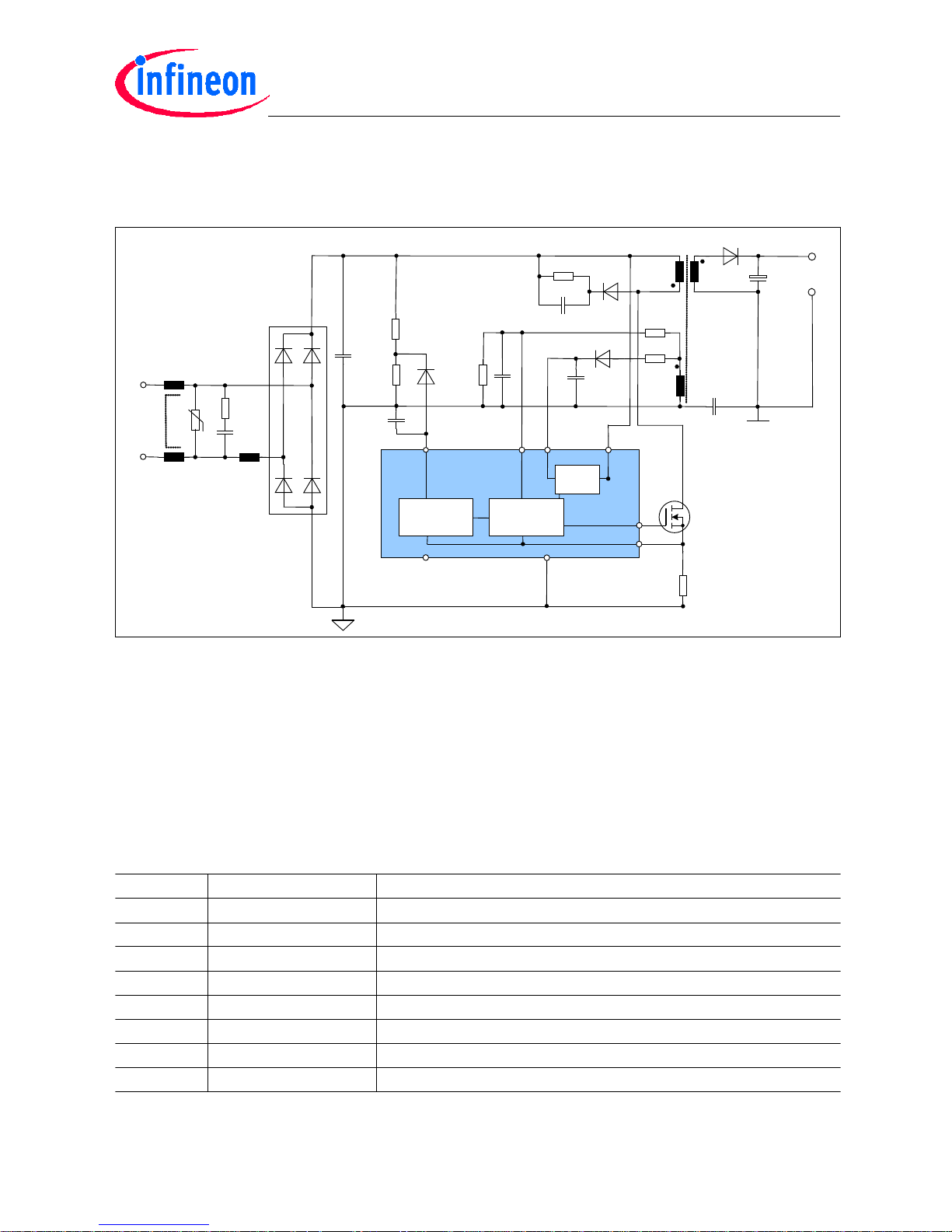
Application circuit
Figure 1 below shows the application circuit for the ICL8001G.
Figure 1 ICL8001G application circuit
2 Pin Configuration and Functionality
2.1 Pin Configuration with PG-DSO-8
Table 1 Pin Configuration for PG-DSO-8
Pin Symbol Function
1 ZCV Zero Crossing
2 VR Voltage Sense
3 CS Current Sense
4 GD Gate Drive Output
5 HV High Voltage Input
6 n.c. Not connected
7 VCC Controller Supply Voltage
8 GND Controller Ground
Cx
Cin
Rn
Cn
Dn
Cvcc
Dvcc
Rs
Do Co
L1
Rvcc
VCC
GND
T1
npnans
Rzc1
Rzc2
ZCV
ICL8001G
Vo
Vac
BR
Czc
VR
PWM-Control
Protection
GateDriver
Start-Up
Cell
Vm( Vs )
Cc
CS
Ro
Ru
NC
HV
GD
DR
Q1
CR
Rv
L2
Rc
U1
Vin
Page 7

ICL8001G / ICLS8082G
Design Guidelines
Pin Configuration and Functionality
Application Note 7 Version 2.0, 2011-04-14
2.2 Package PG-DSO-8
Figure 2 Pin Configuration of PG-DSO-8 (top view)
2.3 Pin Functionality
ZCV (Zero Crossing)
The voltage from the auxiliary winding after a time delay circuit is applied at this pin. Internally, the pin is connected
to the zero-crossing detector for switch-on determination. Additionally, the output overvoltage detection is realized
by comparing the voltage Vzc with an internal preset threshold.
VR (Voltage Sense)
The rectified input mains voltage is sensed at this pin. The signal is used to set the peak current ofthepeak-current
control and therefore enable the PFC and phase-cut dimming functionality.
CS (Current Sense)
This pin is connected to the shunt resistor for the primary current sensing, externally, and to the PWM signal
generator for switch-off determination (together with the feedback voltage), internally. Moreover, short-winding
protection is realized by monitoring the voltage Vcs during on-time of the main power switch.
GD (Gate Drive Output)
This output signal drives the external main power switch, which is a power MOSFET in most cases.
HV (High Voltage)
The HV pin is connected to the bus voltage, externally, and to the power cell, internally. The current through this
pin precharges the VCC capacitor with a constant current once the supply bus voltage is applied.
VCC (Power supply)
The VCC pin is the positive supply of the IC. The operating range is between V
VCCoff
and V
VCCOVP
.
GND (Ground)
This is the common ground of the controller.
ZCV
VR
CS
GD
GND
VCC
NC
HV
1
2
3
4 5
6
7
8
Page 8
ICL8001G / ICLS8082G
Design Guidelines
Control Principle
Application Note 8 Version 2.0, 2011-04-14
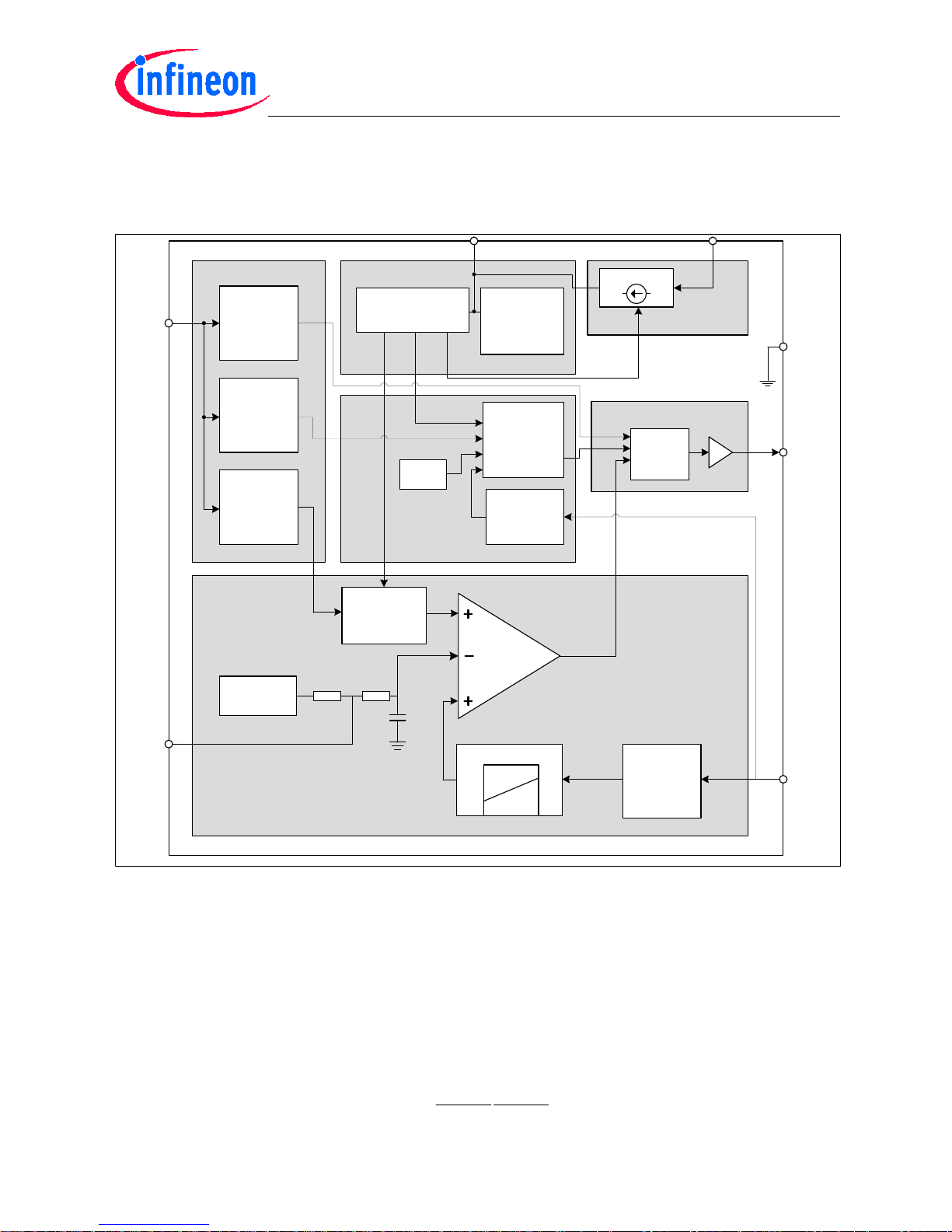
3 Control Principle
Figure 3 Block diagram of the ICL8001G
An inspection of the ICL8001G block diagram shows that the voltage measured at the shunt resistor Rs (see also
the application circuit in Figure 1), which varies according to the instant transformer primary current Ip(t),
determines the gain voltage VG as
(1)
With the PWM OPgain G
PWM
and the offset voltage ram V
PWM
VG is compared to the voltage VR, which is derived
from the input voltage divider (Ro, Ru). This means that the peak current through the power switch Q1 and the
primary inductance L varies according to the instant input voltage Vin(t) as expressed by
(2)
Depl. CoolMOS
Startup Cell
Power ManagmentZero Crossing
PWM Control
Gate Drive
Protection
HV
GND
GD
Gate
Control
Voltage
Reference
& Biasing
Over / Under-
Voltage Lockout
OTP
Restart /
Latchup
Control
VCC
CS
Leading
Edge
Blanking
VR
ZCV
Zero
Current
Detection
Over
Voltage
Protection
PM / PFC
Control
Foldback
Correction
Short
Winding
Detection
VG ( Vs )
PWM
Comparator
V
REF
V
FB
25k
2pF
PWMsPWM
VRtIpGtIpVG )())((
RsG
tVin
RuRo
Ru
tIp
PWM
)(
)(
Page 9

ICL8001G / ICLS8082G
Design Guidelines
Design Parameters
Application Note 9 Version 2.0, 2011-04-14
It can be seen in the non-dimming case that asinusoidal waveform of the primary peak current is dominant, which
defines the almost sinusoidal shape of the input current Iin(t). Beside the PFC function Equation (2) above shows
that during phase cut dimming the input current will follow the phase cut-modified input voltage, which assures the
dependence of the driver output power on the RMS input voltage V
rms
according to the law described by
Equation (24) on page 15.
4 Design Parameters
This chapter presents the essential design process and illustrates it in parallel with concrete values which are
considered for a sample design with the main target magnitudes VLED = 27 V, ILED = 360 mA, PF = 98 %,
η = 90 %, f < fmax = 100 kHz for the input parameters Vin = 230 V, fin = 50 Hz and Pin = VLED ILED / (η PF). The
values chosen for the 10 W/230 V LED driver demo board are close to the following calculation results.
4.1 Transformer Parameters
For QR operation, a sufficiently large reflected voltage from the secondary to the primary side present during the
flyback time tf has to be provided. After discharge of the transformer by means of the secondary winding current
the energy coupled to the reflected voltage is needed to reduce the input voltage at switch-on instantly in the VDS
valley to Vdsmin = Vin - Vr. With the selection of Vdsmin = 0 a value Vr = Vinp, where
(3)
is received according to
(4)
The ratio q = Vr / Vinp with q ≤ 1 determines the maximum input voltage Vinp to be processed with zero-voltage
switching. The winding ratio rn= np / ns is then calculated as rn= 12.
(5)
The driver operation frequency f varies over the line voltage phase and reaches its maximum values in the line
voltage phase close to the voltage peak Vinp. Consideration of a QR mode condition defines the primary
inductance L = 6.1 mH (6.3 mH chosen) based on
(6)
With the selection f = fmax, the equation for the minimum on-time
(7)
yields ton = 5.0 µs and so the minimum duty cycle becomes Dmin = 0.5 as
(8)
VinVinp 2
minVdsVinpVr
Vdo
VLED
V
r
r
n
2
2
1
2
Vr
Vinp
fPin
Vin
L
Vinf
PinL
ton12
Vin
fPinLD2
min
Page 10

ICL8001G / ICLS8082G
Design Guidelines
Design Parameters
Application Note 10 Version 2.0, 2011-04-14
Now the maximum primary peak current arising in the line phase with Vin = Vinp can be fixed as I
pmaxp
= 0.27 A
according to
(9)
Assuming a saturation inductance of Bm = 0.4 T and Ae = 20.1 mm2a minimum number of primary turns of
np ≈ 200 (np = 190 chosen) would be obtained.
(10)
The maximum magnetic permeance ALmax = 170 nH is obtained using
(11)
which determines the air gap using the k-factors in
(12)
For the often relevant E16-core, the k-factors are k1 = 42.2 and k2 = –0.701 resulting in s ≈ 0.15 mm. The
secondary number of turns is then given by
(13)
By choosing ns = 14 and the centered IC supply voltage Vccc = ( Vccmax + Vccmin )/ 2 = 19 the auxiliary winding
number will be na = 10 according to
(14)
4.2 Power Switch
The maximum voltage V
DSmax
along the drain-source path of the MOSFET arises during the line phase with Vin
= Vinp at the instant just subsequent to switching off the primary current. In this phase the high-frequency
oscillation amplitude
(15)
adds to the superposition given by the input voltage and reflected voltage to
(16)
The V
DSmax
value can be limited by either reducing the QR effect (with q) at the cost of driver efficiency or by
damping the oscillation by means of a snubber circuit. These limiting approaches can be compared in terms of
fL
Pin
I
pp2max
BmAe
IL
np
ppmax
min
2
max
np
L
AL
2
1
9
1
10max
k
k
AL
s
n
r
np
ns
Vdo
VLED
Vcc
nsna
max
Cds
Ls
IVosc
pp max
oscinpDS
VqVV )1(
max
Page 11

ICL8001G / ICLS8082G
Design Guidelines
Design Parameters
Application Note 11 Version 2.0, 2011-04-14
cost and efficiency reduction with the option of choosing MOSFETs with higher breakdown voltages. For high
efficiency it is recommended to make the adjustment V
DSmax
= 2 Vinp + Vosc < 800 V or 900 V respectively. If
necessary, a transformer design with q < 1 (meaning reduced QR operation effect) should be favored over high
snubber losses.
4.3 Primary Peak Current Control
The peak current charging the primary inductance of the transformer reaches its maximum value at the input
voltage Vinp. By choosing the maximum threshold Vcsmax = 0.75 V for the shunt voltage generated at the instant
of Vinp, the shunt resistance is Rs = 2.7 Ω based on
(17)
The upper resistor, Ro, in the input voltage divider is dimensioned in consideration of losses and PFC. For
efficiency optimization, high ohmic values are preferred. A low ohmic input voltage divider enables a maximum
power factor adjustment.
The resistance of the lower input voltage divider resistor is expressed as
(18)
For the selection Vcsmax ≈ 0.75V and Rs = 2.7 Ω the Ru equation above helps to define (with the specification of
Ro = 560 kΩ) a resistance of Ru = 4.3 kΩ (choose Ru = 3.9 kΩ).
pp
I
Vcs
Rs
max
max
RsIGVinp
IGRsRo
Ru
ppPWM
ppPWM
max
max
Page 12

ICL8001G / ICLS8082G
Design Guidelines
Design Parameters
Application Note 12 Version 2.0, 2011-04-14
4.4 Foldback Correction
When the line input voltage increases, the comparator threshold for switching off the power switch is reached in a
shorter time and the resulting increase in operation frequency would lead to a strong increase in the LED driver
power. To limit the input voltage dependence above a certain limit Vinth, the foldback correction reduces the
threshold Vcsmax(Icz) in accordance with the current detected at the ZCD pin as expressed here:
(19)
The characteristic curve Vcsmax(Izc) implemented in the IC shows the following steps:
Figure 4 Vcsmax(lzc) characteristic curve
For the adjusted setting Vinth = Vinp and selection of the foldback operation point Vcs-max = 0.75 V / Icz = 1 mA,
using the characteristic curve the detection resistance is calculated to be Rzc1 ≈ 15 kΩ according to
(20)
From the characterisitic curve it can be seen that the Vin dependence of Vcsmax is stronger in the range of higher
threshold values. This means that if a strong impact of the foldback correction is desired, the Vcs should reach
rather high values at Vinp. For increased power constancy under input voltage voltage variations, higher values
of R4 and R19 should be chosen.
np
na
Rcz
Vin
VinIcz1)(
np
na
Icz
thVin
Rcz 1
Page 13

ICL8001G / ICLS8082G
Design Guidelines
Design Parameters
Application Note 13 Version 2.0, 2011-04-14
4.5 Switch-on Determination for Quasi-resonant Operation
For ideal quasi-resonant operation the switch-on of the power switch should occur when the transformer current
in the output circuit reaches zero and half of theoscillation period (oscillation 2 inFigure 5) definedby the leakage
inductance and the drain-source capacitance of the power switch has elapsed.
Figure 5 Determination of the switch-on instant
The delay td elapses from the instant of discharging the transformer to when the first VDS valley is reached. For
initial dimensioning of the delay circuit the relationship
(21)
can be used. For the 230 V / 10 W demo board an initial value of td ≈ 1 µs is appropriate. For output overvoltage
protection with final shutdown at Vo > 45 V it turns out to be useful to choose Rzc2 ≈ 2 kΩ. Consequently, the
capacitance of the delay circuit Czc = 580 pF (choose Czc = 470 pF) will be obtained according to
(22)
CdsLtd
2121RzcRzc
RzcRzc
tdCzc
Page 14

ICL8001G / ICLS8082G
Design Guidelines
Design Parameters
Application Note 14 Version 2.0, 2011-04-14
4.6 Power Factor Correction
The PFC function provides a sinusoidal input current waveform. For this, the setpoint at pin VR should be related
strongly to the input voltage waveform Vin(t). The internal reference voltage Vref is connected via the internal
resistor VFB to the pin VR. The voltage waveform VR(t) over the line period can be influenced in such a way that
a more trapezoidal curve is generated and the input current waveform behaves accordingly. An input voltage
divider with Ro ≈ 500 kΩ at Vac = 230 V delivers a high power factor of typically PF > 95 % and dissipates low
power for high driver efficiency. High PF values above 99 % and low total harmonic distortion of typically 10 % are
achievable at decreased power tolerances. If high power factor adjustment has priority, it is also important to select
an elevated threshold for foldback correction Vinth ≈ Vinp.
Figure 6 Power factor correction
4.7 VCC for Dimming
The dimming feature is closely coupled to the PF control as the variation of the setpoint VR(t) determines the
power flow to the QR-operated flyback. This is also true if the input voltage is shaped by means of a phase cut
dimmer, regardless of whether this is a trailing or leading edge wall dimmer. Therefore thevariation of the effective
input voltage determines thepower level supplied to theLED load at the driver output. The low frequency variation
of the input power is smoothened by means of an output capacitor Co storing enough energy to cause no visible
light flickering.
For a stable IC supply voltage at phase cut dimming more severe conditions have to be observed. Extended
temporal gaps with zero input voltage, especially at low dimming levels, are present. Also a certain decrease in
output voltage is present in the continuous dimming state of the LED. The Vcc capacitor Cvcc can be designed
using
(23)
For dimming applications the assumptions of voltage variation ∆VCCdim = 5 V, IVCC = 5 mA and Tgap
≈ 2 x 10 ms for line half-periods with phase cut dimmer malfunction, a Cvcc ≈ 20 µF would be required, while for
non-dimming application the capacitance requirement could be half of that value. For dimmable drivers with Cvcc
= 22 µF a short time of 300 ms to light can be realized due to the charging current provided by the HV start-up cell.
dim
VCC
TgapIVCC
Cvcc
Page 15

ICL8001G / ICLS8082G
Design Guidelines
Design Optimizations
Application Note 15 Version 2.0, 2011-04-14
5 Design Optimizations
5.1 Dimming
5.1.1 Dimming Principle
The LED driver input voltage at phase cut dimming with the switching instant ts will generate an effective voltage
of Vineff(ts). From the applied dimming principle it can be seen that the LED power will depend on Vineff(ts)
according to the proportionality law
(24)
where 1.5 < x < 2.0. Consequently, the light level depends on the RMS input voltage Vrms(ts) provided by the
phase cut dimmer and the dimming range is therefore given by the phase-cut limits of the wall dimmer. For the
example of a trailing edge dimmer, the following diagrams show the time dependence of the modified input voltage
V(t,ts) with the fixed parameter switching instant ts = T/4 and the RMS input voltage Vrms(ts) during a theoretical
full variation of switching instants ts for visualization of the mathematical function Vrms(ts).
Figure 7 Timing dependency on input voltage
Figure 8 Timing dependency on RMS input voltage
x
tsVrmstsVrmsPLED ))(())((
Page 16

ICL8001G / ICLS8082G
Design Guidelines
Design Optimizations
Application Note 16 Version 2.0, 2011-04-14
Phase cut dimming arrangement
Figure 9 Phase cut dimming arrangement
The experimental dependence PLED(Vrms) is illustrated using a 40 Weq LED bulb driver controlled with a trailing
edge phase cut dimmer.
Figure 10 Output power versus input trail edge Vrms
Effective for the application is the dependence of the LED driver power on the switching instant ts / switching angle.
The following experimental diagram obtained with an Ehmann trailing edge dimmer shows the dependence of the
switching instant ts on the driver input power (upper curve) and LED power (lower curve) respectively.
Figure 11 Relationship between switch-off instant ts and power
Phase Cut Dimmer
ICL8001G
LED Driver
LED Array
Vac
+
_
Vac
VLED
+
_
Page 17

ICL8001G / ICLS8082G
Design Guidelines
Design Optimizations
Application Note 17 Version 2.0, 2011-04-14
The lower curve corresponds closely to the lumen flux of the LED array supplied by the driver and illustrates a
continuous increase for the switching angle variation at the wall dimmer.
5.1.2 Dimmer Compatibility
The driver operation with TRIAC dimmers makes it necessary to observe the requirements regarding their holdup currents. In addition, the steep rising voltage slopes can excitate disturbing interactions with the parasitics of
the EMI filter of the driver. To dampen these interactions it is useful to implement a low-pass filter close to the EMI
filter. As placement of the filter in front of the input rectifier would decrease the EMI filter performance it is
recommendable to choose a position parallel to the input voltage divider. In the circuit diagram further below, an
R-C circuit is implemented. Dimensioning of R8 = 220 Ω and C8 = 68 nF (not integrated in the standard demo
board layout) provides stabilization for leading-edge dimmer operation. The non-dimming driver efficiency is
reduced by only typically 1 %.
Figure 12 Extended application circuit for dimming
Especially for applications with low input voltage and resulting higher input currents, shaping of the input current
waveforms has been shown to be effective in achieving dimming stability. For this, an increase in the ratio
R17 / (R17+ R19) and increasein R4 for keeping the LED power constant is suggested. The principal modification
of the modification on the different waveforms is indicated in Figure 13 below.
C1
C11
R1
C12
D5
C15
D6
R4
D21 C25
L1
R2
VCC
GND
T1
npnans
R6
R3
ZCV
ICL8001G
VLED
Vac
BR1
C18
VR
PWM-Control
Protection
GateDriver
Start-Up
Cell
ContinuousMode
DIM Control
PFC
C5
CS
R19
R17
NC
HV
GD
D7
Q1
C17
R5
L2
R7
Vin
C8
R8
5
3
1
2
6
8
Page 18

ICL8001G / ICLS8082G
Design Guidelines
Design Optimizations
Application Note 18 Version 2.0, 2011-04-14
Figure 13 Input current waveforms
For an input supply voltage of 100 V the resistors have been changed accordingly: R19 from 3.9 kΩ to 10 kΩ, R19
from 150 kΩ to 300 kΩ and R4 from 2.2 Ω to 2.7 Ω. The increased dimmer compatibility decreases the power
factor from 99 % to 86 %. This modification can be combined with dimensioning for a stronger effect of the
foldback correction. Designs with an increased VR voltage level will lead to a reduction in driver efficiency.
5.1.3 Dimmer List
Table 2 Input voltage 230 V / 10 W
Manufacturer Type/designation Power limit Dimming range
PDL Leading Edge CAT634LM 450 W 20 – 100 %
Busch Leading Edge 2200 400 W 16 – 100 %
Ehmann Leading Edge T10 300 W 3 – 100 %
Ehmann Trailing Edge T46 315 W 23 – 100 %
HPM Trailing Edge Cat400T 400 W 6 – 100 %
PDL Trailing Edge CAT624TM 450 W 10 – 100 %
Table 3 Input voltage 100 V / 10 W
Manufacturer Type/designation Power limit Dimming range
LEVITON Leading Edge decora RPI06 600 W 11 – 100 %
LEVITON Leading Edge TRIMATRON 6684 600 W 5 – 100 %
LUTRON Leading Edge SKYLARK S-600H-WH 600 W 3 – 100 %
LUTRON Leading Edge SKYLARK S-600P 600 W 4 – 100 %
LUTRON Leading Edge TOGGLER TG-600PH-IV 600 W 9 – 100 %
Page 19

ICL8001G / ICLS8082G
Design Guidelines
Design Optimizations
Application Note 19 Version 2.0, 2011-04-14
5.1.4 Dimmer Selection
With ICL8001G / ICLS8082G control the LED driver can be operated without a wall dimmer as well as using
trailing- and leading-edge dimmers. With the phase-cut dimmers applied above, a satisfying light quality and
variation in the LED lumen flux over the dimming range has been achieved. For both technologies the phase-cut
range should be sufficiently large to provide the dimming range required. The dimming range available with a
particular dimmer for incandescent lamps is directly transferred to the LED driver with ICL8001G / ICLS8082G,
but the lumen output of the LEDs at the minimum dimming position will be higher than with incandescent lamps
as they need a high amount of thermal power to enable the visible light radiation process.Particularly for operation
with 230 V input voltage, leading-edge wall dimmers with a lower rated power range – and hence lower hold-up
current requirements – should be selected in order to prevent the occurrence of repetitive TRIAC ignition.
Operation with lower input voltages, such as 110 V, provides a higher input current, which in principle supports
more stable TRIAC operation.
Touch dimmers with internal IC control, which depends exclusively on a resistive load for sufficient digital IC
supply, should not be selected for LED driver control.
5.2 Power Stabilization for Line Voltage Variations
For stable lumen output and limitation of LED power during mains voltage variations it may be useful to consider
power stabilization for the LED driver design. This can be achieved by appropriate use of IC foldback correction
without additional external components.
5.2.1 Stabilization using IC Foldback Correction
Driver design can be dimensioned in such a way that PLED variation becomes smaller in the range Vin,min < Vin
< Vin,max than would be expected from the approximate quadratic power law. The effect of the foldback correction
on LED power and LED current variations can be enhanced by means of an increased R17 value with a constant
R19. This will modify the input current waveform from sinusoidal to a more rectangular curve. The LED power can
be readjusted by means of the shunt resistor R4. The effect of the foldback correction on the LED power and on
LED current variation can be further increased by additionally lowering the Vcs limit. For this second step the R6
value is decreased.
PLED is readjusted using the shunt resistor R4. The R6 value can be decreased until the latch-off threshold of the
output overvoltage detection is reached. Theprincipal experimental LED current increase for a 10 % input voltage
increase is shown in the following diagram. For input voltage drops, similar behavior is obtained for the LED
current decrease.
Page 20

ICL8001G / ICLS8082G
Design Guidelines
Design Optimizations
Application Note 20 Version 2.0, 2011-04-14
Figure 14 LED current behavior according to power factor using foldback correction
The table below shows the relevant design parameters. Consideration of EMI and driver efficiency designs with
PF > 90 % are recommended.
The LED driver should be designed for operation at the maximum voltage arising in the input voltage range.
5.2.2 Discrete Power Stabilization Circuit for ICL8001G
For especially high requirements regarding input power or LED current stability for line voltage variations, such as
∆ILED ≤ +/- 2 % at ∆Vac = +/- 10 %, and for low harmonic distortion, a solution using a discrete differential amplifier
can be proposed. Here the Vin signal is sensed by means of a voltage divider consisting of R21 and R22, and
smoothed by C21. The Zener diode D21 is used for the reference voltage. When the smoothed voltage is much
smaller than the reference voltage, the current though R23 will flow only through R24 and there is no influence on
the output power of the demo board. When the value of the smoothed voltage is near the reference voltage, part
of the current flowing through R23 will begin flowing through R25, R26 and R4 to GND to generate an additional
voltage drop. Subsequently, its waveform shows the same slope at pin CS as the rectified input voltage Vin(t).
Table 4 Design parameters for stabilization using foldback correction
R17 R19 R6 R4 Pin, rel
[%]
ILEDrel, dec
[%]
ILEDrel, inc
[%]
10k 560k 10k 3R3 4.9 3.8 4
10k 560k 6k8 3R3 6 5 5
3k9 560k 10k 2R7 12 11.6 10
Page 21

ICL8001G / ICLS8082G
Design Guidelines
Design Optimizations
Application Note 21 Version 2.0, 2011-04-14
Figure 15 Discrete power stabilization circuit
As the on-time of the power MOSFET Q1 is reduced the LED driver power is also reduced. The parameters should
be adjusted so that the smoothed voltage at the base of Q21 is equal to the reference voltage at the base of Q22
at the nominal input voltage. The maximal additional voltage drop on the CS pin should be approximately 10 % to
20 % of the original CS limit at the maximum input voltage. As the waveform of the additional voltage drop at the
CS pin has the same slope as Vin(t), the input current will not change significantly, but still enable designs with a
high power factor and low harmonic distortion. Careful optimization of the discrete stabilization circuit containing
the components stated in the BOM below when connected to the 230 V / 10 W driver delivers variations of
∆ILED ≤ + 0.3 % and ∆ILED ≤ –1.3 % at ∆Vac = +10 % and ∆Vac = –10 % respectively. There is no influence on
output short circuit and output open loop detection.
Figure 16 Bill of Materials (BOM) for power stabilization circuit
Component Value Package
Q21 BC860B (PNP) SOT23
Q22 BC860B (PNP) SOT23
C21 470nF/50V 0805
R21 2.2MΩ 0805
R22 75kΩ 0805
R23 1MΩ 0805
R24 10k 0805
R25 10k 0805
R26 1k5 0805
R27 68k 0805
D21 ZMM6V8 Minimelf
BOM of Discrete Power Stabilization Circuit for 230V / 10W
ICL8001G LED Driver Demoboard
Page 22

ICL8001G / ICLS8082G
Design Guidelines
Design Optimizations
Application Note 22 Version 2.0, 2011-04-14
5.3 Optimized Power Factor Correction Performance
Driver optimization for high power factor correction can deliver very high PF > 99 % and THD ≈ 10 %.
Corresponding measurements for a 100 V / 10 W LED driver result in the timing diagrams for the setpoint voltage
VR(t) and driver input current Iin(t).
Figure 17 Optimized power factor correction
Figure 18 Bill of Materials (BOM) for 100 V / 10 W LED driver with high PF
Page 23

ICL8001G / ICLS8082G
Design Guidelines
Protection Functions
Application Note 23 Version 2.0, 2011-04-14
6 Protection Functions
The following ICL8001G / ICLS8082G protection functions are provided.
6.1 Output OVP
By means of VCC overvoltage detection it is possible to switch to Auto Restart Mode, which causes a blinking
effect of the LED. The output voltage threshold Voovp_vcc can be adjusted by means of the resistor Rvcc in the
VCC supply circuit.
A second output overvoltage threshold Voovpth can be adjusted to set Latched Off Mode using the IC threshold
Vzcovp = 3.7 V. For a decreased output OV threshold Voovpth = 35 V the Rzc2 resistance value is increased to
Rzc2 = 2.7 kΩ based on the equation
(25)
6.2 Output Short Circuit Protection
In the case of an output short circuit, the IC will switch to Auto Restart Mode by means of VCC undervoltage
detection. No special dimensioning is required for this purpose.
6.3 Input Overvoltage Protection (OVP)
Upon input overvoltage the foldback point correction becomes active and limits the LED driver input power at the
thresholds stated above.
Table 5 ICL8001G / ICLS8082G protection functions
VCC Overvoltage Auto Restart Mode
VCC Undervoltage Auto Restart Mode
Output Overvoltage Latched Off Mode
Output Short Circuit Auto Restart Mode
Short Winding Latched Off Mode
Over temperature Auto Restart Mode
vpVzconsVoovpthna
vpVzcoRzcns
Rzc12
Page 24

ICL8001G / ICLS8082G
Design Guidelines
Explicit Questions and Answers
Application Note 24 Version 2.0, 2011-04-14
7 Explicit Questions and Answers
7.1 Application
What are the main applications of ICL8001G / ICLS8082G Control?
ICL8001G / ICLS8082G is optimized for offline LED lighting like dimmable LED bulbs for incandescent lamp
replacement, LED downlights and LED tubes. The PFC function enables a power range of typically 5 W to 50 W
to be applied.
Should LED drivers for universal input voltage be designed?
Universal input designs lead to essential efficiency reduction in the LED driver and are therefore not supported by
special IC features.
Is it possible to supply different LED modules with strong variations in total forward voltages?
The LED driver requirements under strongly varyingconditions ofphase-cut dimming are tough. The VCC concept
compatible with these requirements and proposed here does not allow for strong variations in the DC output
voltage but only for limited output voltage variation. Only in this case is a constant transformer winding ratio or a
design with single transformer connecting points at the auxiliary winding sufficient.
How can driver efficiencies exceeding 90 % be realized?
Generally at higher power applications with pin ≈ 15 W, driver efficiencies > 90% can be realized using optimized
QR control with ICL8001G / ICLS8082G.
Can we disable the dimming function and use it as a constant current LED driver with a good power
factor?
TDA 4863-2 is recommended for this kind of application. For details, see the Application Note AN186.
What will happen under no-load conditions?
The application circuits based on ICL8001G / ICLS8082G are designed to work with LEDs only. Under no-load
conditions it will go to either the auto restart mode due to Vcc OVP or latched off mode due to output OVP.
7.2 Control Principle
How does ICL8001G / ICLS8082G realize dimming control and power factor correction?
Both dimming control and PFC are achieved with the input mains voltage sensing at the VR pin. This signal is used
to set the peak current of the primary winding and consequently allows both PFC and phase-cut dimming
functionality by regulating the cycle energy.
What are the effects of constant power control compared to constant current?
Under constant power control, variations in the LED forward voltage may cause certain variations in the lumen
output while, in contrast, the output remains approximately unchanged under constant LED current control.
However, the power control concept also enables the LEDs to be operated thermally under stable conditions.
Combination of output power control with power stabilization under input voltage variation as proposed above
makes it possible to optimize the heat sink design of an LED bulb or LED lighting fixture and hence minimize
system costs.
How does the ICL8001G / ICLS8082G achieve the regulation of the current through the LEDs?
ICL8001G / ICLS8082G controls the cycle energy stored in the primary inductance of the flyback transformer.
When also considering the frequency behavior, the resulting LED power depends on quite a few parameters. The
influence of input voltage variation can be reduced with the design means described above. The tolerances of the
Page 25

ICL8001G / ICLS8082G
Design Guidelines
References
Application Note 25 Version 2.0, 2011-04-14
current sense resistor R4, the voltage dividers formed by R17 and R19 as well as R6 & R3 have also to be
considered. The ICL8001G / ICLS8082G PWM parameter GPWM and offset voltage needed for low driver
tolerances possess especially high precision, as stated in the ICL8001G / ICLS8082G data sheet.
8 References
Data Sheet ICL8001G / ICLS8082G
AN EVAL-LED-ICL8001G-Bulb02 for LED Drivers 230 V / 10 W
AN EVAL-LED-ICL8082G-Bulb01 for LED Drivers 230 V / 10 W
AN186 – 40 W LED Street and Indoor Lighting Reference Design
Page 26

Published by Infineon Technologies AG
w w w . i n f i n e o n . c o m
 Loading...