


Datasheet, Version 2.0, 24 Aug 2005
CoolSET™-F3
ICE3A(B)0365/0565/1065/1565
ICE3A(B)2065/2565
ICE3A0565Z/2065Z
ICE3A(B)2065I/3065I/3565I
ICE3A(B)5065I/5565I
ICE3A(B)2065P/3065P/3565P
ICE3A(B)5065P/5565P
Off-Line SMPS Current Mode
Controller with integrated 650V
Startup Cell/Depletion CoolMOS™
Power Management & Supply
Never stop thinking.

CoolSET™-F3
Revision History: 2005-08-24 Datasheet
Previous Version: V1.3
Page Subjects (major changes since last revision)
Update to Pb-free package
4, 5 Delete ordering code
19 Add pulse drain current
For questions on technology, delivery and prices please contact the Infineon Technologies Offices in Germany or the Infineon
Technologies Companies and Representatives worldwide: see our webpage at http://www.infineon.com
CoolMOS™, CoolSET™ are trademarks of Infineon Technologies AG.
Edition 2005-08-24
Published by Infineon Technologies AG,
St.-Martin-Strasse 53,
D-81541 München
© Infineon Technologies AG 1999.
All Rights Reserved.
Attention please!
The information herein is given to describe certain components and shall not be considered as warranted characteristics.
Terms of delivery and rights to technical change reserved.
We hereby disclaim any and all warranties, including but not limited to warranties of non-infringement, regarding circuits,
descriptions and charts stated herein.
Infineon Technologies is an approved CECC manufacturer.
Information
For further information on technology, delivery terms and conditions and prices please contact your nearest Infineon Technologies Office in Germany or our Infineon Technologies Representatives worldwide (see address list).
Warnings
Due to technical requirements components may contain dangerous substances. For information on the types in question
please contact your nearest Infineon Technologies Office.
Infineon Technologies Components may only be used in life-support devices or systems with the express written approval of
Infineon Technologies, if a failure of such components can reasonably be expected to cause the failure of that life-support
device or system, or to affect the safety or effectiveness of that device or system. Life support devices or systems are intended
to be implanted in the human body, or to support and/or maintain and sustain and/or protect human life. If they fail, it is reasonable to assume that the health of the user or other persons may be endangered.
P-TO220-6-46
P-TO220-6-47
Off-Line SMPS Current Mode Controller with
integrated 650V Startup Cell/Depletion
CoolMOS™
Product Highlights
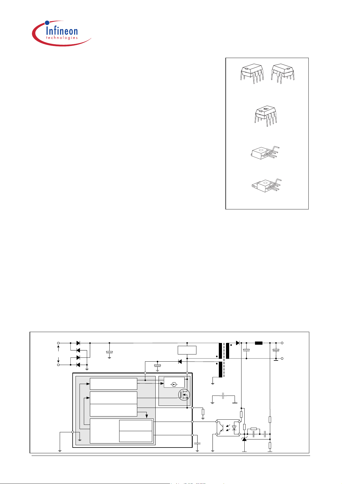
• Best in class in DIP7, DIP8, TO220/I2Pak packages
• Active Burst Mode to reach the lowest Standby Power
Requirements < 100mW
• Protection features (Auto Restart Mode) to increase robustness and
safety of the system
• Adjustable Blanking Window for high load jumps to
increase system reliability
• Isolated drain package for TO220/I2Pak
• Wide creepage distance for DIP7/TO220/I2Pak
• Wide power class of products for various applications
• Pb-free lead plating for all packages; RoHS compliant
CoolSET™-F3
PG-DIP-7-1
P-DIP-7-1
PG-DIP-8-6
P-DIP-8-4, -6
PG-TO220-6-46 (I2Pak)
PG-TO220-6-47
Features
• 650V avalanche rugged CoolMOS™ with built in
switchable Startup Cell
• Active Burst Mode for lowest Standby Power
@ light load controlled by Feedback signal
• Fast load jump response in Active Burst Mode
• 67/100 kHz fixed switching frequency
• Auto Restart Mode for Overtemperature Detection
• Auto Restart Mode for Overvoltage Detection
• Auto Restart Mode for Overload and Open Loop
• Auto Restart Mode for VCC Undervoltage
• Blanking Window for short duration high current
• User defined Soft Start
• Minimum of external components required
• Max Duty Cycle 72%
• Overall tolerance of Current Limiting < ±5%
• Internal PWM Leading Edge Blanking
• Soft driving for low EMI
Typical Application
C
85 ... 270 VAC
Power Management
Bulk
VCC
Description
The new generation CoolSET™-F3 provides Active Burst Mode
to reach the lowest Standby Power Requirements <100mW at no
load. As the controller is always active during Active Burst
Mode, there is an immediate response on load jumps without any
black out in the SMPS. In Active Burst Mode the ripple of the
output voltage can be reduced <1%. Furthermore, to increase the
robustness and safety of the system, the device enters into Auto
Restart Mode in the cases of Overtemperature, VCC
Overvoltage, Output Open Loop or Overload and VCC
Undervoltage. By means of the internal precise peak current
limitation, the dimension of the transformer and the secondary
diode can be lowered which leads to more cost efficiency. An
adjustable blanking window prevents the IC from entering Auto
Restart or Active Burst Mode unintentionally during high load
jumps. The CoolSET™-F3 family consists a wide power class
range of products for various applications.
+
Converter
DC Output
-
C
VCC
Startup Cell
Snubber
Drain
GND
PWM Controller
Current Mode
Precise Low Tolerance Peak
Current Limitation
Control
Unit
Active Burst Mode
Auto Restart Mode
Depl.
CoolMOS™
CoolSET™-F3
CS
FB
SoftS
R
Sense
C
SoftS
Version 2.0 3 24 Aug 2005
Overview
CoolSET™-F3
Type Package V
DS
F
OSC
1)
R
DSon
230VAC ±15%
2)
85-265 VAC
ICE3A0365 PG-DIP-8-6 650V 100kHz 6.45 22W 10W
ICE3A0565 PG-DIP-8-6 650V 100kHz 4.70 25W 12W
ICE3A1065 PG-DIP-8-6 650V 100kHz 2.95 32W 16W
ICE3A1565 PG-DIP-8-6 650V 100kHz 1.70 42W 20W
ICE3A2065 PG-DIP-8-6 650V 100kHz 0.92 57W 28W
ICE3A2565 PG-DIP-8-6 650V 100kHz 0.65 68W 33W
ICE3B0365 PG-DIP-8-6 650V 67kHz 6.45 22W 10W
ICE3B0565 PG-DIP-8-6 650V 67kHz 4.70 25W 12W
ICE3B1065 PG-DIP-8-6 650V 67kHz 2.95 32W 16W
ICE3B1565 PG-DIP-8-6 650V 67kHz 1.70 42W 20W
ICE3B2065 PG-DIP-8-6 650V 67kHz 0.92 57W 28W
ICE3B2565 PG-DIP-8-6 650V 67kHz 0.65 68W 33W
1)
typ @ T=25°C
2)
Calculated maximum input power rating at Ta=75°C, Tj=125°C and without copper area as heat sink.
Type Package V
DS
F
OSC
1)
R
DSon
230VAC ±15%
2)
85-265 VAC
ICE3A0565Z PG-DIP-7-1 650V 100kHz 4.70 25W 12W
ICE3A2065Z PG-DIP-7-1 650V 100kHz 0.92 57W 28W
1)
typ @ T=25°C
2)
Calculated maximum input power rating at Ta=75°C, Tj=125°C and without copper area as heat sink.
2)
2)
Version 2.0 4 24 Aug 2005

CoolSET™-F3
Type Package V
DS
F
OSC
1)
R
DSon
230VAC ±15%
2)
85-265 VAC
ICE3A2065I PG-TO-220-6-46 650V 100kHz 3.00 102W 50W
ICE3A3065I PG-TO-220-6-46 650V 100kHz 2.10 128W 62W
ICE3A3565I PG-TO-220-6-46 650V 100kHz 1.55 170W 83W
ICE3A5065I PG-TO-220-6-46 650V 100kHz 0.95 220W 105W
ICE3A5565I PG-TO-220-6-46 650V 100kHz 0.79 240W 120W
ICE3B2065I PG-TO-220-6-46 650V 67kHz 3.00 102W 50W
ICE3B3065I PG-TO-220-6-46 650V 67kHz 2.10 128W 62W
ICE3B3565I PG-TO-220-6-46 650V 67kHz 1.55 170W 83W
ICE3B5065I PG-TO-220-6-46 650V 67kHz 0.95 220W 105W
ICE3B5565I PG-TO-220-6-46 650V 67kHz 0.79 240W 120W
ICE3A2065P PG-TO-220-6-47 650V 100kHz 3.00 102W 50W
ICE3A3065P PG-TO-220-6-47 650V 100kHz 2.10 128W 62W
ICE3A3565P PG-TO-220-6-47 650V 100kHz 1.55 170W 83W
ICE3A5065P PG-TO-220-6-47 650V 100kHz 0.95 220W 105W
ICE3A5565P PG-TO-220-6-47 650V 100kHz 0.79 240W 120W
ICE3B2065P PG-TO-220-6-47 650V 67kHz 3.00 102W 50W
ICE3B3065P PG-TO-220-6-47 650V 67kHz 2.10 128W 62W
ICE3B3565P PG-TO-220-6-47 650V 67kHz 1.55 170W 83W
ICE3B5065P PG-TO-220-6-47 650V 67kHz 0.95 220W 105W
ICE3B5565P PG-TO-220-6-47 650V 67kHz 0.79 240W 120W
1)
typ @ T=25°C
2)
Calculated maximum continuous input power in an open frame design at Ta=50°C, Tj=125°C and R
(external heatsink)=2.7K/W
thCA
2)
Version 2.0 5 24 Aug 2005

Table of Contents Page
1 Pin Configuration and Functionality . . . . . . . . . . . . . . . . . . . . . . . . . . . . . . . . . . . 7
1.1 Pin Configuration with PG-DIP-8-6 . . . . . . . . . . . . . . . . . . . . . . . . . . . . . . . . . . . . . 7
1.2 Pin Configuration with PG-DIP-7-1 . . . . . . . . . . . . . . . . . . . . . . . . . . . . . . . . . . . . . 7
1.3 Pin Configuration with PG-TO220-6-46 . . . . . . . . . . . . . . . . . . . . . . . . . . . . . . . . . . 8
1.4 Pin Configuration with PG-TO220-6-47 . . . . . . . . . . . . . . . . . . . . . . . . . . . . . . . . . . 8
1.5 Pin Functionality . . . . . . . . . . . . . . . . . . . . . . . . . . . . . . . . . . . . . . . . . . . . . . . . . . . . 9
2 Representative Blockdiagram . . . . . . . . . . . . . . . . . . . . . . . . . . . . . . . . . . . . . . . . 10
3 Functional Description . . . . . . . . . . . . . . . . . . . . . . . . . . . . . . . . . . . . . . . . . . . . . 11
3.1 Introduction . . . . . . . . . . . . . . . . . . . . . . . . . . . . . . . . . . . . . . . . . . . . . . . . . . . . . . . 11
3.2 Power Management . . . . . . . . . . . . . . . . . . . . . . . . . . . . . . . . . . . . . . . . . . . . . . . . . 11
3.3 Startup Phase . . . . . . . . . . . . . . . . . . . . . . . . . . . . . . . . . . . . . . . . . . . . . . . . . . . . . . 12
3.4 PWM Section . . . . . . . . . . . . . . . . . . . . . . . . . . . . . . . . . . . . . . . . . . . . . . . . . . . . . . 13
3.4.1 Oscillator . . . . . . . . . . . . . . . . . . . . . . . . . . . . . . . . . . . . . . . . . . . . . . . . . . . . . . . 13
3.4.2 PWM-Latch FF1 . . . . . . . . . . . . . . . . . . . . . . . . . . . . . . . . . . . . . . . . . . . . . . . . . 13
3.4.3 Gate Driver . . . . . . . . . . . . . . . . . . . . . . . . . . . . . . . . . . . . . . . . . . . . . . . . . . . . . 13
3.5 Current Limiting . . . . . . . . . . . . . . . . . . . . . . . . . . . . . . . . . . . . . . . . . . . . . . . . . . . 14
3.5.1 Leading Edge Blanking . . . . . . . . . . . . . . . . . . . . . . . . . . . . . . . . . . . . . . . . . . . . 14
3.5.2 Propagation Delay Compensation . . . . . . . . . . . . . . . . . . . . . . . . . . . . . . . . . . . . 14
3.6 Control Unit . . . . . . . . . . . . . . . . . . . . . . . . . . . . . . . . . . . . . . . . . . . . . . . . . . . . . . . 15
3.6.1 Adjustable Blanking Window . . . . . . . . . . . . . . . . . . . . . . . . . . . . . . . . . . . . . . . 15
3.6.2 Active Burst Mode . . . . . . . . . . . . . . . . . . . . . . . . . . . . . . . . . . . . . . . . . . . . . . . 16
3.6.2.1 Entering Active Burst Mode . . . . . . . . . . . . . . . . . . . . . . . . . . . . . . . . . . . . . . 16
3.6.2.2 Working in Active Burst Mode . . . . . . . . . . . . . . . . . . . . . . . . . . . . . . . . . . . 16
3.6.2.3 Leaving Active Burst Mode . . . . . . . . . . . . . . . . . . . . . . . . . . . . . . . . . . . . . . 16
3.6.3 Protection Mode (Auto Restart Mode) . . . . . . . . . . . . . . . . . . . . . . . . . . . . . . . . 17
CoolSET™-F3
4 Electrical Characteristics . . . . . . . . . . . . . . . . . . . . . . . . . . . . . . . . . . . . . . . . . . . 19
4.1 Absolute Maximum Ratings . . . . . . . . . . . . . . . . . . . . . . . . . . . . . . . . . . . . . . . . . . 19
4.2 Operating Range . . . . . . . . . . . . . . . . . . . . . . . . . . . . . . . . . . . . . . . . . . . . . . . . . . . 23
4.3 Characteristics . . . . . . . . . . . . . . . . . . . . . . . . . . . . . . . . . . . . . . . . . . . . . . . . . . . . . 23
4.3.1 Supply Section 1 . . . . . . . . . . . . . . . . . . . . . . . . . . . . . . . . . . . . . . . . . . . . . . . . . 23
4.3.2 Supply Section 2 . . . . . . . . . . . . . . . . . . . . . . . . . . . . . . . . . . . . . . . . . . . . . . . . . 24
4.3.3 Internal Voltage Reference . . . . . . . . . . . . . . . . . . . . . . . . . . . . . . . . . . . . . . . . . 25
4.3.4 PWM Section . . . . . . . . . . . . . . . . . . . . . . . . . . . . . . . . . . . . . . . . . . . . . . . . . . . 25
4.3.5 Control Unit . . . . . . . . . . . . . . . . . . . . . . . . . . . . . . . . . . . . . . . . . . . . . . . . . . . . . 26
4.3.6 Current Limiting . . . . . . . . . . . . . . . . . . . . . . . . . . . . . . . . . . . . . . . . . . . . . . . . . 26
4.3.7 CoolMOS™ Section . . . . . . . . . . . . . . . . . . . . . . . . . . . . . . . . . . . . . . . . . . . . . . 27
5 Outline Dimension . . . . . . . . . . . . . . . . . . . . . . . . . . . . . . . . . . . . . . . . . . . . . . . . . 29
Version 2.0 6 24 Aug 2005
CoolSET™-F3
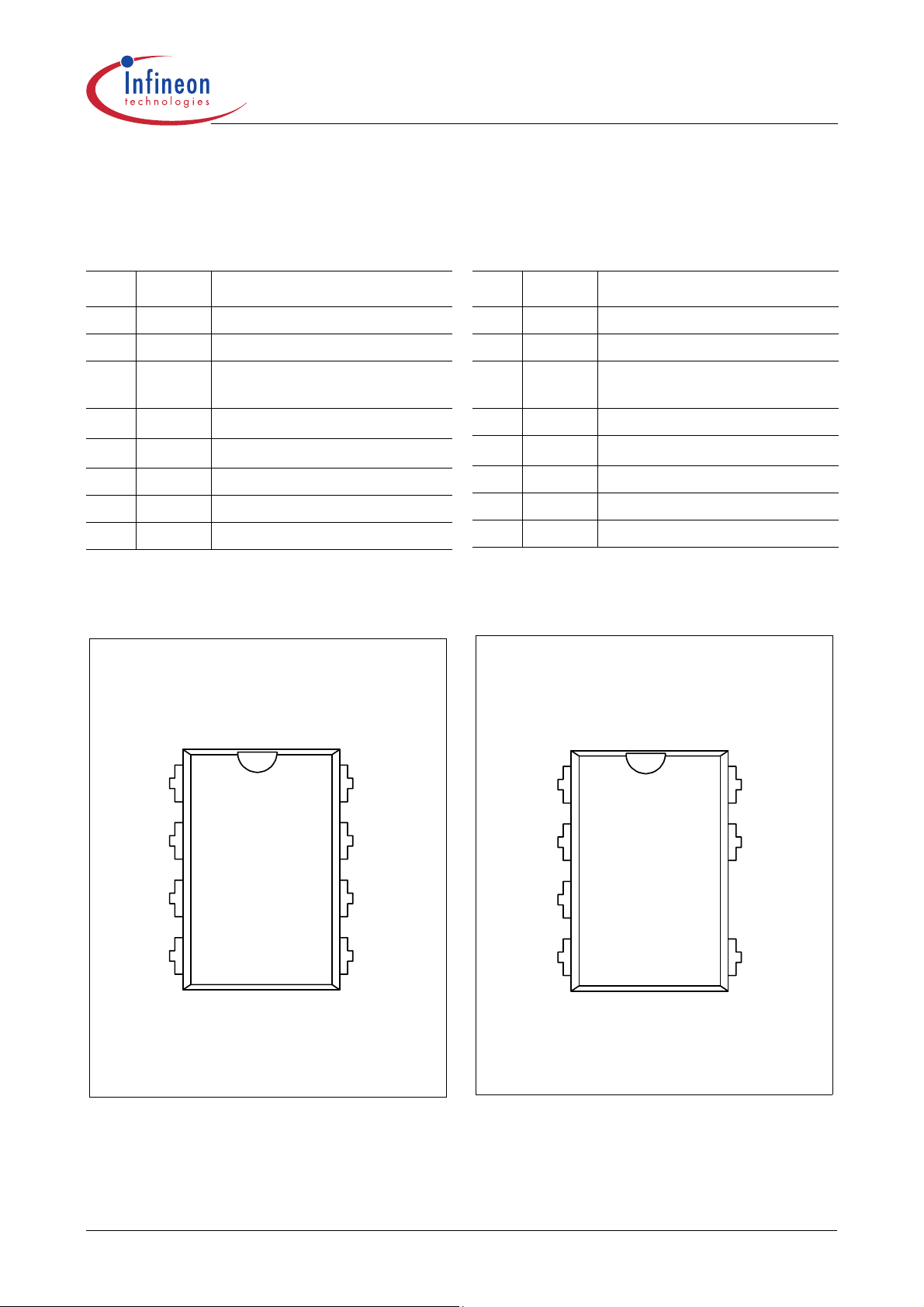
Pin Configuration and Functionality
1 Pin Configuration and Functionality
1.1 Pin Configuration with PG-DIP-8-6
Pin Symbol Function
1 SoftS Soft-Start
2 FB Feedback
3 CS Current Sense/
4Drain
5Drain
6 n.c. Not Connected
7 VCC Controller Supply Voltage
8 GND Controller Ground
1)
at Tj = 110°C
1)
Depl. CoolMOS™ Source
650V
1)
Depl. CoolMOS™ Drain
650V
1)
Depl. CoolMOS™ Drain
650V
1.2 Pin Configuration with PG-DIP-7-1
Pin Symbol Function
1 SoftS Soft-Start
2 FB Feedback
3 CS Current Sense/
4 n.c. Not connected
5Drain
---
7 VCC Controller Supply Voltage
8 GND Controller Ground
1)
at Tj = 110°C
1)
Depl. CoolMOS™ Source
650V
1)
Depl. CoolMOS™ Drain
650V
FB
CS
Drain
Package PG-DIP-8-6
1
2
3
4
8
7
6
5
GNDSoftS
VCC
n.c.
Drain
Package PG-DIP-7-1
1
FB
CS
n.c. Drain
2
3
4
8
7
5
GNDSoftS
VCC
Figure 1 Pin Configuration PG-DIP-8-6(top view)
Note: Pin 4 and 5 are shorted within the DIP 8 package.
Figure 2 Pin Configuration PG-DIP-7-1(top view)
Version 2.0 7 24 Aug 2005
CoolSET™-F3
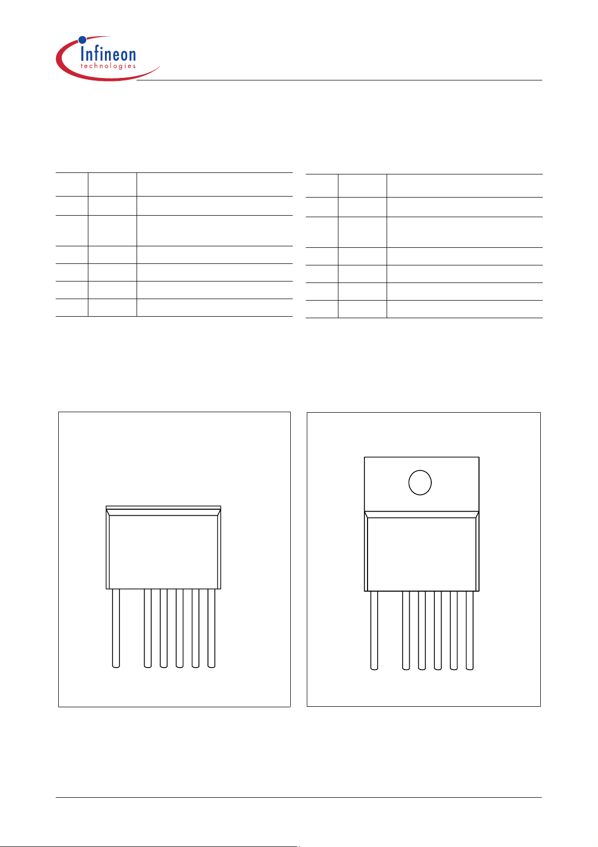
1.3 Pin Configuration with PG-TO220-6-46
Pin Symbol Function
1Drain
3 CS Current Sense/
4 GND Controller Ground
5 VCC Controller Supply Voltage
6 SoftS Soft-Start
7 FB Feedback
1)
at Tj = 110°C
1)
650V
Depl. CoolMOS™ Drain
1)
650V
Depl. CoolMOS™ Source
Pin Configuration and Functionality
1.4 Pin Configuration with PG-TO220-6-47
Pin Symbol Function
1Drain
3 CS Current Sense/
4 GND Controller Ground
5 VCC Controller Supply Voltage
6 SoftS Soft-Start
7 FB Feedback
1)
at Tj = 110°C
1)
650V
Depl. CoolMOS™ Drain
1)
Depl. CoolMOS™ Source
650V
Package PG-TO220-6-46 (I2Pak)
1
234567
Drain
CS
GND
VCC
SoftS
FB
Package PG-TO220-6-47
1
234567
Drain
CS
GND
VCC
SoftS
FB
Figure 3 Pin Configuration PG-TO220-6-46 I2Pak (front
view)
Figure 4 Pin Configuration PG-TO220-6-47
(front view)
Version 2.0 8 24 Aug 2005

CoolSET™-F3
1.5 Pin Functionality
SoftS (Soft Start & Auto Restart Control)
The SoftS pin combines the functions of Soft Start during
Start Up and error detection for Auto Restart Mode. These
functions are implemented and can be adjusted by means of
an external capacitor at SoftS to ground. This capacitor also
provides an adjustable blanking window for high load jumps,
before the IC enters into Auto Restart Mode.
FB (Feedback)
The information about the regulation is provided by the FB
Pin to the internal Protection Unit and to the internal PWMComparator to control the duty cycle. The FB-Signal
controls in case of light load the Active Burst Mode of the
controller.
CS (Current Sense)
The Current Sense pin senses the voltage developed on the
series resistor inserted in the source of the integrated Depl.
CoolMOS™. If CS reaches the internal threshold of the
Current Limit Comparator, the Driver output is immediately
switched off. Furthermore the current information is
provided for the PWM-Comparator to realize the Current
Mode.
Pin Configuration and Functionality
Drain (Drain of integrated Depl. CoolMOS™)
Pin Drain is the connection to the Drain of the internal Depl.
CoolMOS
VCC (Power supply)
The VCC pin is the positive supply of the IC. The operating
range is between 8.5V and 21V.
GND (Ground)
The GND pin is the ground of the controller.
TM
.
Version 2.0 9 24 Aug 2005
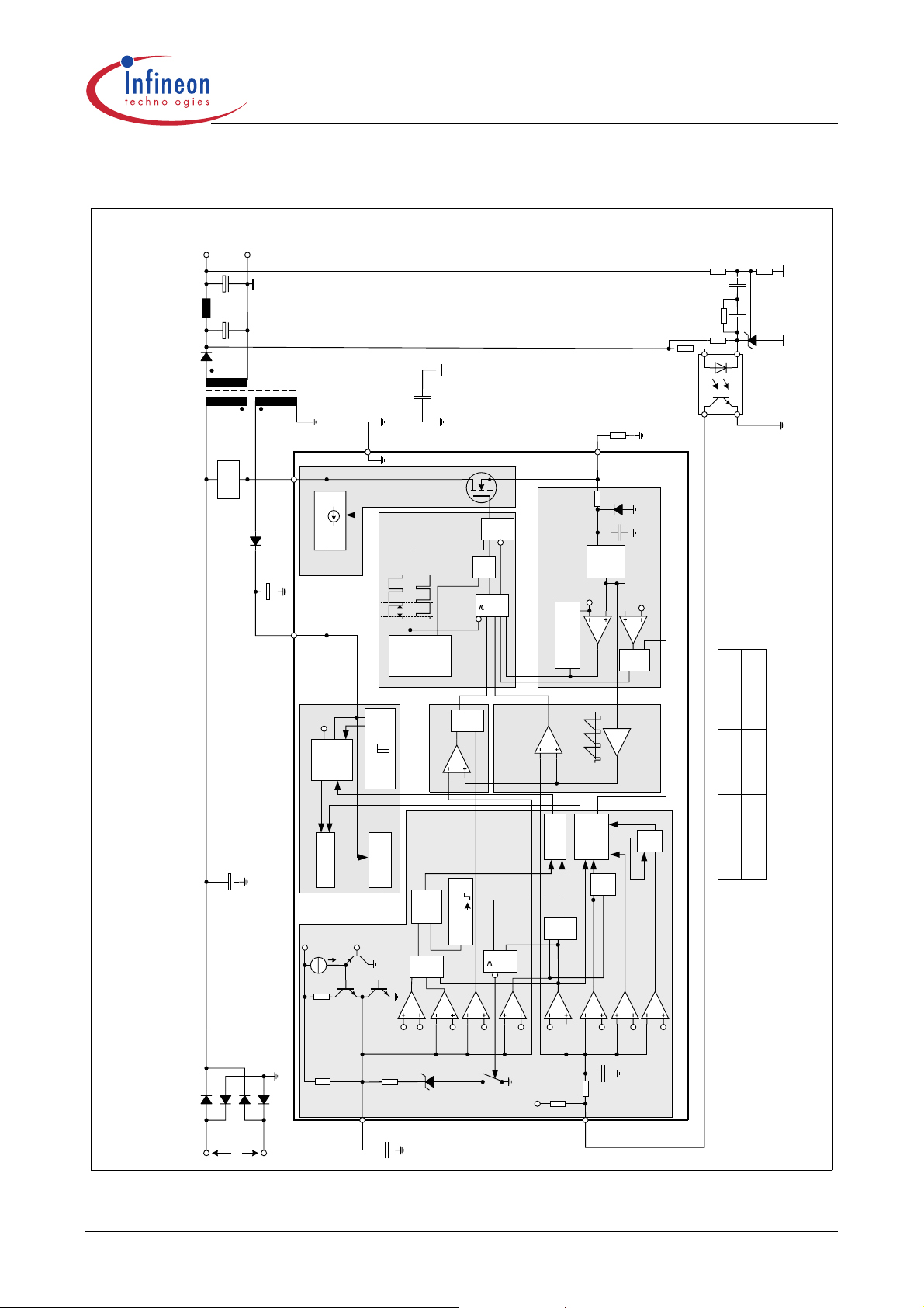
2 Representative Blockdiagram
-
+
OUT
V
Converter
DC Output
GND
CoolSET™-F3
Representative Blockdiagram
Sense
R
CS
Snubber
&
G9
Gate
Startup Cell
Depl. CoolMOS™
VCC
C
VCC Drain
6.5V
Voltage
Reference
Bulk
C
Internal Bias
Power Management
6.5V
PWM
Section
0.72
max
Duty Cycle Max
Duty Cycle
Oscillator
15V
8.5V
Undervoltage Lockout
Reset
Power-Down
Spike
1V
T3
&
Driver
Q
FF1
S
R
1
G8
Clock
&
G7
Soft-Start
Comparator
C7
Soft Start
8.0us
Blanking
>140°C
j
T
Thermal Shutdown
G1
PWM
C8
Comparator
Mode
Auto Restart
&
1
G2
D1
10k
1pF
Current Limiting
Edge
220ns
Leading
Blanking
csth
V
Compensation
Propagation-Delay
0.257V
C10
C12
&
G10
ICE3Bxxxx
x3.7
0.85V
PWM OP
Current Mode
&
Mode
Active Burst
&
G5
G11
G6
ICE3Axxxx
100kHz 67kHz
OSC
f
T1
T2
3.25k
SoftS
R
85 ... 270 VAC
5k
SoftS
C
SoftS
C11
C1
17V
VCC
C2
C3
4.0V
4.0V
4.4V
5.4VC44.8V
S1
6.5V
C5
C6a
C6b
3.4V
4.0V
1.32V
FB
5k
R
10pF
Control Unit
CoolSET™-F3
FB
Figure 5 Representative Blockdiagram
Version 2.0 10 24 Aug 2005
CoolSET™-F3
3 Functional Description
All values which are used in the functional description are
typical values. For calculating the worst cases the min/max
values which can be found in section 4 Electrical
Characteristics have to be considered.
3.1 Introduction
CoolSET™-F3 is the further development of the
CoolSET™-F2 to meet the requirements for the lowest
Standby Power at minimum load and no load conditions. A
new fully integrated Standby Power concept is implemented
into the IC in order to keep the application design easy.
Compared to CoolSET™-F2 no further external parts are
needed to achieve the lowest Standby Power. An intelligent
Active Burst Mode is used for this Standby Mode. After
entering this mode there is still a full control of the power
conversion by the secondary side via the same optocoupler
that is used for the normal PWM control. The response on
load jumps is optimized. The voltage ripple on V
minimized. V
is further on well controlled in this mode.
out
The usually external connected RC-filter in the feedback line
after the optocoupler is integrated in the IC to reduce the
external part count.
Furthermore a high voltage Startup Cell is integrated into the
IC which is switched off once the Undervoltage Lockout onthreshold of 15V is exceeded. This Startup Cell is part of the
integrated Depl. CoolMOS™. The external startup resistor is
no longer necessary as this Startup Cell is connected to the
Drain. Power losses are therefore reduced. This increases the
efficiency under light load conditions drastically.
The Soft-Start capacitor is also used for providing an
adjustable blanking window for high load jumps. During this
time window the overload detection is disabled. With this
concept no further external components are necessary to
adjust the blanking window.
An Auto Restart Mode is implemented in the IC to reduce the
average power conversion in the event of malfunction or
unsafe operating condition in the SMPS system. This feature
increases the system’s robustness and safety which would
otherwise lead to a destruction of the SMPS. Once the
malfunction is removed, normal operation is automatically
initiated after the next Start Up Phase.
The internal precise peak current limitation reduces the costs
for the transformer and the secondary diode. The influence
of the change in the input voltage on the power limitation can
be avoided together with the integrated Propagation Delay
Compensation. Therefore the maximum power is nearly
independent on the input voltage which is required for wide
range SMPS. There is no need for an extra over-sizing of the
SMPS, e.g. the transformer or the secondary diode.
out
is
Functional Description
3.2 Power Management
VCC Drain
Startup Cell
Depl. CoolMOS™
Power
Undervoltage Lockout
8.5V
15V
T1
SoftS
Figure 6 Power Management
The Undervoltage Lockout monitors the external supply
voltage V
. When the SMPS is plugged to the main line
VCC
the internal Startup Cell is biased and starts to charge the
external capacitor C
which is connected to the VCC pin.
VCC
This VCC charge current which is provided by the Startup
Cell from the Drain pin is 1.05mA. When V
on-threshold V
=15V the internal voltage reference and
CCon
bias circuit are switched on. Then the Startup Cell is
switched off by the Undervoltage Lockout and therefore no
power losses present due to the connection of the Startup
Cell to the Drain voltage. To avoid uncontrolled ringing at
switch-on a hysteresis is implemented. The switch-off of the
controller can only take place after Active Mode was entered
and V
falls below 8.5V.
VCC
The maximum current consumption before the controller is
activated is about 160µA.
When V
falls below the off-threshold V
VCC
internal reference is switched off and the Power Down reset
let T1 discharging the soft-start capacitor C
Thus it is ensured that at every startup cycle the voltage ramp
at pin SoftS starts at zero.
Management
Internal Bias
Voltage
Reference
Auto Restart
Mode
Active Burst
Mode
VCC
SoftS
6.5V
exceeds the
=8.5V the
CCoff
at pin SoftS.
Version 2.0 11 24 Aug 2005
CoolSET™-F3
The internal Voltage Reference is switched off if Auto
Restart Mode is entered. The current consumption is then
reduced to 300µA.
Once the malfunction condition is removed, this block will
then turn back on. The recovery from Auto Restart Mode
does not require disconnecting the SMPS from the AC line.
When Active Burst Mode is entered, the internal Bias is
switched off in order to reduce the current consumption to
below 1.05mA while keeping the Voltage Reference active
as this is necessary in this mode.
3.3 Startup Phase
6.5V
3.25kΩ
R
Soft S
T2
T3
1V
SoftS
Functional Description
Figure 7). This maximum charge current in the very first
stage when V
V
Sof tS
5.4V
4V
1V
DC
max
DC
1
DC
2
is below 1V, is limited to 1.32mA.
SoftS
max. Startup Phase
max. Soft Start Phase
t
C
Soft S
4V
0.85V
Soft St ar t
C7
C2
PWM OP
Soft-Start
Comparator
&
G7
x3.7
Gate Driver
CS
Figure 7 Soft Start
At the beginning of the Startup Phase, the IC provides a Soft
Start duration whereby it controls the maximum primary
current by means of a duty cycle limitation. A signal V
which is generated by the external capacitor C
combination with the internal pull up resistor R
determines the duty cycle until V
When the Soft Start begins, C
exceeds 4V.
SoftS
is immediately charged up
SoftS
Softs
SoftS
in
SoftS
to approx. 1V by T2. Therefore the Soft Start Phase takes
place between 1V and 4V. Above V
longer duty cycle limitation DC
max
= 4V there is no
SoftsS
which is controlled by
comparator C7 since comparator C2 blocks the gate G7 (see
t1 t2
Figure 8 Startup Phase
By means of this extra charge stage, there is no delay in the
beginning of the Startup Phase when there is still no
switching. Furthermore Soft Start is finished at 4V to have
faster the maximum power capability. The duty cycles DC
and DC2 are depending on the mains and the primary
inductance of the transformer. The limitation of the primary
current by DC
to a maximum primary current which is limited by the
internal Current Limiting with CS = 1V. Therefore the
maximum Startup Phase is divided into a Soft Start Phase
until t1 and a phase from t1 until t2 where maximum power
is provided if demanded by the FB signal.
,
is related to V
2
= 4V. But DC1 is related
SoftS
t
1
Version 2.0 12 24 Aug 2005
CoolSET™-F3
3.4 PWM Section
0.72
Oscillator
Duty Cycle
max
Clo ck
Soft Start
Comparator
PWM
Comparator
Current
Limiti ng
Figure 9 PWM Section
1
G8
Functional Description
3.4.3 Gate Driver
PWM Secti on
VCC
PWM-Latch
1
Gat e
FF1
CoolMOS™
Q
Gate Dr iver
&
G9
Internal
CoolMOS™
Gat e
Gate Driver
Figure 10 Gate Driver
The driver-stage is optimized to minimize EMI and to
provide high circuit efficiency. This is done by reducing the
S
R
switch on slope when exceeding the internal CoolMOS™
threshold. This is achieved by a slope control of the rising
edge at the driver’s output (see Figure 11).
3.4.1 Oscillator
The oscillator generates a fixed frequency. The switching
frequency of ICE3Axx65x is f
ICE3Bxx65x f
= 67kHz. A resistor, a capacitor and a
OSC
= 100kHz and for
OSC
current source and current sink which determine the
frequency are integrated. The charging and discharging
current of the implemented oscillator capacitor are internally
trimmed, in order to achieve a very accurate switching
frequency. The ratio of controlled charge to discharge
current is adjusted to reach a maximum duty cycle limitation
of D
=0.72.
max
3.4.2 PWM-Latch FF1
The oscillator clock output provides a set pulse to the PWMLatch when initiating the internal CoolMOS™ conduction.
After setting the PWM-Latch can be reset by the PWM
comparator, the Soft Start comparator or the Current-Limit
comparator. In case of resetting, the driver is shut down
immediately.
(internal) V
5V
Gate
ca. t = 130ns
t
Figure 11 Gate Rising Slope
Thus the leading switch on spike is minimized. When the
integrated CoolMOS™ is switched off, the falling shape of
the driver is slowed down when reaching 2V to prevent an
overshoot below ground. Furthermore the driver circuit is
designed to eliminate cross conduction of the output stage.
During powerup when VCC is below the undervoltage
lockout threshold V
low to disable power transfer to the seconding side.
, the output of the Gate Driver is
VCCoff
Version 2.0 13 24 Aug 2005

CoolSET™-F3
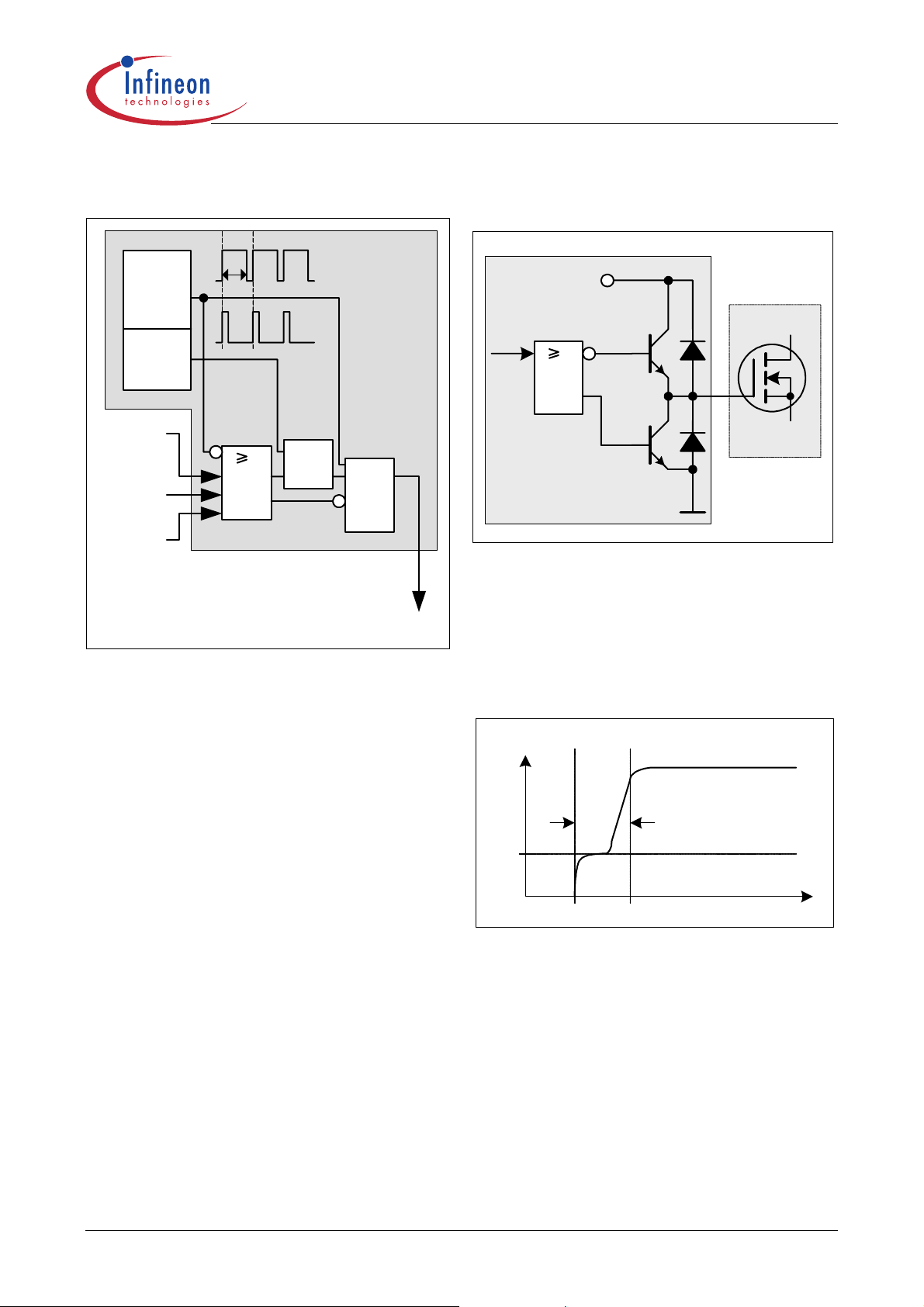
3.5 Current Limiting
PWM Latch
FF1
Propagation-Delay
Compensati on
C10
PWM-OP
&
G10
Acti ve Bur st
Mode
C12
10k
V
csth
0.257V
D1
Current Li miting
Leading
Edge
Blanking
220ns
1pF
Functional Description
3.5.1 Leading Edge Blanking
V
Sense
V
csth
Figure 13 Leading Edge Blanking
Each time when the internal CoolMOS™ is switched on, a
leading edge spike is generated due to the primary-side
capacitances and secondary-side rectifier reverse recovery
time. This spike can cause the gate drive to switch off
unintentionally. To avoid a premature termination of the
switching pulse, this spike is blanked out with a time
constant of t
= 220ns. During this time, the gate drive will
LEB
not be switched off.
t
LEB
= 220ns
t
CS
Figure 12 Current Limiting Block
There is a cycle by cycle Current Limiting realized by the
Current-Limit comparator C10 to provide an overcurrent
detection. The source current of the internal CoolMOS™ is
sensed via an external sense resistor R
the source current is transformed to a sense voltage
R
Sense
V
which is fed into the pin CS. If the voltage V
Sense
exceeds the internal threshold voltage V
C10 immediately turns off the gate drive by resetting the
PWM Latch FF1. A Propagation Delay Compensation is
added to support the immediate shut down without delay of
the internal CoolMOS™ in case of Current Limiting. The
influence of the AC input voltage on the maximum output
power can thereby be avoided.
To prevent the Current Limiting from distortions caused by
leading edge spikes a Leading Edge Blanking is integrated in
the current sense path for the comparators C10, C12 and the
PWM-OP.
The output of comparator C12 is activated by the Gate G10
if Active Burst Mode is entered. Once activated the current
limiting is thereby reduced to 0.257V. This voltage level
determines the power level when the Active Burst Mode is
left if there is a higher power demand.
. By means of
Sense
the comparator
csth
Sense
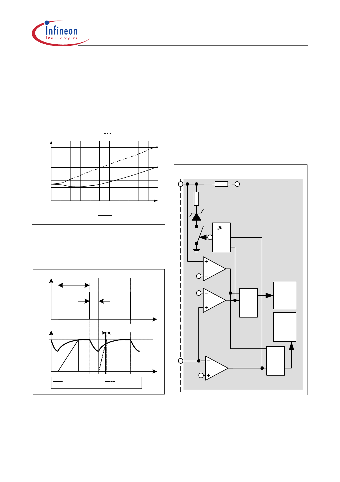
3.5.2 Propagation Delay Compensation
In case of overcurrent detection, the switch-off of the
internal CoolMOS™ is delayed due to the propagation delay
of the circuit. This delay causes an overshoot of the peak
current I
which depends on the ratio of dI/dt of the peak
peak
current (see Figure 14).
Signal2Signal1
I
peak2
I
peak1
I
Limit
I
Sense
I
Overshoot2
t
Propagation Delay
I
Overshoot1
t
Figure 14 Current Limiting
The overshoot of Signal2 is bigger than of Signal1 due to the
steeper rising waveform. This change in the slope is
depending on the AC input voltage. Propagation Delay
Compensation is integrated to limit the overshoot
dependency on dI/dt of the rising primary current. That
means the propagation delay time between exceeding the
current sense threshold V
CoolMOS™ is compensated over temperature within a wide
range.
and the switch off of the internal
csth
Version 2.0 14 24 Aug 2005
CoolSET™-F3
Current Limiting is now possible in a very accurate way. E.g.
= 0.5A with R
I
peak
Compensation the current sense threshold is set to a static
voltage level V
csth
dI/dt = 0.4A/µs, that means dV
propagation delay time of i.e. t
then to an I
overshoot of 14.4%. By means of propagation
peak
delay compensation the overshoot is only about 2% (see
Figure 15).
V
1,3
1,25
1,2
1,15
Sense
1,1
V
1,05
1
0,95
0,9
0 0,2 0,4 0,6 0,8 1 1,2 1,4 1,6 1,8 2
Figure 15 Overcurrent Shutdown
The Propagation Delay Compensation is realized by means
of a dynamic threshold voltage V
of a steeper slope the switch off of the driver is earlier to
compensate the delay.
V
OSC
max. Duty Cycle
= 2. Without Propagation Delay
Sense
=1V. A current ramp of
/dt = 0.8V/µs, and a
Sense
Propagation Delay
dV
Sense
without c ompensation
with compensation
dt
(see Figure 16). In case
csth
=180ns leads
V
s
µ
Functional Description
3.6 Control Unit
The Control Unit contains the functions for Active Burst
Mode and Auto Restart Mode. The Active Burst Mode and
the Auto Restart Mode are combined with an Adjustable
Blanking Window which is depending on the external Soft
Start capacitor. By means of this Adjustable Blanking
Window, the IC avoids entering into these two modes
accidentally. Furthermore it also provides a certain time
whereby the overload detection is delayed. This delay is
useful for applications which normally works with a low
current and occasionally require a short duration of high
current.
3.6.1 Adjustable Blanking Window
SoftS
6.5V
R
SoftS
5kΩ
4.4V
1
S1
5.4V
G2
C3
off time
V
Sense
V
csth
Propagation Delay
Signal1 Signal2
Figure 16 Dynamic Voltage Threshold V
csth
4.8V
&
C4
G5
Auto
Res ta rt
Mode
Activ e
t
Bur st
Mode
&
FB
G6
C5
1.32V
t
Control Unit
Figure 17 Adjustable Blanking Window
V
is clamped at 4.4V by the closed switch S1 after the
SoftS
SMPS is settled. If overload occurs V
is exceeding 4.8V.
FB
Auto Restart Mode can’t be entered as the gate G5 is still
blocked by the comparator C3. But after V
has exceeded
FB
4.8V the switch S1 is opened via the gate G2. The external
Version 2.0 15 24 Aug 2005

CoolSET™-F3
Soft Start capacitor can now be charged further by the
integrated pull up resistor R
the gates G5 and G6 once V
Therefore there is no entering of Auto Restart Mode possible
during this charging time of the external capacitor C
same procedure happens to the external Soft Start capacitor
if a low load condition is detected by comparator C5 when
is falling below 1.32V. Only after V
V
FB
5.4V and V
is still below 1.32V Active Burst Mode is
FB
entered.
3.6.2 Active Burst Mode
The controller provides Active Burst Mode for low load
conditions at V
. Active Burst Mode increases
OUT
significantly the efficiency at light load conditions while
supporting a low ripple on V
jumps. During Active Burst Mode which is controlled only
by the FB signal the IC is always active and can therefore
immediately response on fast changes at the FB signal. The
Startup Cell is kept switched off to avoid increased power
losses for the self supply.
SoftS
5k
4.4V
S1
C3
5.4V
4.8V
C4
FB
1.32V
4.0V
3.4V
C5
C6a
C6b
. The comparator C3 releases
SoftS
R
SoftS
has exceeded 5.4V.
Softs
has exceeded
SoftS
and fast response on load
OUT
6.5V
Internal Bias
&
G6
&
G11
Control Unit
SoftS
Current
Limiting
G10
Active
Burst
Mode
. The
&
Functional Description
3.6.2.1 Entering Active Burst Mode
The FB signal is always observed by the comparator C5 if
the voltage level falls below 1.32V. In that case the switch S1
is released which allows the capacitor C
starting from the clamped voltage level at 4.4V in normal
operating mode. If V
exceeds 5.4V the comparator C3
SoftS
releases the gate G6 to enter the Active Burst Mode. The
time window that is generated by combining the FB and
SoftS signals with gate G6 avoids a sudden entering of the
Active Burst Mode due to large load jumps. This time
window can be adjusted by the external capacitor C
After entering Active Burst Mode a burst flag is set and the
internal bias is switched off in order to reduce the current
consumption of the IC down to approx. 1.05mA. In this Off
State Phase the IC is no longer self supplied so that therefore
C
has to provide the VCC current (see Figure 19).
VCC
Furthermore gate G11 is then released to start the next burst
cycle once V
has 3.4V exceeded.
FB
It has to be ensured by the application that the VCC remains
above the Undervoltage Lockout Level of 8.5V to avoid that
the Startup Cell is accidentally switched on. Otherwise
power losses are significantly increased. The minimum VCC
level during Active Burst Mode is depending on the load
conditions and the application. The lowest VCC level is
reached at no load conditions at V
OUT
3.6.2.2 Working in Active Burst Mode
After entering the Active Burst Mode the FB voltage rises as
V
starts to decrease due to the inactive PWM section.
OUT
Comparator C6a observes the FB signal if the voltage level
4V is exceeded. In that case the internal circuit is again
activated by the internal Bias to start with switching. As now
in Active Burst Mode the gate G10 is released the current
limit is only 0.257V to reduce the conduction losses and to
avoid audible noise. If the load at V
starting level for the Active Burst Mode the FB signal
decreases down to 3.4V. At this level C6b deactivates again
the internal circuit by switching off the internal Bias. The
gate G11 is released as after entering Active Burst Mode the
burst flag is set. If working in Active Burst Mode the FB
voltage is changing like a saw tooth between 3.4V and 4V
(see Figure 19).
3.6.2.3 Leaving Active Burst Mode
The FB voltage immediately increases if there is a high load
jump. This is observed by comparator C4. As the current
limit is ca. 26% during Active Burst Mode a certain load
jump is needed that FB can exceed 4.8V. At this time C4
resets the Active Burst Mode which also blocks C12 by the
to be charged
SoftS
.
is still below the
OUT
SoftS
.
Figure 18 Active Burst Mode
The Active Burst Mode is located in the Control Unit. Figure
18 shows the related components.
Version 2.0 16 24 Aug 2005

CoolSET™-F3
gate G10. Maximum current can now be provided to
stabilize V
V
FB
4.80V
4.00V
3.40V
1.32V
V
SoftS
5.40V
4.40V
V
CS
1.00V
0.257V
V
VCC
.
OUT
Enter ing Ac tive
Burst Mode
Blanking Window
Current limit level during
Active Burst Mode
Leaving Acti ve
Burst Mode
t
t
t
Functional Description
3.6.3 Protection Mode (Auto Restart Mode)
In order to increase the SMPS system’s robustness and
safety, the IC provides the Auto Restart Mode as a protection
feature. The Auto Restart Mode is entered upon detection of
the following faults in the system:
• VCC Overvoltage
• Overtemperature
•Overload
• Open Loop
• VCC Undervoltage
• Short Optocoupler
SoftS
C
Soft S
FB
R
Soft S
5k
VCC
17V
4.0V
4.8V
C1
C11
C4
4.4V
S1
6.5V
&
G1
Thermal Shutdown
Tj >140°C
Spike
Blanking
8.0us
&
G5
Contr ol Unit
Auto Restart
Mode
8.5V
I
VCC
7.2mA
1.05mA
V
OUT
Max . Ri ppl e < 1%
Figure 19 Signals in Active Burst Mode
C3
5.4V
Figure 20 Auto Restart Mode
The VCC voltage is observed by comparator C1 if 17V is
t
exceeded. The output of C1 is combined with both the output
of C11 which checks for SoftS<4.0V, and the output of C4
which checks for FB>4.8V. Therefore the overvoltage
detection is can only active during Soft Start
Phase(SoftS<4.0V) and when FB signal is outside the
operating range > 4.8V. This means any small voltage
overshoots of V
during normal operating cannot trigger
VCC
the Auto Restart Mode.
t
In order to ensure system reliability and prevent any false
activation, a blanking time is implemented before the IC can
enter into the Auto Restart Mode. The output of the VCC
overvoltage detection is fed into a spike blanking with a time
constant of 8.0µs.
The other fault detection which can result in the Auto Restart
Mode and has this 8.0µs blanking time is the
Overtemperature detection. This block checks for a junction
t
temperature of higher than 140°C for malfunction operation.
Once the Auto Restart Mode is entered, the internal Voltage
Reference is switched off in order to reduce the current
Volt age
Reference
Version 2.0 17 24 Aug 2005

CoolSET™-F3
consumption of the IC as much as possible. In this mode, the
average current consumption is only 300µA as the only
working block is the Undervoltage Lockout(UVLO) which
controls the Startup Cell by switching on/off at V
.
V
VCCoff
As there is no longer a self supply by the auxiliary winding,
VCC starts to drop. The UVLO switches on the integrated
Startup Cell when VCC falls below 8.5V. It will continue to
charge VCC up to 15V whereby it is switched off again and
the IC enters into the Start Up Phase.
As long as all fault conditions have been removed, the IC
will automatically power up as usual with switching cycle at
the GATE output after Soft Start duration. Thus the name
Auto Restart Mode.
Other fault detections which are active in normal operation
is the sensing for Overload, Open Loop and VCC
undervoltage conditions. In the first 2 cases, FB will rise
above 4.8V which will be observed by C4. At this time, S1
is released such that V
voltage of 4.4V. If V
C3, Auto Restart Mode is entered as both inputs of the gate
G5 are high.
This charging of the Soft Start capacitor from 4.4V to 5.4V
defines a blanking window which prevents the system from
entering into Auto Restart Mode un-intentionally during
large load jumps. In this event, FB will rise close to 6.5V for
a short duration before the loop regulates with FB less than
4.8V. This is the same blanking time window as for the
Active Burst Mode and can therefore be adjusted by the
external C
In the case of VCC undervoltage, ie. VCC falls below 8.5V,
the IC will be turn off with the Startup Cell charging VCC as
described earlier in this section. Once VCC is charged above
15V, the IC will start a new startup cycle. The same
procedure applies when the system is under Short
Optocoupler fault condition, as it will lead to VCC
undervoltage.
SoftS
.
can rise from its earlier clamp
SoftS
exceeds 5.4V which is observed by
SoftS
VCCon
Functional Description
/
Version 2.0 18 24 Aug 2005

CoolSET™-F3
Electrical Characteristics
4 Electrical Characteristics
Note: All voltages are measured with respect to ground (Pin 8). The voltage levels are valid if other ratings are not
violated.
4.1 Absolute Maximum Ratings
Note: Absolute maximum ratings are defined as ratings, which when being exceeded may lead to destruction of the
integrated circuit. For the same reason make sure, that any capacitor that will be connected to pin 7 (VCC) is
discharged before assembling the application circuit.
Parameter Symbol Limit Values Unit Remarks
min. max.
Drain Source Voltage
ICE3Axx65/xx65I/xx65P
ICE3Bxx65/xx65I/xx65P
Pulse drain current, t
limited by max. T
p
=150°C
j
ICE3x0365 I
ICE3x0565
ICE3A0565Z
ICE3x1065 I
ICE3x1565 I
ICE3x2065
ICE3A2065Z
ICE3x2565 I
ICE3x2065I
ICE3x2065P
ICE3x3065I
ICE3x3065P
ICE3x3565I
ICE3x3565P
V
DS
D_Puls1
I
D_Puls2
D_Puls3
D_Puls4
I
D_Puls5
D_Puls6
I
D_Puls7
I
D_Puls8
I
D_Puls9
-650VTj=110°C
-1.6A
-2.3A
-3.4A
-6.1A
-10.3A
-15.7A
-3.4A
-4.3A
-6.5A
ICE3x5065I
I
D_Puls10
-9.4A
ICE3x5065P
ICE3x5565I
I
D_Puls11
-10.7A
ICE3x5565P
Version 2.0 19 24 Aug 2005

CoolSET™-F3
Electrical Characteristics
Parameter Symbol Limit Values Unit Remarks
min. max.
Avalanche energy,
repetitive t
max. T
AR
=150°C
j
limited by
1)
ICE3x0365 E
ICE3x0565
ICE3A0565Z
ICE3x1065 E
ICE3x1565 E
ICE3x2065
ICE3A2065Z
ICE3x2565 E
ICE3x2065I
ICE3x2065P
ICE3x3065I
ICE3x3065P
ICE3x3565I
ICE3x3565P
ICE3x5065I
ICE3x5065P
ICE3x5565I
ICE3x5565P
E
E
E
E
E
E
E
AR1
AR2
AR3
AR4
AR5
AR6
AR7
AR8
AR9
AR10
AR11
-0.005mJ
-0.01mJ
-0.07mJ
-0.15mJ
-0.40mJ
-0.47mJ
-0.07mJ
-0.11mJ
-0.17mJ
-0.40mJ
-0.44mJ
Version 2.0 20 24 Aug 2005

CoolSET™-F3
Electrical Characteristics
Parameter Symbol Limit Values Unit Remarks
min. max.
Avalanche current,
repetitive t
max. T
AR
=150°C
j
limited by
ICE3x0365 I
ICE3x0565
ICE3A0565Z
ICE3x1065 I
ICE3x1565 I
ICE3x2065
ICE3A2065Z
ICE3x2565 I
ICE3x2065I
ICE3x2065P
ICE3x3065I
ICE3x3065P
ICE3x3565I
ICE3x3565P
ICE3x5065I
ICE3x5065P
ICE3x5565I
ICE3x5565P
AR1
I
AR2
AR3
AR4
I
AR5
AR6
I
AR7
I
AR8
I
AR9
I
AR10
I
AR11
-0.3A
-0.5A
-1.0A
-1.5A
-2.0A
-2.5A
-2.0A
-3.0A
-3.5A
-5.0A
-5.5A
1)
Repetitive avalanche causes additional power losses that can be calculated as PAV=EAR*f
Version 2.0 21 24 Aug 2005

CoolSET™-F3
Electrical Characteristics
Parameter Symbol Limit Values Unit Remarks
min. max.
Thermal Resistance
Junction-Ambient
Thermal Resistance
Junction-Case
ICE3x0365
ICE3x0565
ICE3x1065
ICE3x1565
ICE3x2065
ICE3x2565
ICE3A0565Z
ICE3x2065Z
ICE3x2065I
ICE3x3065I
ICE3x3565I
ICE3x5065I
ICE3x5565I
ICE3x2065P
ICE3x3065P
ICE3x3565P
ICE3x5065P
ICE3x5565P
ICE3x2065I
ICE3x2065P
ICE3x3065I
ICE3x3065P
R
R
R
R
R
R
thJA1
thJA2
thJA3
thJA4
thJC1
thJC2
90 K/W PG-DIP-8-6
96 K/W PG-DIP-7-1
103 K/W PG-TO220-6-46
Free standing without
heatsink
82 K/W PG-TO220-6-47
Free standing without
heatsink
3.30 K/W PG-TO220-6-46
PG-TO220-6-47
3.08 K/W PG-TO220-6-46
PG-TO220-6-47
ICE3x3565I
R
thJC3
ICE3x3565P
ICE3x5065I
R
thJC4
ICE3x5065P
ICE3x5565I
R
thJC5
ICE3x5565P
VCC Supply Voltage V
FB Voltage V
SoftS Voltage V
CS Voltage V
Junction Temperature T
Storage Temperature T
ESD Capability(incl. Drain Pin) V
1)
According to EIA/JESD22-A114-B (discharging a 100pF capacitor through a 1.5kΩ series resistor)
VCC
FB
SoftS
CS
j
S
ESD
-0.3 22 V
-0.3 6.5 V
-0.3 6.5 V
-0.3 6.5 V
-40 150 °C Controller & CoolMOS™
-55 150 °C
- 3 kV Human body model1)
2.94 K/W PG-TO220-6-46
PG-TO220-6-47
2.79 K/W PG-TO220-6-46
PG-TO220-6-47
2.75 K/W PG-TO220-6-46
PG-TO220-6-47
Version 2.0 22 24 Aug 2005

Electrical Characteristics
4.2 Operating Range
Note: Within the operating range the IC operates as described in the functional description.
Parameter Symbol Limit Values Unit Remarks
min. max.
CoolSET™-F3
VCC Supply Voltage V
Junction Temperature of Controller T
VCC
jCon
V
VCCoff
-25 130 °C Max value limited due to thermal shut
21 V
down of controller
Junction Temperature of
T
jCoolMOS
-25 150 °C
CoolMOS™
4.3 Characteristics
4.3.1 Supply Section 1
Note: The electrical characteristics involve the spread of values within the specified supply voltage and junction
temperature range T
25°C. If not otherwise stated, a supply voltage of V
Parameter Symbol Limit Values Unit Test Condition
Start Up Current I
VCC Charge Current I
Leakage Current of
Start Up Cell and CoolMOS™
Supply Current with
Inactive Gate
from – 25 °C to 130 °C. Typical values represent the median values, which are related to
J
= 15 V is assumed.
CC
min. typ. max.
VCCstart
VCCcharge1
I
VCCcharge2
I
StartLeak
I
VCCsup1
- 160 220 µA V
0.55 1.05 1.60 mA V
-0.88-mAV
-0.250µA V
-5.57.0mA
VCC
VCC
VCC
VCC
at T
=14V
= 0V
=14V
=16V, V
=100°C
j
Drain
= 450V
Supply Current in
Auto Restart Mode with
I
VCCrestart
- 300 - µA IFB = 0
I
= 0
Softs
Inactive Gate
Supply Current in
Active Burst Mode
with Inactive Gate
VCC Turn-On Threshold
VCC Turn-Off Threshold
VCC Turn-On/Off Hysteresis
I
VCCburst1
I
VCCburst2
V
VCCon
V
VCCoff
V
VCChys
- 1.05 1.25 mA V
- 0.95 1.15 mA V
14.2
8.0
-
15.0
8.5
6.5
15.8
9.0
-
V
V
V
VCC
V
= 3.7V, V
FB
VCC
V
= 3.7V, V
FB
=15V
= 9.5V
SoftS
SoftS
= 4.4V
= 4.4V
Version 2.0 23 24 Aug 2005

CoolSET™-F3
Electrical Characteristics
4.3.2 Supply Section 2
Parameter Symbol Limit Values Unit Test Condition
min. typ. max.
Supply Current
with Active Gate
Supply Current
with Active Gate
ICE3A0365 I
ICE3B0365 I
ICE3A0565
ICE3A0565Z
ICE3B0565 I
ICE3A1065 I
ICE3B1065 I
ICE3A1565 I
ICE3B1565 I
ICE3A2065
ICE3A2065Z
ICE3B2065 I
ICE3A2565 I
ICE3B2565 I
ICE3A2065I
ICE3A2065P
ICE3B2065I
ICE3B2065P
ICE3A3065I
ICE3A3065P
VCCsup2
VCCsup2
I
VCCsup2
VCCsup2
VCCsup2
VCCsup2
VCCsup2
VCCsup2
I
VCCsup2
VCCsup2
VCCsup2
VCCsup2
I
VCCsup2
I
VCCsup2
I
VCCsup2
-5.67.1mAV
-5.57.0mA
I
SoftS
FB
-5.77.2mA
-5.67.1mA
-5.97.5mA
-5.77.2mA
-6.38.0mA
-6.07.6mA
-7.18.9mA
-6.58.2mA
- 8.1 10.2 mA
-7.29.0mA
-5.97.5mAV
I
SoftS
FB
-5.77.2mA
-6.17.7mA
= 4.4V
= 0
= 4.4V
= 0
ICE3B3065I
ICE3B3065P
ICE3A3565I
ICE3A3565P
ICE3B3565I
ICE3B3565P
ICE3A5065I
ICE3A5065P
ICE3B5065I
ICE3B5065P
ICE3A5565I
ICE3A5565P
ICE3B5565I
ICE3B5565P
I
VCCsup2
I
VCCsup2
I
VCCsup2
I
VCCsup2
I
VCCsup2
I
VCCsup2
I
VCCsup2
-5.97.4mA
-6.48.0mA
-6.07.6mA
-7.29.0mA
-6.68.3mA
-7.69.5mA
-6.88.5mA
Version 2.0 24 24 Aug 2005

CoolSET™-F3
Electrical Characteristics
4.3.3 Internal Voltage Reference
Parameter Symbol Limit Values Unit Test Condition
min. typ. max.
Trimmed Reference Voltage V
REF
6.37 6.50 6.63 V measured at pin FB
= 0
I
FB
4.3.4 PWM Section
Parameter Symbol Limit Values Unit Test Condition
min. typ. max.
Fixed Oscillator
Frequency
ICE3Axx65
ICE3Axx65Z
ICE3Axx65I
ICE3Axx65P
Fixed Oscillator
Frequency
ICE3Bxx65
ICE3Bxx65I
ICE3Bxx65P
Max. Duty Cycle D
Min. Duty Cycle D
PWM-OP Gain A
Voltage Ramp Max Level V
Operating Range Min Level V
V
FB
f
OSC1
f
OSC2
f
OSC1
f
OSC2
max
min
V
Max-Ramp
FBmin
92 100 108 kHz
94 100 106 kHz Tj = 25°C
61 67 73 kHz
63 67 71 kHz Tj = 25°C
0.67 0.72 0.77
0- - VFB < 0.3V
3.5 3.7 3.9
-0.85-V
0.3 0.7 - V
V
Operating Range Max level V
FB
FB Pull-Up Resistor R
SoftS Pull-Up Resistor R
1)
The parameter is not subjected to production test - verified by design/characterization
FBmax
FB
SoftS
- - 4.75 V CS=1V, limited by
16 20 27 kΩ
39 50 62 kΩ
Comparator C4
1)
Version 2.0 25 24 Aug 2005
CoolSET™-F3
Electrical Characteristics
4.3.5 Control Unit
Parameter Symbol Limit Values Unit Test Condition
min. typ. max.
Deactivation Level for SoftS
Comparator C7 by C2
Clamped V
Voltage during
SoftS
Normal Operating Mode
Activation Limit of
Comparator C3
SoftS Startup Current I
Over Load & Open Loop Detection
Limit for Comparator C4
Active Burst Mode Level for
Comparator C5
Active Burst Mode Level for
Comparator C6a
Active Burst Mode Level for
Comparator C6b
Overvoltage Detection Limit V
Thermal Shutdown
1)
Spike Blanking t
V
SoftSC2
V
SoftSclmp
V
SoftSC3
SoftSstart
V
FBC4
V
FBC5
V
FBC6a
V
FBC6b
VCCOVP
T
jSD
Spike
3.85 4.00 4.15 V VFB > 5V
4.23 4.40 4.57 V VFB = 4V
5.20 5.40 5.60 V VFB > 5V
-1.3-mAV
4.62 4.80 4.98 V V
1.23 1.30 1.37 V V
SoftS
SoftS
SoftS
= 0V
> 5.6V
> 5.6V
3.85 4.00 4.15 V After Active Burst Mode
is entered
3.25 3.40 3.55 V After Active Burst Mode
is entered
16.1 17.1 18.1 V VFB > 5V
< 4.0V
V
SoftS
130 140 150 °C
-8.0-µs
1)
The parameter is not subjected to production test - verified by design/characterization
Note: The trend of all the voltage levels in the Control Unit is the same regarding the deviation except V
VCCOVP
4.3.6 Current Limiting
Parameter Symbol Limit Values Unit Test Condition
min. typ. max.
Peak Current Limitation
(incl. Propagation Delay)
Peak Current Limitation during
V
csth
V
CS2
0.97 1.02 1.07 V dV
0.232 0.257 0.282 V
/ dt = 0.6V/µs
sense
(see Figure 16)
Active Burst Mode
Leading Edge Blanking t
CS Input Bias Current I
LEB
CSbias
- 220 - ns V
-1.0 -0.2 0 µA V
SoftS
CS
= 4.4V
=0V
and V
VCCPD
Version 2.0 26 24 Aug 2005

CoolSET™-F3
Electrical Characteristics
4.3.7 CoolMOS™ Section
Parameter Symbol Limit Values Unit Test Condition
min. typ. max.
Drain Source Breakdown Voltage
ICE3Axx65/xx65I/xx65P
ICE3Bxx65/xx65I/xx65P
Drain Source
On-Resistance
ICE3A0365
ICE3B0365
ICE3A0565
ICE3A0565Z
ICE3B0565
ICE3A1065
ICE3B1065
ICE3A1565
ICE3B1565
ICE3A2065
ICE3A2065Z
ICE3B2065
ICE3A2565
ICE3B2565
Drain Source
On-Resistance
ICE3A2065I
ICE3A2065P
ICE3B2065I
ICE3B2065P
V
(BR)DSS
R
DSon1
R
DSon2
R
DSon3
R
DSon4
R
DSon5
R
DSon6
R
DSon7
600
650
-
-
-
-
-
-
-
-
-
-
-
-
-
-
-
-
6.45
13.7
4.70
10.0
2.95
6.6
1.70
3.57
0.92
1.93
0.65
1.37
3.00
6.6
-
-
7.50
17.0
5.44
12.5
3.42
7.56
1.96
4.12
1.05
2.22
0.75
1.58
3.47
7.63
V
V
Ω
Ω
Tj = 25°C
= 110°C
T
j
Tj = 25°C
=125°C
T
j
1)
at ID = 0.3A
Ω
Ω
Tj = 25°C
=125°C
T
j
1)
at ID = 0.5A
Ω
Ω
Ω
Ω
Ω
Ω
Ω
Ω
Ω
Ω
Tj = 25°C
T
=125°C1)
j
at I
= 1.0A
D
Tj = 25°C
=125°C1)
T
j
= 1.5A
at I
D
Tj = 25°C
T
=125°C1)
j
= 2.0A
at I
D
Tj = 25°C
=125°C1)
T
j
at I
= 2.5A
D
Tj = 25°C
T
=125°C
j
at ID =1.0A
1)
ICE3A3065I
ICE3A3065P
ICE3B3065I
ICE3B3065P
ICE3A3565I
ICE3A3565P
ICE3B3565I
ICE3B3565P
ICE3A5065I
ICE3A5065P
ICE3B5065I
ICE3B5065P
ICE3A5565I
ICE3A5565P
ICE3B5565I
ICE3B5565P
R
DSon8
R
DSon9
R
DSon10
R
DSon11
-
-
-
-
2.10
4.41
1.55
3.26
2.43
5.10
1.80
3.78
Ω
Ω
Ω
Ω
Tj = 25°C
T
=125°C1)
j
= 1.5A
at I
D
Tj = 25°C
=125°C
T
j
1)
at ID = 1.8A
0.95
2.00
-
-
0.79
1.68
1.10
2.31
0.91
1.92
Ω
Ω
Ω
Ω
Tj = 25°C
T
=125°C1)
j
at I
= 2.5A
D
Tj = 25°C
=125°C1)
T
j
at I
= 2.8A
D
Version 2.0 27 24 Aug 2005

CoolSET™-F3
Electrical Characteristics
Parameter Symbol Limit Values Unit Test Condition
min. typ. max.
Effective output
capacitance, energy
related
Effective output
capacitance, energy
related
ICE3A0365
ICE3B0365
ICE3A0565
ICE3A0565Z
ICE3B0565
ICE3A1065
ICE3B1065
ICE3A1565
ICE3B1565
ICE3A2065
ICE3A2065Z
ICE3B2065
ICE3A2565
ICE3B2565
ICE3A2065I
ICE3A2065P
ICE3B2065I
ICE3B2065P
ICE3A3065I
ICE3A3065P
ICE3B3065I
ICE3B3065P
C
C
C
C
C
C
C
C
o(er)1
o(er)2
o(er)3
o(er)4
o(er)5
o(er)6
o(er)7
o(er)8
-3.65- pFVDS = 0V to 480V
-4.75- pF
-7.0- pF
- 11.63 - pF
-21- pF
- 26.0 - pF
-7.0- pFVDS = 0V to 480V
- 10.0 - pF
ICE3A3565I
C
o(er)9
- 14.0 - pF
ICE3A3565P
ICE3B3565I
ICE3B3565P
ICE3A5065I
C
o(er)10
- 20.5 - pF
ICE3A5065P
ICE3B5065I
ICE3B5065P
ICE3A5565I
C
o(er)11
- 23.0 - pF
ICE3A5565P
ICE3B5565I
ICE3B5565P
Rise Time t
Fall Time t
1)
The parameter is not subjected to production test - verified by design/characterization
2)
Measured in a Typical Flyback Converter Application
rise
fall
-302)-ns
-302)-ns
Version 2.0 28 24 Aug 2005
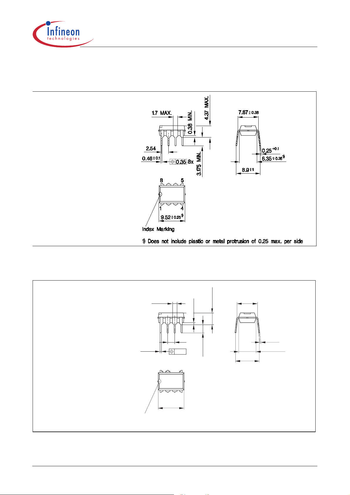
5 Outline Dimension
PG-DIP-8-6
(Plastic Dual In-Line Outline)
CoolSET™-F3
Outline Dimension
Figure 21 PG-DIP-8-6 (Pb-free lead plating Plastic Dual In-Line Outline)
PG-DIP-7-1
(Plastic Dual In-Line Outline)
1.7 MAX.
4.37 MAX.
0.38 MIN.
2.54
±0.1
0.46
Index Marking
1)
Does not include plastic or metal protrusion of 0.25 max. per side
7
1
9.52
0.35
±0.25
7x
3.25 MIN.
5
4
1)
7.87
8.9
±0.38
±1
Figure 22 PG-DIP-7-1 (Pb-free lead plating Plastic Dual In-Line Outline)
0.25
6.35
+0.1
±0.25
1)
Dimensions in mm
Version 2.0 29 24 Aug 2005
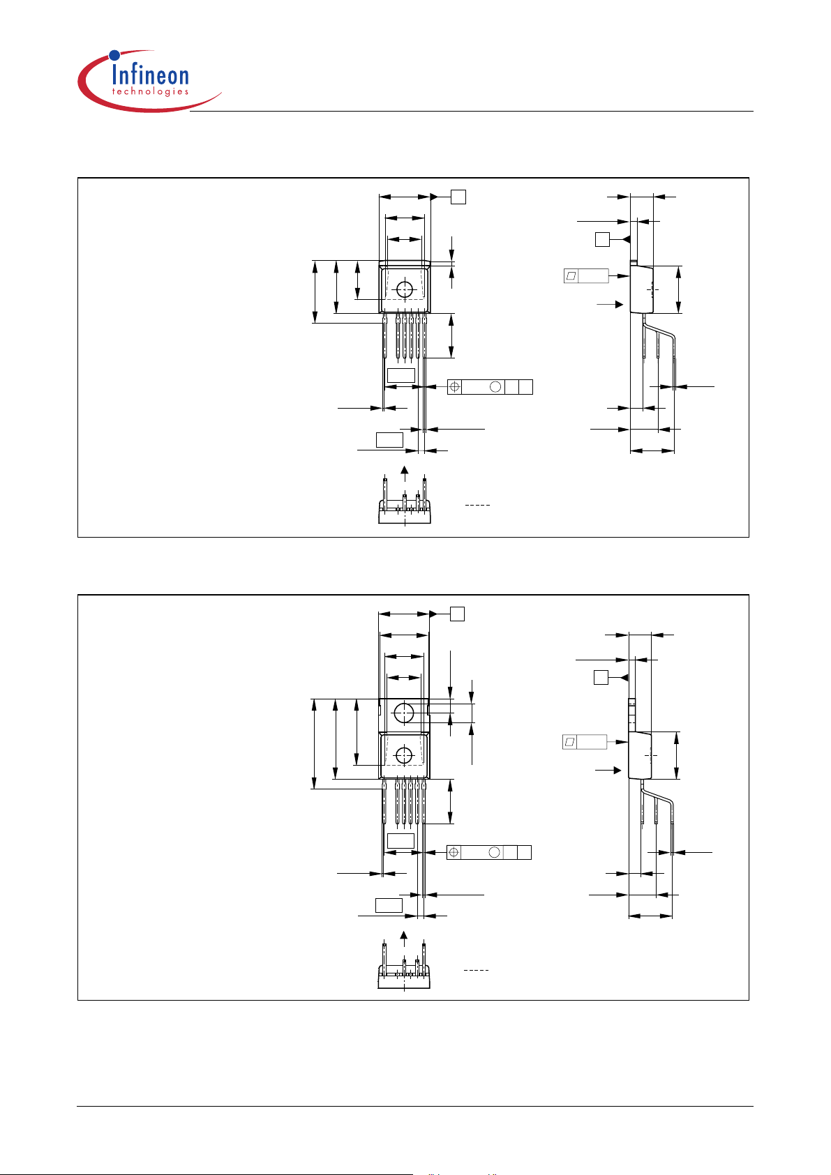
CoolSET™-F3
4.4
9.9
12.1
e
t.
t.
e
9.9
17.5
Outline Dimension
PG-TO220-6-46
(Isodrain I2Pak Package)
7.5
A
1.3
+0.1
-0.02
6.6
(0.8)
±0.3
±0.3
8
0.05
10.2
±0.3
8.6
7.62
0.25 AMB
0...0.15
±0.1
6 x 0.6
5.3
4 x 1.27
1) Shear and punch direction no burrs this surfac
Back side, heatsink contour
All metal surfaces tin plated, except area of cu
Figure 23 PG-TO220-6-46 (Pb-free lead plating Isodrain I2Pak Package)
B
1)
±0.2
9.2
0.5
±0.1
2.4
±0.3
±0.3
8.4
PG-TO220-6-47
(Isodrain Package)
±0.3
±0.3
13
15.6
0...0.15
1.274 x
9.5
7.5
6.6
7.62
±0.2
±0.2
A
±0.2
2.8
±0.3
8.6
6 x 0.6
4.4
+0.1
1.3
-0.02
B
-0.15
3.7
0.25 AMB
0.05
1)
±0.2
9.2
0.5
±0.1
2.4
±0.1
5.3
±0.3
8.4
±0.3
1) Shear and punch direction no burrs this surfac
Back side, heatsink contour
All metal surfaces tin plated, except area of cu
Figure 24 PG-TO220-6-47 (Pb-free lead plating Isodrain Package)
Dimensions in mm
Version 2.0 30 24 Aug 2005

Total Quality Management
Qualität hat für uns eine umfassende
Bedeutung. Wir wollen allen Ihren
Ansprüchen in der bestmöglichen Weise
gerecht werden. Es geht uns also nicht nur
um die Produktqualität – unsere
Anstrengungen gelten gleichermaßen der
Lieferqualität und Logistik, dem Service
und Support sowie allen sonstigen
Beratungs- und Betreuungsleistungen.
Dazu gehört eine bestimmte Geisteshaltung
unserer Mitarbeiter. Total Quality im
Denken und Handeln gegenüber Kollegen,
Lieferanten und Ihnen, unserem Kunden.
Unsere Leitlinie ist jede Aufgabe mit „Null
Fehlern“ zu lösen – in offener Sichtweise
auch über den eigenen Arbeitsplatz hinaus –
und uns ständig zu verbessern.
Unternehmensweit orientieren wir uns
dabei auch an „top“ (Time Optimized
Processes), um Ihnen durch größere
Schnelligkeit den entscheidenden
Wettbewerbsvorsprung zu verschaffen.
quality. We direct our efforts equally at
quality of supply and logistics, service and
support, as well as all the other ways in
which we advise and attend to you.
Part of this is the very special attitude of our
staff. Total Quality in thought and deed,
towards co-workers, suppliers and you, our
customer. Our guideline is “do everything
with zero defects”, in an open manner that is
demonstrated beyond your immediate
workplace, and to constantly improve.
Throughout the corporation we also think in
terms of Time Optimized Processes (top),
greater speed on our part to give you that
decisive competitive edge.
Give us the chance to prove the best of
performance through the best of quality –
you will be convinced.
Geben Sie uns die Chance, hohe Leistung
durch umfassende Qualität zu beweisen.
Wir werden Sie überzeugen.
Quality takes on an allencompassing
significance at Semiconductor Group. For
us it means living up to each and every one
of your demands in the best possible way.
So we are not only concerned with product
http://www.infineon.com
Published by Infineon Technologies AG
 Loading...