

Page 1

Application Note, V1.0, July 2011
Design Guide for LLC Converter
with ICE2HS01G
Power Management & Supply
Never stop thinking.
Page 2

Edition 2011-07-06
Published by Infineon Technologies Asia Pacific,
168 Kallang Way,
349253 Singapore, Singapore
© Infineon Technologies AP 2010.
All Rights Reserved.
Attention please!
The information herein is given to describe certain components and shall not be considered as a guarantee
of characteristics.
Terms of delivery and rights to technical change reserved.
We hereby disclaim any and all warranties, including but not limited to warranties of non-infringement,
regarding circuits, descriptions and charts stated herein.
Information
For further information on technology, delivery terms and conditions and prices please contact your nearest
Infineon Technologies Office (www.infineon.com).
Warnings
Due to technical requirements components may contain dangerous substances. For information on the types
in question please contact your nearest Infineon Technologies Office.
Infineon Technologies Components may only be used in life-support devices or systems with the express
written approval of Infineon Technologies, if a failure of such components can reasonably be expected to
cause the failure of that life-support device or system, or to affect the safety or effectiveness of that device or
system. Life support devices or systems are intended to be implanted in the human body, or to support
and/or maintain and sustain and/or protect human life. If they fail, it is reasonable to assume that the health
of the user or other persons may be endangered.
Page 3

Design Guide for LLC Converter with ICE2HS01
Revision History: 2011-07 V1.0
Previous Version: NA
Design Guide for LLC Converter with ICE2HS01G
License to Infineon Technologies Asia Pacific Pte Ltd A N - P S 0057
Liu Jianwei
Li Dong
Page 4

Page
Table of Content
Abstract ............................................................................................. 5
1
2 Design Procedure ............................................................................ 5
2.1 Target Specifications .................................................................................................................... 5
2.2 Design of Power Stage ................................................................................................................. 6
2.2.1 System specifications ...................................................................................................................... 6
2.2.2 Selection of resonant factor m ........................................................................................................ 6
2.2.3 Voltage gain .................................................................................................................................... 7
2.2.4 Transformer turns ratio .................................................................................................................... 7
2.2.5 Effective load resistance ................................................................................................................. 7
2.2.6 Resonant network ........................................................................................................................... 7
2.2.7 Transformer design ......................................................................................................................... 9
2.2.8 SR MOSFET ................................................................................................................................. 10
2.3 Design of Control Parameters and Protections ....................................................................... 10
2.3.1 Frequency setting: ......................................................................................................................... 10
2.3.2 Minimum/Maximum frequency setting: ......................................................................................... 10
2.3.3 Frequency setting for OCP: ........................................................................................................... 11
2.3.4 Dead time ...................................................................................................................................... 12
2.3.5 Softstart time, OLP blanking time and auto-restart time ............................................................... 13
2.3.6 Load pin setting ............................................................................................................................. 13
2.3.7 Current sense ................................................................................................................................ 13
2.3.8 VINS pin setting ............................................................................................................................ 15
2.3.9 Latch off function and burst mode selection ................................................................................. 15
2.4 Design of Synchronous Rectification (SR) control ................................................................. 16
2.4.1 On-time control - SRD pin and CL pin .......................................................................................... 18
2.4.2 Turn-on delay
- Vres pin ................................................................................................. 20
delayonT_
2.4.3 Advanced Turn off delay
2.4.4 A review of the control scheme ..................................................................................................... 21
2.4.5 SR Protections .............................................................................................................................. 22
2.5 Design summary ......................................................................................................................... 22
- Delay pin .............................................................................. 21
delayoffT_
3 Tips on PCB layout ........................................................................ 24
3.1 Star connection for Power stage ............................................................................................... 24
3.2 Star connection for IC ................................................................................................................. 25
Application Note 4 2011-07-06
Page 5
1 Abstract
ICE2HS01G is our 2nd generation half-bridge LLC controller designed especially for high efficiency with its
synchronous rectification (SR) control for the secondary side. With its new driving techniques, SR can be
realized for half-bridge LLC converter operated with secondary switching current in both CCM and DCM
conditions. No individual SR controller IC is needed at the secondary side.
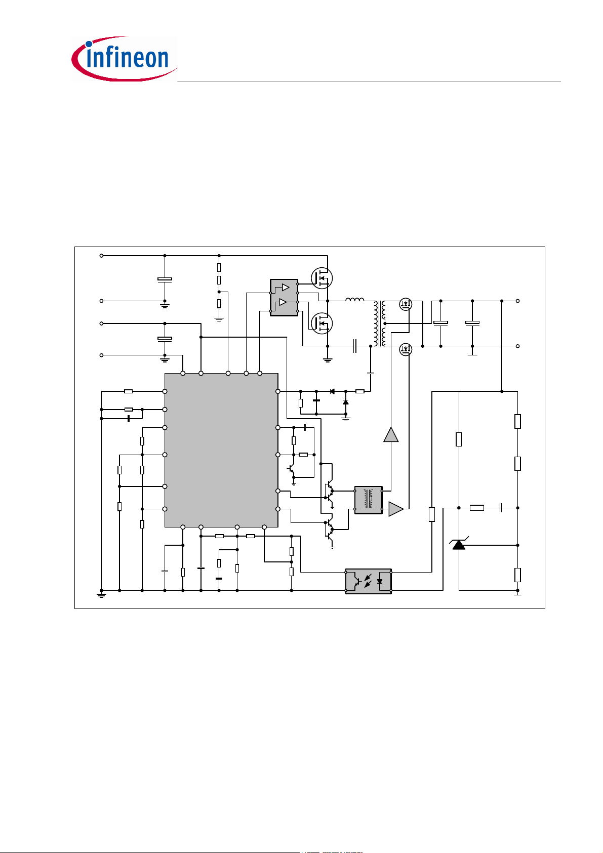
A typical application circuit of ICE2HS01G is shown in Figure 1. For best performance, it is suggested to use
half-bridge driver IC in the primary side with ICE2HS01G.
R
HV
VCC
C
BUS
INS1
R
INS2
R
INS3
HV IC
C
VCC
Q
PH
L
res
Q
PL
C
RES
Q
SH
CO1C
O2
Q
SL
V
out
C
HG LG
R
delay
R
EnA
C
EnA
R
TD
R
R
mc1
R
mc2
GND
Delay
EnA
TD
ICE2HS01G
V
ref
res1
V
mc
V
res
R
res2
C
T
C
R
T
VINSVCC
CS
CL
SRD
SHG
SLG
LOADFREQSSTimer
R
R
SS1
SS
C
SS1
OCP
R
reg
R
FMIN
R
R
CL
Q
SRD
R
FT1
R
FT2
CS2CCS2
C
CL
R
SRD
D
CS1
R
CS1
CS1
D
CS2
R
OVS1
R
IC Driver
Pulse
Trans.
Q
S1
Q
S2
R
Q
S3
Q
S4
IC Driver
OPTO
BA1
BA2
TL431
R
OVS2
C
oc
R
oc
R
OVS3
Figure 1 Typical application circuit
In this application note, the design procedure for LLC resonant converter with ICE2HS01 is presented,
together with an example of a 300W converter with 400VDC. Detailed calculation of the values of the
components around the IC is also included, together with tips on the PCB layout.
2 Design Procedure
2.1 Target Specifications
Application Note 5 2011-07-06
Page 6

The design example is based on the typical application circuit in Figure 1, where individual resonant
choke is implemented. The target specifications are summarized in Table 1.
Input voltage
Output voltage and current
Output power
Efficiency η
Resonant frequency
Hold up time
Bulk capacitor
Table 1 Target application specifications
V
in
P
T
h
C
IV ,
oo
in
f
r
out
2.2 Design of Power Stage
400VDC
12VDC, 25A
~ 300W
>96% at 100% load
>97% at 50% load
>96% at 20% load
85kHz
20ms
270uF
2.2.1 System specifications
The maximum input power can be calculated as:
P
in
Based on the required 20ms hold-up time, the minimum input voltage can be given as:
*
IV
OO
η
VV
25*12
===
96.0
2
2
_min_
nominin
C
out
W
5.312
3
TP
hin
400
2
10*270
−
10*20*5.312*2
6
−
=−=−=
V
2.337
[1]
[2]
2.2.2 Selection of resonant factor m
L
In order to achieve the highest efficiency possible, the value of resonant factor
be set as big as possible, so that the magnetizing inductance
is small, which results in low core loss and conduction loss. On the other hand, the magnetizing current
should be big enough to discharge the
ZVS to ensure safe switching and save switching loss. In this design example,
start. The ZVS of primary side MOSFET will be confirmed later with the determination of the deadtime of
switching.
C of primary side MOSFET during the transitions, to realize
ds
L is big and therefore magnetizing current
m
m
p
== is to
L
r
13=m is selected as a
LL
+
rm
L
r
Application Note 6 2011-07-06
Page 7

=
=
2.2.3 Voltage gain
It is for efficiency optimization to operate the LLC converter around the resonant frequency at nominal
input voltage, where the voltage gain
is neglected due to the implementation of individual resonant choke.
The worst case we need to consider for resonant network and transformer design is the full load
operation at minimum input voltage
M , on condition that the secondary-side leakage inductance
V . The maximum voltage gain at
1
nom
min_in
V can be calculated as:
min_in
V
nomin
_
M [3]
max
V
M
in
nom
min_
400
19.11*
===
2.337
2.2.4 Transformer turns ratio
Assuming the drain-source voltage drop of secondary-side MOSFET VV
ratio will be:
V
_
=
n [4]
nomin
)(2
+
VV
fo
M
nom
=
400
5.161*
=
)1.012(*2
+
1.0
f
, the transformer turns
2.2.5 Effective load resistance
The effective load resistance can be given as:
V
2
eff
nR
2
88
o
I
2
ππ
o
12
2
*5.16*
Ω=== 106
[5]
25
2.2.6 Resonant network
L
Q =
r
C
r
R
eff
f
Defining the normalised frequency to
the voltage gain of the converter can be written as:
2
),(
=
QFMj
)1(
−
mF
22
F = , the load factor of the LLC converter is
f is
r
−−+−
f
r
[6]
QmFjFmF
)1)(1()1(
,
Its magnitude is:
22
)),(Im()),(Re(),( QFMjQFMjQFG += [7]
The graph of voltage gain
Application Note 7 2011-07-06
G Vs F for different Q can be plotted based on [7] with Mathcad:
Page 8
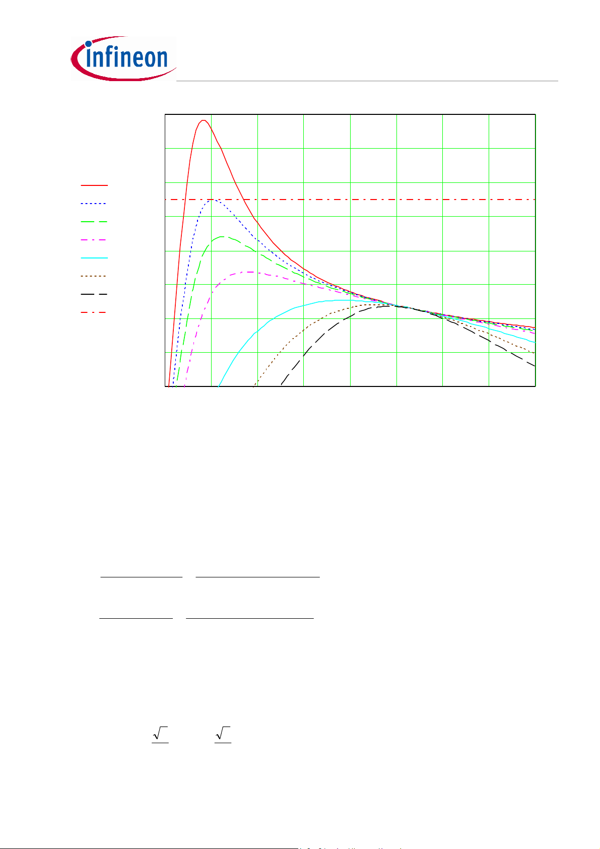
=
=
=
1.5
1.413
GF0.22, ()
GF0.267, ()
GF0.3, ()
GF0.35, ()
GF0.5, ()
GF0.65, ()
GF0.8, ()
Line
Figure 2 Voltage gain G Vs normalized frequency F
Among the curves, we find that the one with
1.325
1.238
1.15
1.063
0.975
0.888
0.8
0.2 0.35 0.5 0.65 0.8 0.95 1.1 1.25 1.4
Q can achieve the required peak gainpkG , which
267.0
F
is 8% higher than
pk
From the curve, the corresponding
Having found the proper
C
r
π
L
r
rp
M for design margin, i.e.
max
28.108.1
== MG
max
F can be located where 28.1
Q, we can calculate the
1
RfQ
***2
effr
π
1
Cf
*)*2(
uHmLL
690==
ππ
rr
min
35.0
C
L
,
and
r
nF
66
===
uH
53
L as follows:
r
1
3
106*10*85*268.0*2
1
===
9232
−
10*66*)10*85*2(
G is achieved.
p
[8]
[9]
2.2.6.1 Resonant choke design
The minimum rms voltage across the resonant network is:
inrmsin
min_min__
Then the corresponding rms current flowing through the resonant choke
22
===
VVV
79.1512.337*
ππ
pk
L
can be calculated as:
r
[10]
Application Note 8 2011-07-06
Page 9

=
+
=
=
Δ
I
rmsin
max__
The peak current is
η
__
P
in
V
*
rmsin
min__
AII
49.3*2.1
==
pkrpkocp
__
300
rmsrpkr
A
06.2
===
[11]
79.151*96.0
AII
91.2*2
==
. The OCP level is set with about 20% margin:
The actual leakage inductance (
shorted is around 13uH. Therefore, the inductance for the independent resonant choke is:
If a magnetic core with specs of RM10/PC95 is selected, where
to be 0.08T to reduce core loss, the minimum turns can be given as:
N
=
min
L
=−=
leakrchoker40_
IL
⋅
__
AB
⋅
minmax
LL
L ) measured at primary side with one of the secondary side winding
leak
uHLLL
90mmA
= , and
min_
e
6
−
pkrchoker
49.3*10*40
6
−
10*90*08.0
4.19
==
2
2.2.7 Transformer design
From Figure 2, the normalized frequency
. Accordingly the actual minimum frequency
pk
min
28.1=
3
kHzfFf
3010*85*35.0*
r
1
= . According to Faraday’s law:
t
2
f
min
===
G
The voltage across the primary winding can be calculated as
period is around:
F
min
35.0
has been located to achieve maximum gain
f is:
min
)(
VVnV
. The half switching cycle
fop
B
max
is selected
[12]
+
)(
VVn
fo
f
2
min
The minimum number of turns at primary side can be found:
N
Where
Then
N
The number of turns at primary side is selected as
calculated accordingly:
Application Note 9 2011-07-06
=
min
p
min
161mmAe= with PQ3230 core. TB 62.0
N can be calculated as:
minp
=
min
p
BAN
Δ=
ep
+
)(
VVn
fo
[13]
BAf
Δ
*2
e
2
)1.012(*5.16
+
63
−
62.0*10*161*10*30*2
33
=
is selected to avoid magnetic saturation.
N . The secondary side turns can be
33
min=p
Page 10

π
N
p
N
s
2.2.8 SR MOSFET
The voltage stress on the drain-source of the MOSFET is:
The RMS value of the current flowing through each MOSFET is:
_
2.3 Design of Control Parameters and Protections
2.3.1 Frequency setting:
2==
n
VVVV
fods
==
ormsd
4
2.242*)( =+=
AII
63.19
The IC internal circuit provides a regulated 2V voltage at FREQ pin. The effective resistance presented
between the FREQ pin and GND, determines the current flowing out of the FREQ pin, which in turn
defines the switching frequency.
Figure 3 shows the curve illustrating the relationship of Switching Frequency
Resistor
R connected between the FREQ pin and gound.
FREQ
FREQ Vs Effective
Figure 3
FREQ
Vs Effective Resistor
R
FREQ
2.3.2 Minimum/Maximum frequency setting:
Application Note 10 2011-07-06
Page 11

=
As discussed in section 2.2.7, the lowest switching
section, how the
Based on the definition of oscillator as in the datasheet and the external circuit around pin FREQ in
Figure 1, the minimum switching frequency will be achieved when pin SS is 2V (usually after softstart),
opto-coupler transistor is open and only
corresponding
for
R .
minF
The maximum operation frequency can possibly be seen when maximum input voltage, say 425V, is
applied, and the converter run in no load condition (
condition can be given as:
f
is actually set by the IC is explained.
min
R is connected to pin FREQ. For kHzf 30
R found from Figure 3 is 50kΩ. A standard value resistor of 51kΩ is selected
FREQ
f will be seen in full load operation at
min
minF
0
Q ), if burst mode is disabled. The gain in this
V . In this
= , the
min
min_in
V
_
nomin
max_
in
+−
max
RRR
//=
M
2
mF
2
−
mF
1
mMm
regeq
M [14]
min
V
From the gain equation, we get:
The corresponding normalized frequency
F
),(
= QM
QFG [15]
=
1
Therefore
For 180 kHz switching frequency, the corresponding equivalent resistance
according to Figure 3. Under no load normal operation, pin SS is already 2V after soft start, and collector
of opto-coupler transistor is pulled to ground, therefore
FMIN
The
R is calculated to be 8.8kΩ. A standard value resistor of 8.2kΩ is selected for the actual design.
reg
nom
−
min
400
94.01*
===
425
)1(
)1(
min
13.2
=
== .
)0(,
==
F can be found by:
max
kHzkHzFf 18085*
R at FREQ pin is 7.5kΩ
eq
2.3.3 Frequency setting for OCP:
Assuming the maximum rms current during over-current should be limited by the IC to 1.2 times the
maximum normal operation, i.e.
The corresponding impedance of the resonant network during over-current can be estimated as:
Z
During over-current, the load impedence is considered to be shorted, and thereofore the impedance of
the resonant network can be calculated as:
Application Note 11 2011-07-06
ocp
V
I
ocp
rmsinrmsocp
max___
rmsin
_
π
*2*
π
2*400
47.2*
LfjZ
rocpocp
π
===
Ω=== 73
1
Cfj
*2*
AII
47.206.2*2.12.1
[16]
π
rocp
−=+=
rocp
Lf
*2
1
Cf
*2
π
rocp
[17]
Page 12

kHzf
Solve the equation and find
R is 5kΩ according to Figure 3. According to the definition of over-current protection,
Then
Then
eq
RRR
//= ,
FMIN
R can be found as 5.6kΩ.
ocp
ocpeq
2.3.4 Dead time
The dead time selection should ensure ZVS of two primary-side MOSFET IPA60R199CP at maximum
switching frequency, where the magnetizing current to charge and discharge
magnetizing current at the end of each switching cycle can be calculated as:
ocp
250=
C is the minimum. The
ds
I
The required time to charge and discharge the
T
Then
=
min
mag
DEAD
R is around 270kΩ according to Figure 4.
TD
+
4
VC
innomds
I
mag
NVV
*)(
edsO
fL
ocpp
=
VC
22
innomds
I
mag
minmin
+
−
5.16*)1.012(
10*250*10*690*4
C is:
ds
12
−
288.0
=
36
400*10*160*2
ns
440
====
[18]
[19]
A
288.0
Figure 4
Application Note 12 2011-07-06
T Vs TDR
DEAD
Page 13

=
=
Ω
=
2.3.5 Softstart time, OLP blanking time and auto-restart time
According to the definition of the softstart of the IC in the datasheet, soft start is implemented by
sweeping the operating frequency from an initial high value until the control loop takes over. The softstart
time depends on a few components, such as the
20ms target rising time of the output voltage, the customer can start with
R , the value of
minF
and the value of
R
ocp
uFC
SS
2.2
.
C . For a
SS
The Timer pin is used to set the blanking time
RC parallel circuit,
OLP blanking time with
The restart time can be calculated as:
C andTR , are connected to this pin. Based on the definition in the datasheet, the
T
Ω= MRT1 and uFC
V
CRmsT
CRT
TTrestart
1ln(**20
TTOLP
V
TL
V
TH
TH
IR
*
BLT
T and restart time
OLP
1
T
66
−
can be calculated as:
525.0
ln(*10*10)ln(**
4
T for over load protection. The
restart
66
−
=−=−=
1ln(*10*10*100020)
ms
20301000*)
4
66
−
10*20*10
ms
240)
=−−=−−=
2.3.6 Load pin setting
One of the functions of the LOAD pin is to detect the over-load or open-loop faults. Once the voltage at this pin
is higher than 1.8V, IC will start internal and external timer and determine the entering of protection mode. The
resistor divider
bottom resistor
regulation.
overload happens. The reference voltage at frequency pin is 2V. Then the voltage at LOAD pin
V
We can find Ω= MR
pin.
= [20]
LOAD
R and
R connected to GND pin should be far bigger than the
As an example, assuming
R
FT
2
RR
+
FT
1
R should be designed properly to ensure OLP is functional as required. The
1FT
2FT
FTFT
21
2FT
MR
FT22
V
82.12*
=
2.0
. A small capacitor of 1nF is usually connected to decouple noise at LOAD
, the target voltage at Load pin is 1.82V when
R , in order not to affect normal
FMIN
2.3.7 Current sense
Application Note 13 2011-07-06
Page 14

π
π
Figure 5 Current sense circuit
Assuming capacitive current divider is adopted as current sense circuit. So
C ,e. g, around 100/rC , say 470pF.
than
200Ω.
r
R is normally of a few hundred Ω for filtering purpose, say
1cs
C is chosen to be far less
1cs
We can obtain the following equation considering
C
cs
= [21]
II
ocpC
cs
1
One major design criterion for the current sense is to ensure Over-Current Protection (OCP). Accordingly,
we can also obtain:
II
RC
where 0.8V is the OCP first level.
1
+
CC
rcs
1
*
==
21
cscs
22
R
C
cs
≈
I
8.0
2
cs
1
ocp
C
r
[22]
C and
1cs
C as current divider:
r
Then we get:
−
R
cs
2
8.0
*2
C
r
*
C
I
ocp
cs
1
8.0
ππ
*
47.2*2
9
10*66
−
12
10*470
[23]
Ω===
70
Rcs2 is chosen as 68Ω.
C is selected so that the current loop speed is fast enough and the ripple on CS pin is around 20% of
2cs
490
f
nF
1
min
.
the average value.
C
2
cs
1
fR
*
min2
cs
CR is around
22*cscs
1
==≈
3
10*30*68
Application Note 14 2011-07-06
Page 15

2.3.8 VINS pin setting
The minimum operation input voltage needs to be specified for LLC resonant converter with the Vins pin.
The typical circuit of mains input voltage sense and process is shown Figure 6.
Figure 6 Mains input voltage sense
The mains input voltage is divided by
connected between VINS and Ground, an adjustable hysteresis between the on and off input voltage can
be created as
Assuming the turn-on bus voltage
typically.The
R
INSH
= k
R
INSL
A standard resistor value for
The blanking time for leaving brown-out is around 500μs and for entering brown-out is around 50μs.
Please note that the calculation above is based on typical specification values of the IC.
=
RIV *=
INSHhyshys
R and
INSH
−
VV
INoffINon
I
INS
RV
INSHth
=
−
VV
thinoff
R can be calculated as:
INSL
=
−
10*10
−
R is 24kΩ.
INSL
R and
INSH
V is 380V typically and the turn-off bus voltage
INon
320380
−
10*6*25.1
M
6
6
6
25.1320
R . With the internal current source
INSL
Ω=
Ω=
5.23
I is
hys
V is 320V
INoff
[24]
[25]
[26]
2.3.9 Latch off function and burst mode selection
Internally, the EnA pin has a pull-up current source of 100μA. By connecting a resistor outside from this
pin to ground, certain voltage level is set up on this pin. If the voltage level on this pin is pulled down
below certain level during operation, IC is latched. If the external resistor has a negative temperature
coefficient, this pin can be used to implement over- temperature protection (OTP). In this design,
selected at 1MΩ to set the pin voltage to be 2V level and no OTP is designed.
Application Note 15 2011-07-06
R is
EnA
Page 16

=
In addition to the latch-off enable function, this pin is also built for the selection of burst mode enable or
not during
LOAD pin voltage falls below 0.12V. However, if burst mode is not selected, the gate drives will not be
stopped by LOAD pin voltage.
The selection block works only after the first time IC VCC increases above UVLO. After CVCC is higher
than turn on threshod, a current source
C . After 26μs, IC will compare the voltage on EnA pin and 1.0V, if voltage on EnA pin is higher than
EnA
1.0V, the burst mode function will be enabled. As the voltage on EnA pin depends on
selecting different capacitance value, whether this IC works with burst mode can be decided.
With
Therefire burst mode will be enabled. If
mode will be disabled.
After the selection is done, the current source
IC starts to sense the EnA pin voltage latch off enable purpose. This blanking time is used to let the EnA
pin votlage be stablized to avoid mistriggering of Latch-off Enable function.
configuration before softstart. If the burst mode is enabled, the gate drives will be disabled if
1 and nFC
EnA
I , in addition to the
sele
Ω= MR
EnAseleEnA
1= , the voltage at EnA pin at the time of 26us can be calculated as:
EnA
6
−
10*26
−
RC
−
C is set to be 10n F, thus burst
EnA
I is turned off. A blanking time of 320μs is given before
66
sele
I , is turned on to charge the capacitor
EnA
R and
EnA
6
−
10*26
−
96
−
10*10
EnA
VVeeRIV
0.156.2)1(*10*10*100)1(*
>=−=−=
usVVV
26@0.126.0 <
C , by
EnA
2.4 Design of Synchronous Rectification (SR) control
Synchronous Rectification (SR) in a half-bridge LLC resonant converter is one of the key factor to achieve
high efficiency. SR control is a major benefit we offer with our new LLC controller IC ICE2HS01G.
Before going into details of SR control of the IC, it’s necessary to understand the ideal SR switching
mechanism for two typical working conditions, i.e. when operation frequency(
and above the resonant frequency (
gate),
V (primary low side gate),
LG
I (current flowing through secondary high side MOSFET),SLI ( current flowing through secondary low
SH
side MOSFET) and
I (current flowing through primary resonant tank).
PRI
f >
f ).Figure 7 illustrates the waveforms of
sw
r
V ( secondary high side gate),
SHG
V (secondary low side gate),
SLG
f ) is below (swf <
sw
V (primary high side
HG
f )
r
Application Note 16 2011-07-06
Page 17

Figure 7 Waveforms for LLC converter with
It can be seen from the waveforms in Figure 7 (left) that to ensure safe switching, the switch-on of the SR
MOSFET (see
while switch-off of the SR MOSFET(see
side switch(see
actual MOSFET. In this operation condition (
depends on the primary gate switching frequency.
From Figure 7 (right), the current flowing through the SR MOSFET (see
switch-off of the primary switch. To avoid the current going into negative, the SR MOSFET need to be
turn off just before the current goes to zero. In this condition, the SR MOSFET on-time is almost constant
and nearly half of the resonant period.
The control of SR in ICE2HS01G consists of four main parts: on-time control, turn-on delay, advanced
turn-off delay and protections, with the block diagram shown in Figure 8.
V ) need to be a certain time AFTER the switch-on of the primary side switch(seeLGV );
SLG
V ) needs to be certain time BEFORE the switch-off of primary
SLG
V ), in order to compensate the propagation delay of the gate signals from IC to the
LG
f >
f (left) and
sw
r
f >
f ), the SR MOSFET conduction period (on-time)
sw
r
f <
f (right)
sw
r
I ) goes to zero before the
SL
Application Note 17 2011-07-06
Page 18

Figure 8 Synchronous rectification control block diagram
2.4.1 On-time control - SRD pin and CL pin
With ICE2HS01’s control scheme, SR MOSFET ‘s turning-off depends on two conditions - turning-off of
the primary gate and the “off” instruction from SR on-time block, where the maximum on-time
preset. Whichever “off” instruction comes first will trigger the turn-off of the SR MOSFET.
As illustrated in the previous chapter, the
converter operates below resonant frequency (
and the SR gate turn-on delay
a safe value as below:
T
on
To achieve higher efficiency, a bigger
MOSFET conduction time and less body diode conduction time, which reduces conduction loss. In actual
design,
switching is guaranteed.
1
f
2
res
T can be fine-tuned by looking at the similar waveforms in Figure 7, as long as safe
max_on
delayonDEAD
_max_
T depends on the resonant frequency when LLC
max_on
f <
f ). Considering the primary side dead time
sw
r
( will be discussed later section 2.4.2), we can preset
delayonT_
usTT
31.525.032.088.5
=−−=−−< [27]
T is an advantage, because bigger on-time means longer SR
max_on
T is
max_on
T
DEAD
T with
max_on
Application Note 18 2011-07-06
Page 19

=
From Figure 9 below,
should start with a smaller SR on time for safety and then adjust it to achieve higher efficiency.
R is selected to be 66kΩ to achieve usT
SRD
31.5
on
max_
. Usually customer
Figure 9 SR on time versus SRD resistance
A simple constant on time control does not provide the best efficiency of LLC HB converter for the whole
load range. In fact, the actual resonant period of secondary current reduces when the output load
decreases or input voltage increases. The primary winding current can reflects this change. The current
sense circuit can be designed to get such information and input to CS pin. In ICE2HS01G, a function
called current level (CL) pin is implemented. During heavy load and low input voltage, the CL pin voltage
(
V ) is clamped at same voltage of SRD pin, 2V. Therefore, the SR on time in such conditions is
CL
determined by
V is reduced to be lower than 2V and extra current will be drawn from SRD pin, thereby the actual SR
CL
on time is reduced. The relationship between
R only and is equal to
SRD
T . In case of light load, with low CS voltage(CSV ), the
max_on
V and CLV is shown in Figure 10(top). The resistorCLR
CS
can be adjusted to find the suitable reducing speed of SR on time for either better reliability or better
efficiency.
calculation for the 300W design example:
We obtain the
V
cs
The corresponding
R is normally around 10 times
CL
R , which is 680kΩ in this design. Below is the detailed
SRD
V for full load condition, based on the circuit in Figure 5:
CS
12
*2
IR
rmsincs
V is clamped at 2V according to Figure 10(top) and the SR on time is
CL
C
max__2
1
cs
*
C
r
06.2*68*2
*
ππ
−
10*470
===
9
−
10*66
V
635.0
T .
max_on
Then for
V = 0.4V where CLV is exactly 2V, the corresponding load is 63% of the full load, which is
CS
around 16A output current(Figure 10, bottom).
Application Note 19 2011-07-06
Page 20

=+=
With
V < 0.4V, CLV starts to drop below 2V, extra current is drawn from SRD pin, thereby the actual
CS
SR on time is reduced with the load decreased.
For filter purpose,
C is chosen to be 47nF.
CL
Figure 10 SR on time versus SRD resistance
2.4.2 Turn-on delay
When the input voltage is higher than resonant voltage, the LLC converter secondary switches are
working in CCM condition. Certain recovery time of the SR MOSFET body diode is required depending on
the current to turn-off. For better performance, the other SR MOSFET should be turn on after the
recovery phase. The turn-on delay function is built in ICE2HS01G for such purpose. When the sensed
input voltage at VINS pin is higher than the reference voltage set by Vres pin according to the resonant
voltage, SR turn-on delay is added, i.e, the SR MOSFETs are turn on 250ns after the corresponding
primary MOSFETs are turned on.
- Vres pin
delayonT_
The nominal bus voltage at resonant point is:
VVVnV
+=
The corresponding voltage at VINS pin is 1.59V. To allow the turn-on delay for input voltage above this
resonant point, we can set the voltage divider
select
operation, we can set the voltage at
and
res
res121
2
2.6
fOres
R and
Ω= kR
, and
R can be calculated to be 5.2kΩ. To disable the turn-on delay during normal
2res
V to be 1.07x1.59=1.7V. Accordingly, Ω= kR
res
Ω= kR
.
3.399)1.012(*5.16*2)(*2
R connected at VRES pin accordingly. We
1res
2res
res121
[28]
,
Application Note 20 2011-07-06
Page 21

Ω
=
2.4.3 Advanced Turn off delay
- Delay pin
delayoffT_
Advanced turn-off delay time of the SR MOSFET
, normally is determined by the propagate
delayoffT_
delay and transition time in the actual converter system. The value of
pin. For example, if the delay time required is 220ns, a
33 need to connect at Delay pin
delay
according to the curve below.
can be set by the Delay
delayoffT_
kR
Figure 11 Turn-off delay time versus Rdelay
2.4.4 A review of the control scheme
After all the SR related parameters have been set, such as maximum on-time
delay
for the two conditions when
From the waveforms on the left, the switch-on of the SR MOSFET is
, advanced turn-off delay
delayonT_
f >
sw
f and
r
, simplified typical waveforms can be drawn in Figure 12
delayoffT_
f <
f .
sw
r
after the switch-on of the
delayonT_
primary side switch; while switch-off of the SR MOSFET is in advance with
primary side switch. Under this operation condition, the SR MOSFET’s on-time changes with the primary
side MOSFET gate switching.
From the waveforms on the right, the SR MOSFET on-time is almost constant and equal to
which is independent of the primary side MOSFET turn-off.
In actual operation, the
signal comes first – the turning-off of the primary gate, or the falling edge of
f doesn’t have to be monitored. SR MOSFET will be turned off by whichever
sw
T .
max_on
T , turn-on
max_on
to the switch-off of
delayoffT_
T ,
max_on
Application Note 21 2011-07-06
Page 22

Figure 12 Waveforms for LLC converter with
f >
sw
f (left) and
r
f <
sw
f (right)
r
2.4.5 SR Protections
As the SR control in ICE2HS01G is realized with indirect method, there are some cases that the SR can
not work properly. In this cases, the SR gate drive will be disabled. Once the condition is over, IC will
restart the SR with SRSoftstart.
During softstart, the SR is disabled.When the softstart pin voltage is higher than 1.9V for 20ms, SR will be
enabled with SRSoftstart.
When LOAD pin voltage is lower than 0.2V, IC will disable the SR immediately. If LOAD pin voltage is
higher than 0.7V, IC will resume SR with SRSoftstart.
During over-current protection phase, if the softstart pin voltage is lower than 1.8V, SR will be disabled.
The SR will resume with softstart 10ms after SS pin voltage is higher than 1.9V again.
In over-current protection, if the CS pin voltage is higher than 0.9V, SR is disabled. SR will be enabled
with SRSoftstart after CS pin voltage is lower than 0.6V.
All the above four conditions are built inside the IC. If IC detects such a condition, IC will disable SR and
pull down the voltage on SRD pin to zero.
When the CS voltage suddenly drops from 0.55V to below 0.30V within 1ms, the SR gate is turned off for
1ms, after 1ms, SR operation is enabled again with SRsoftstart.
If some fault conditions are not reflected on the four conditions mentioned above but can be detected
outside with other measures, the SR can also be disabled and enabled with softstart from outside. This is
implemented on SRD pin as well. The internal SRD reference voltage has limited current source
capability. If a transistor QSRD is connected as shown in typical application circuit, the voltage on SRD
pin can be pulled to zero if this transistor is turned on, which will stop the SR. If the SRD voltage is
released and increases above 1.75V, SR is enabled with softstart.
2.5 Design summary
Figure 13 and 14 show the final schematic for the power stage and control circuit for the 300W LLC
converter.
Application Note 22 2011-07-06
Page 23

C103
2n2/Y1
TR100
PQ3230
R114
430R
R115
430R
S_L G
R123
2k2
ZD100
5V1
ZD101
5V1
SGND
R107
1R0
IC300
GNDNCVDD
INB OUT B
UCC27324_1
S_L D
12V
S_HG
OUTAINA
R108
10k
ZD102
9v1
C109
0m47/16V
C115
100p
R117
3k9
+
C116
100n
C120
NC
S_HD
S_HS
C110
0m47/16V
R118
56R
C117
10n
12V
C111
+
+
0m47/16V
S_PGND
R119
11k
R120
3k01
R125
3k6
R102
1R0
C107
0m47/16V
Q103
015N04
NC
C122
100n
R116
560
+
C119
1u
S_HG
S_L G
S_L S
12V
+
23
R103
10k
0m47/16V
C108
12V
+ C121
10u
C114 47n
R124
NC
1
IC101
TL431
Q101
015N04
+
P_VBUS
P_PGND
P_VCC
P_SGND
RT100 5R
+
C104
10u/25V
C100
270uF/450V
C105
100n/25V
+
P_VCC
P_SGND
P_SL G
P_HG
P_HS
P_VCr
P_PL G
P_PGND
C112
100n
P_SHG
P_Vre g
R109
10R
R110
10R
R100
10R
R104
10R
R111
NC
C118
1n0
R112
NC
R101
10k
R105
10k
Q104
BC546
Q105
BC557
4
3
Q100
IPA60R199CP
Q102
IPA60R199CP
Q107
BC546
Q106
BC557
C113
1u0
IC100
SFH617A-3
L100
40uH//RM10
TR101
EE13
1
2
C102
33nF/630V
33nF/630V
D100
1N4148
D101
1N4148
C106
R121
0R
R122
R106
1k0
R113
1k0
820
Figure 13 Power stage circuit of the half-bridge LLC converter
J?
CON16R
R213
1M0
C209
1u
P_VBUS
1
P_GND
2
P_VCC
3
P_LS
4
NC
5
P_LG
6
P_Vreg
7
Reg GND
8
P_HS
9
P_HG
10
NC
11
P_VCr
12
NC
13
NC
14
P_SLG
15
P_SHG
16
P_Vreg
R205
0M2
C203
820p
R214
1M0
C210
1n0
R215
2M0
C211
2.2u
R207 8k2/1%
R206 5k6/1%
C212
NC
R216
51k/1%
R202
10R
C205
100n
P_VCC
R221
R222
12k
6k2
IC200
HINVCC LIN
GND
IC-ST-L6385
EnA
SS
LOAD
FREQ
Delay
TDCSSRD
Vref
Vres VINS
P_VBUS
IC201
R223
1M5/1%
R224
1M5/1%
R203
11k
R200
10R
R201
11k
C204
100n
R208
261k
NC
R219
0R
R220
R218
33k/1%
R217
NC
Figure 14 Control circuit of the half-bridge LLC converter
GND
VCCTi mer
SHG
SLG
C201
P_HG
100n
P_HS
OUT Vboot
P_LG
LVG HVG
P_VCC
C207
R210
680k
100n
R211
154k/1%
C213
10n
C206
47nF
R228
68R
C200
100n
C208
470p/1kV
R212
200R
D201
1N4148
1N4148
C214
470n
P_VCr
D202
HG
LG
CLVmc
R225
1M5/1%
R226
1M5/1%
P_SHG
P_SLG
R209
154k/1%
R227
24k
Application Note 23 2011-07-06
Page 24

3 Tips on PCB layout
In order to avoid crosstalk on the board between power and signal path, and to keep the IC GND pin as
“clean” from noise as possible, the PCB layout must be taken care of properly. Below are some
suggestions as reference and customer can modify based on their own experience.
3.1 Star connection for Power stage
1. Connect IC VCC Ecap ground to both buck cap. ground and IC VCC ground (please refer to
the red curves in the circuit diagram below)
2. Connect driver IC input ground to IC VCC Ecap ground
3. Connect driver IC output ground to low side MOS source with short path
4. A 100nF filtering cap should be located just near IC VCC & IC GND (refer to the purple arrow)
5. The 100nF filtering cap ground should be inserted between VCC Ecap ground and IC ground
6. Connect driver IC VCC to VCC Ecap(refer to the green curve)
7. Connect driver IC high side output source to half bridge midpoint directly with short path
8. A 100nF filtering cap should be located just near driver IC VCC and IC GND(refer to the blue
arrow)
shorted
Figure 15 PCB layout tips
Application Note 24 2011-07-06
Page 25

3.2 Star connection for IC
1. Connect the following ground directly back to Vcc 100nF cap ground (please refer to the red
curves in the circuit diagram below)
• FREQ pin resistor ground
• Delay pin resistor ground
• SRD resistor ground
R
2. Connetc the following ground with
• SS cap ground
• Opto-coupler ground
3. Connect SR pulse transformer and driving circuit ground to VCC Ecap ground(refer to the yellow
curve)
4. Put 100nF ceramic cap to driver supply (refer to the blue arrow)
5. Connect all other ground using ground plane or ground track back to IC VCC 100nF cap ground
or VCC E cap ground
ground(refer to the green curves)
minF
shorted
Figure 16 PCB layout tips
Application Note 25 2011-07-06
Page 26

References
[1] Infineon Technologies: ICE2HS01 - High Performance Resonant Mode Controller for Half-bridge
LLC Resonant Converter; datasheet Ver 2.0; Infineon Technologies; Munich; Germany; May. 2010.
Application Note 26 2011-07-06
 Loading...