


现货库存、技术资料、百科信息、热点资讯,精彩尽在鼎好!
Datasheet, Version 3.0, September 2001
CoolSET™-F2
ICE2A165/265/365
ICE2A180/280
Off-Line SMPS Current Mode
Controller with integrated 650V/
800V CoolMOS™
Power Management & Supply
Never stop thinking.

CoolSET™-F2
Revision History: 2001-09-19 Datasheet
Previous Version: First One
Page Subjects (major changes since last revision)
For questions on technology, delivery and prices please contact the Infineon Technologies Offices in Germany or
the Infineon Technologies Companies and Representatives worldwide: see our webpage at http://
www.infineon.com
CoolMOS™, CoolSET™ are trademarks of Infineon Technologies AG.
We Listen to Your Comments
Any information within th is document that you feel is wrong, unclear or missing at all?
Your feedback will help us to continuously improve the quality of this document.
Please send your proposal (inc luding a reference to this document) to :
mcdocu.comments@infineon.com
Edition 2001-09-19
Published by Infineon Technologies AG,
St.-Martin-Strasse 53,
D-81541 München
© Infineon Technologies AG 1999.
All Rights Reserv ed.
Attention please!
The information herein is given to describe certain components and shall not be considered as warranted characteristics.
Terms of delivery and rights to technical change reserved.
We hereby disclaim any and all warranties, including but not limited to warranties of non-infringement, regarding
circuits, descriptions and charts stated herein.
Infineon Technologies is an approved CECC manufacturer.
Information
For further information on technology, delivery terms and conditions and prices please contact your nearest Infineon Technologies Office in Germany or our Infineon Technologies Representatives worldwide (see address list).
Warnings
Due to technical requirem ent s components may contain dangerous substances. For information on the types in
question please contact your nearest Infineon Technologies Office.
Infineon Technologies Components may only be used in life-support devices or systems with the express written
approval of Infineon T echnologies, if a failure of such components can reasonably be expected to cause the failure
of that life-support device or system, or to affect the safety or effectiv eness of that device or system. Life support
devices or systems are intended to be implanted in the human body, or to support and/or maintain and sustain
and/or protect human life. If they fail, it is reasonable to assume that the health of the user or other persons may
be endangered.
Off-Line SMPS Current Mode Controller
with integrated 650V/800V CoolMOS™
Product Highlights
• Best of Class in DIP8 Package
• No Heatsink required
• Lowest Standby Power Dissipation
• Enhanced Protection Functions all
with Auto Restart Mode
CoolSET™-F2
ICE2A165/265/365
ICE2A180/280
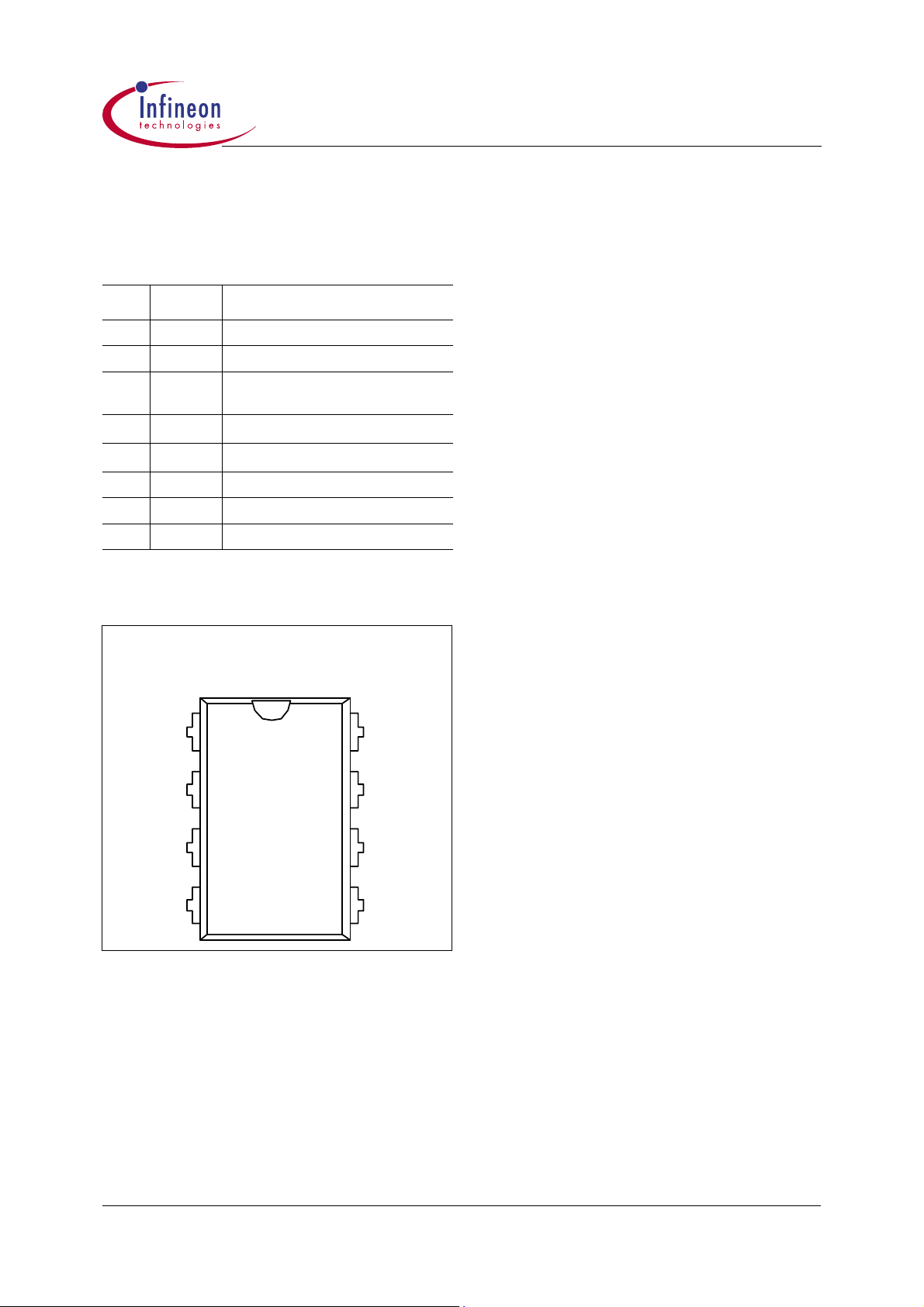
P-DIP-8-6
Features
• 650V/800V Avalanche Rugged CoolMOS™
• Only few external Components required
• Input Undervoltage Lockout
• 100kHz Switching Frequency
• Max Duty Cycle 72%
• Low Power Standby Mode to meet European
Commission Requirements
• Thermal Shut Down with Auto Restart
• Ove r l oad and Open Loop Prot ec tion
• Overvoltage Protection during Auto Rest art
• Adjustable Peak Current Limitation via
External Resistor
• Overall Tolerance of Current Limiting < ±5%
• Internal Leading Edge Blanking
• User defined Soft Start
• Soft Switching for Low EMI
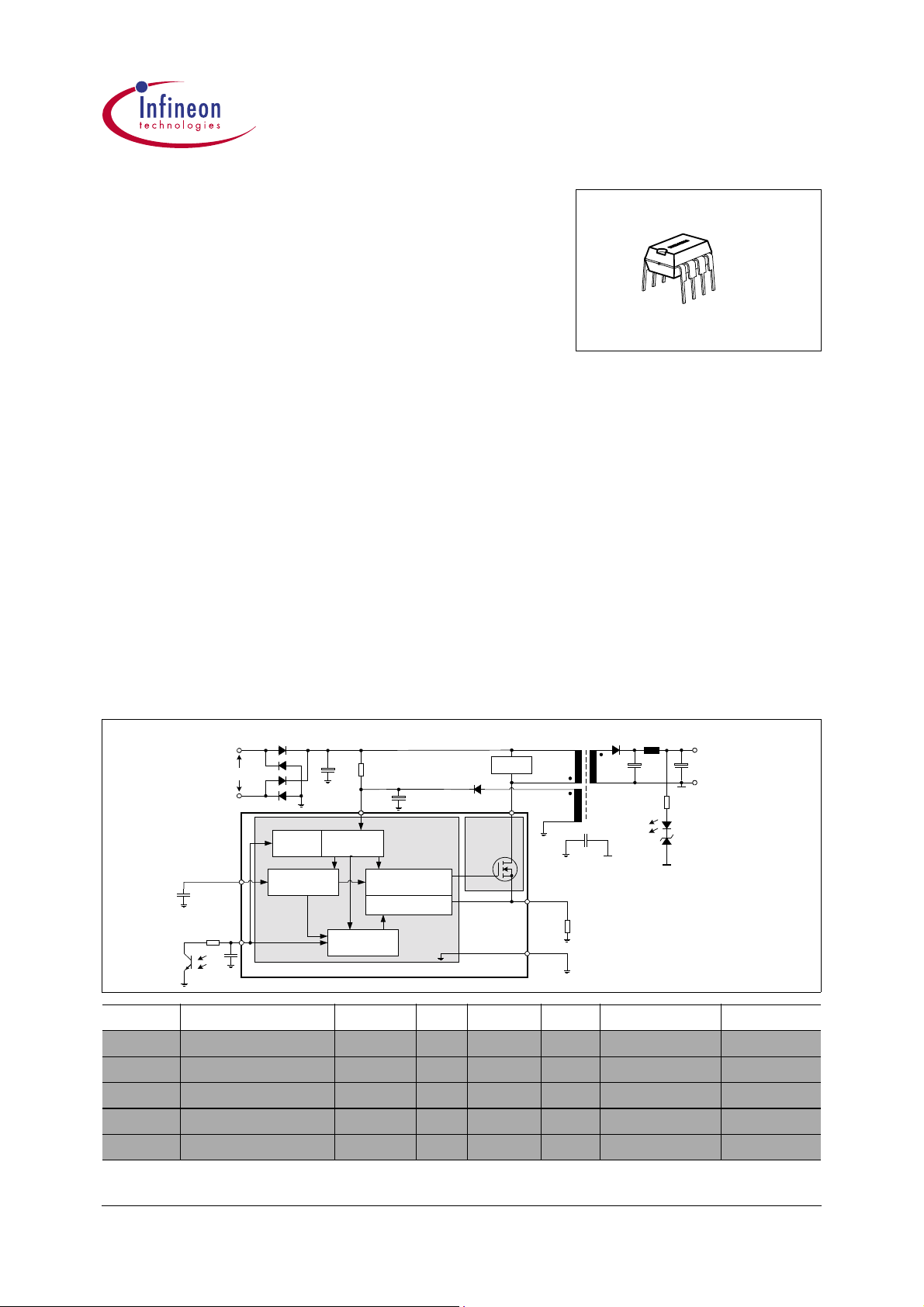
Typical Application
R
VCC
Power
Precise Low Tolerance
Peak Current Limitation
Protection Unit
Start-up
PWM Controller
Current Mode
85 ... 270 VAC
SoftS
C
Soft Start
FB
Feedback
Low Power
StandBy
Soft-Start Control
PWM-Controller
CoolSET™-F2
Management
Description
The second generation CO OLSET™-F2 provides several
special enhancements t o satisfy the needs for low po wer
standby and protection features. In standby mode
frequency reduction is used to lower the power
consumption and support a stable output voltage in this
mode. The frequency reduction is limited to 21.5 kHz to
avoid audible noise. In case of failure modes like open loop,
overvoltage or overload due to short circuit the device
switches in Auto Rest art Mode which is control led by the
internal protection u nit. By means of the internal precise
peak current limitation the dimension of the transformer and
the secondary diode can be lower which leads to more cost
efficiency.
+
Snubber
C
VCC
Drain
CoolMOS™
Isense
GND
Feedback
R
Sense
Converter
DC Output
-
Type Ordering Code Package U
DS
F
OSC
R
DSon
1)
230VAC ±15%
2)
85-265 VAC
2)
ICE2A165 Q67040-S4426 P-DIP-8-6 650V 100kHz 3.0Ω 31W 18W
ICE2A265 Q67040-S4414 P-DIP-8-6 650V 100kHz 0.9Ω 52W 32W
ICE2A365 Q67040-S4415 P-DIP-8-6 650V 100kHz 0.45Ω 67W 45W
ICE2A180 ES Samples available P-DIP-8-6 800V 100kHz 3.0Ω 31W 18W
ICE2A280 Q67040-S4416 P-DIP-8-6 800V 100kHz 0.8Ω 54W 34W
1)
typ @ T=25°C
2)
Maximum power rating at Ta=75°C, Tj=125°C and with copper area on PCB = 6cm²,
Datasheet 3 September 2001

CoolSET™-F2
ICE2A165/265/365
ICE2A180/280
Table of Contents Page
1 Pin Configuration and Functionality . . . . . . . . . . . . . . . . . . . . . . . . . . . . .5
1.1 Pin Configuration . . . . . . . . . . . . . . . . . . . . . . . . . . . . . . . . . . . . . . . . . . . . . .5
1.2 Pin Functionality . . . . . . . . . . . . . . . . . . . . . . . . . . . . . . . . . . . . . . . . . . . . . .5
2 Representative Blockdiagram . . . . . . . . . . . . . . . . . . . . . . . . . . . . . . . . . .6
3 Functional Description . . . . . . . . . . . . . . . . . . . . . . . . . . . . . . . . . . . . . . . .7
3.1 Power Management . . . . . . . . . . . . . . . . . . . . . . . . . . . . . . . . . . . . . . . . . . . .7
3.2 Improved Current Mode . . . . . . . . . . . . . . . . . . . . . . . . . . . . . . . . . . . . . . . . .7
3.2.1 PWM-OP . . . . . . . . . . . . . . . . . . . . . . . . . . . . . . . . . . . . . . . . . . . . . . . . . .8
3.2.2 PWM-Comparator . . . . . . . . . . . . . . . . . . . . . . . . . . . . . . . . . . . . . . . . . . .8
3.3 Soft-Start . . . . . . . . . . . . . . . . . . . . . . . . . . . . . . . . . . . . . . . . . . . . . . . . . . . .9
3.4 Oscillator and Frequency Reduction . . . . . . . . . . . . . . . . . . . . . . . . . . . . . .10
3.4.1 Oscillator . . . . . . . . . . . . . . . . . . . . . . . . . . . . . . . . . . . . . . . . . . . . . . . . .10
3.4.2 Frequency Reduction . . . . . . . . . . . . . . . . . . . . . . . . . . . . . . . . . . . . . . . .10
3.5 Current Limiting . . . . . . . . . . . . . . . . . . . . . . . . . . . . . . . . . . . . . . . . . . . . . .10
3.5.1 Leading Edge Blanking . . . . . . . . . . . . . . . . . . . . . . . . . . . . . . . . . . . . . .10
3.5.2 Propagation Delay Compensation . . . . . . . . . . . . . . . . . . . . . . . . . . . . . .11
3.6 PWM-Latch . . . . . . . . . . . . . . . . . . . . . . . . . . . . . . . . . . . . . . . . . . . . . . . . .11
3.7 Driver . . . . . . . . . . . . . . . . . . . . . . . . . . . . . . . . . . . . . . . . . . . . . . . . . . . . . .11
3.8 Protection Unit (Auto Restart Mode) . . . . . . . . . . . . . . . . . . . . . . . . . . . . . .12
3.8.1 Overload & Open loop with normal load . . . . . . . . . . . . . . . . . . . . . . . . .12
3.8.2 Overvoltage due to open loop with no load . . . . . . . . . . . . . . . . . . . . . . .13
3.8.3 Thermal Shut Down . . . . . . . . . . . . . . . . . . . . . . . . . . . . . . . . . . . . . . . . .13
4 Electrical Characteristics . . . . . . . . . . . . . . . . . . . . . . . . . . . . . . . . . . . . .14
4.1 Absolute Maximum Ratings . . . . . . . . . . . . . . . . . . . . . . . . . . . . . . . . . . . . .14
4.2 Operating Range . . . . . . . . . . . . . . . . . . . . . . . . . . . . . . . . . . . . . . . . . . . . .15
4.3 Characteristics . . . . . . . . . . . . . . . . . . . . . . . . . . . . . . . . . . . . . . . . . . . . . . .15
4.3.1 Supply Section . . . . . . . . . . . . . . . . . . . . . . . . . . . . . . . . . . . . . . . . . . . . .15
4.3.2 Internal Voltage Reference . . . . . . . . . . . . . . . . . . . . . . . . . . . . . . . . . . .15
4.3.3 Control Section . . . . . . . . . . . . . . . . . . . . . . . . . . . . . . . . . . . . . . . . . . . .16
4.3.4 Protection Unit . . . . . . . . . . . . . . . . . . . . . . . . . . . . . . . . . . . . . . . . . . . . .16
4.3.5 Current Limiting . . . . . . . . . . . . . . . . . . . . . . . . . . . . . . . . . . . . . . . . . . . .16
4.3.6 CoolMOS™ Section . . . . . . . . . . . . . . . . . . . . . . . . . . . . . . . . . . . . . . . . .17
5 Typical Performance Characteristics . . . . . . . . . . . . . . . . . . . . . . . . . . .18
6 Outline Dimension . . . . . . . . . . . . . . . . . . . . . . . . . . . . . . . . . . . . . . . . . . .22
Datasheet 4 September 2001
Pin Configuration and Functionality
1 Pin Configuration and Functionality
CoolSET™-F2
ICE2A165/265/365
ICE2A180/280
1.1 Pin Configuration
Pin Symbol Function
1 SoftS Soft-Start
2 FB Feedback
3 Isen s e Controller Current Sense Input,
CoolMOS™ Source Output
4Drain
5Drain
6 N.C Not connected
7 VCC Controller Supply Voltage
8 GND Controller Ground
1)
at Tj = 110°C
2)
at Tj = 110°C
1)
/800V CoolMOS™ Drain
650V
2)
/800V CoolMOS™ Drain
650V
Package P-DIP-8-6
1.2 Pin Functionality
SoftS (Soft Start & Auto Restart Control)
This pin combines the function of Soft Start i n case of
Start Up and Auto Restart Mod e and the con troll ing of
the Auto Restart Mode in case of an error detection.
FB (Feedback)
The information about the regulation is provided by the
FB Pin to the internal Protection Unit and to the internal
PWM-Comparator to control the duty cycle.
Isense (Current Sens e)
The Current Sense pin sense s the voltage develop ed
on the series resistor inserted in the source of the
integrated CoolMOS™. When Isense reaches the
internal threshold of th e Current Limi t Compara tor , the
Driver output is disabled. By this means the Over
Current Detection is realized.
Furthermore the current information is provided for the
PWM-Comparator to realize the Current Mode.
Drain (Drain of integrated CoolMOS™)
Pin Drain is the connection to the Drain of the internal
CoolMOS
TM
.
SoftS
Isense
Drain
Figure 1 Pin Configuration (top view)
1
2
3
4
8
7
6
5
GND
VCCFB
N.C
Drain
VCC (Power supply)
This pin is the positiv su pply of the IC. The opera ting
range is between 8.5V and 21 V.
To provide overvoltage protection the driver gets
disabled when the voltage becomes higher than 16.5V
during Start Up Phase.
GND (Ground)
This pin is the ground of the primary side of the SMPS.
Datasheet 5 September 2001
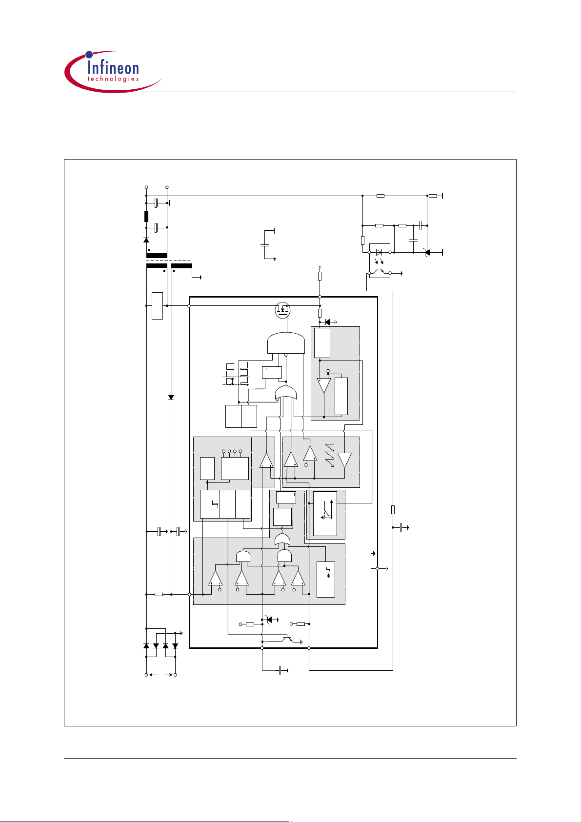
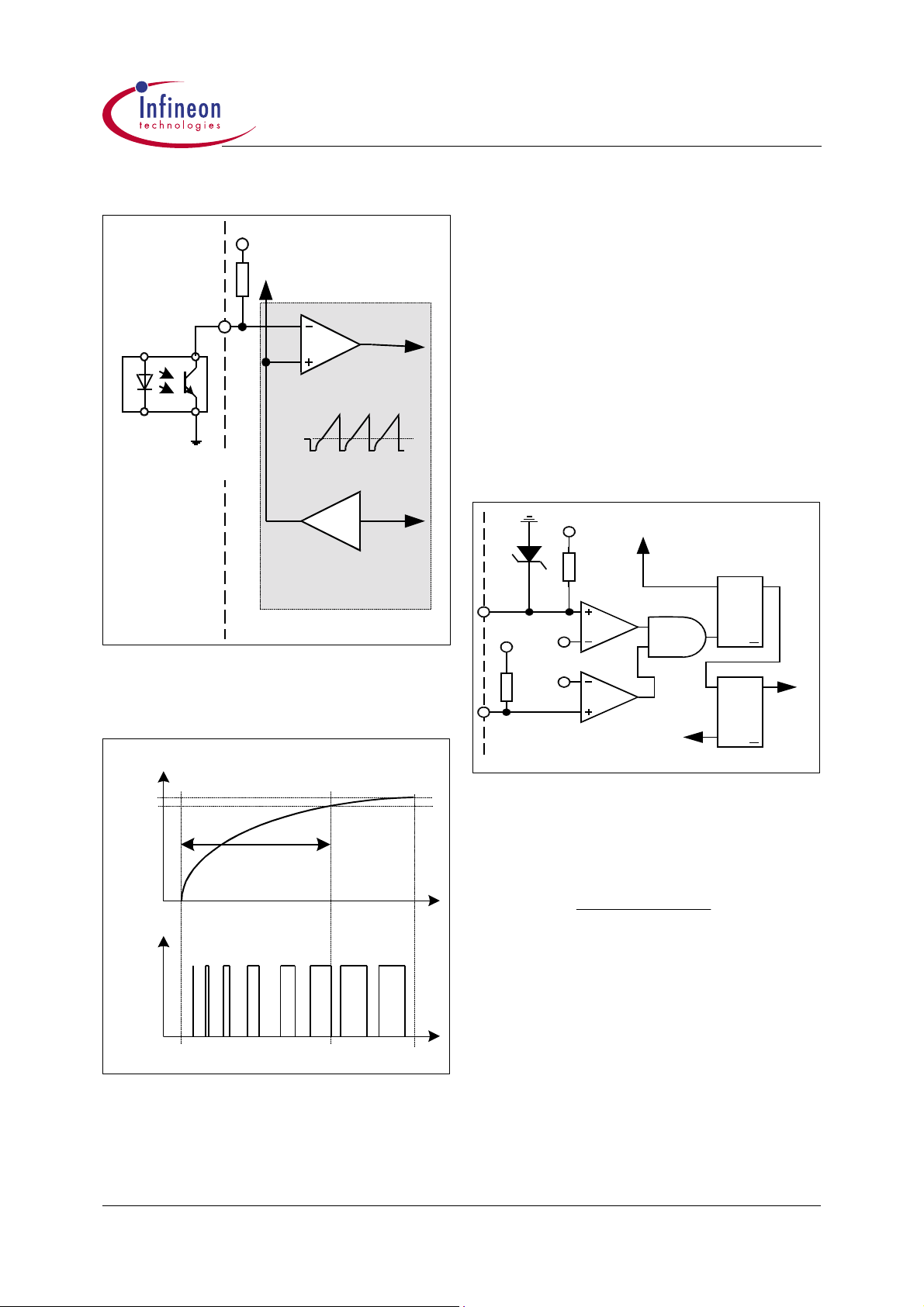
2 Representative Blockdi agram
-
OUT
+
V
Converter
DC Output
Sense
R
Snubber
Drain
Ω
10k
CoolSET™-F2
ICE2A165/265/365
ICE2A180/280
Representative Blockdiagram
Optocoupler
Isense
D1
CoolMOS™
Gate
Driver
Q
Q
S
21.5-100kHz
Soft-Start
R
PWM-Latch
Soft-Start
Comparator
Soft Start
SoftS
5.6V
C
R
Spike
Soft-Start
G4
SQ
Blanking
G3
G2
C4
5.3VC34.8V
PWM
Q
R
s
µ
5
6.5V
T1
0.72
max
Clock
Duty Cycle
Oscillator
6.5V
4.8V
5.3V
4.0V
Bias
Internal
Voltage
Reference
13.5V
Power Management
Line
VCC
C
C
Start-up
R
VCC
Lockout
8.5V
Undervoltage
C1
16.5V
Reset
Power-Down
6.5V
4.0V
Reset
Power-Up
G1
C2
Comparator
0.3V
Error-Latch
FB
R
C5
Blanking
Leading Edge
Comparator
Current-Limit
osc
f
Thermal
FB
200ns
csth
V
0.8V
FB
U
21.5kHz
100kHz
Shutdown
>140°C
j
T
Compensation
Propagation-Delay
x3.65
PWM OP
Standby Unit
Protection Unit
Current Limiting
Improved Current Mode
GND
CoolSET™-F2
85 ... 270 VAC
Figure 2 Represent a tive Blockdia gr a m
Datasheet 6 September 2001
3 Functional Description
CoolSET™-F2
ICE2A165/265/365
ICE2A180/280
Functional Description
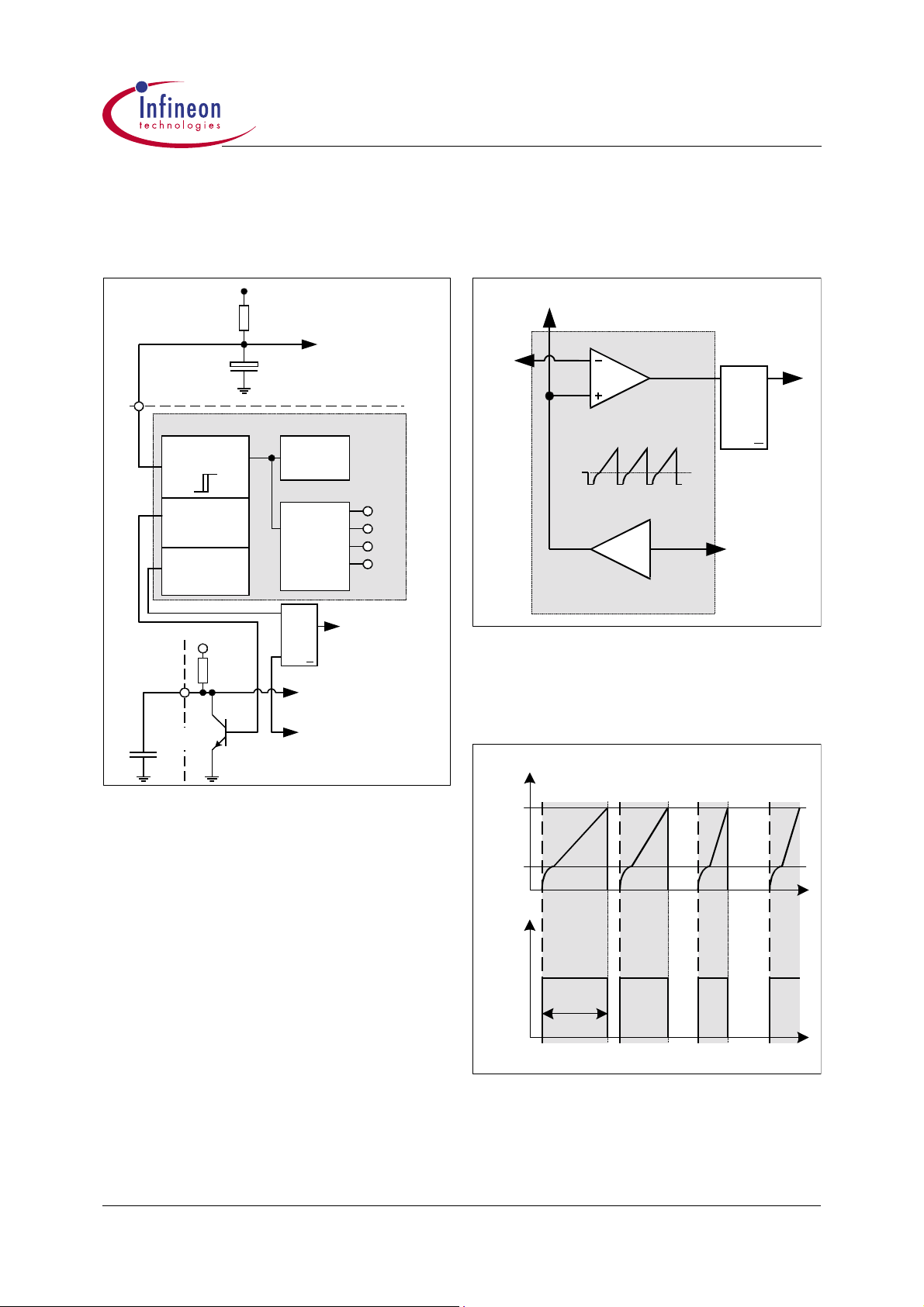
3.1 Power Management
Main Line (100V-380V)
R
Start-Up
C
VCC
VCC
Power Management
So ftS
C
Soft-S ta rt
Undervoltage
Lockout
8.5V
Pow er-D ow n
Reset
Pow er-U p
Reset
T1
13.5V
6.5V
R
Soft-S tart
Internal
Bias
Voltage
Reference
RSQ
Q
Error-Latch
So ft-Start C om para to r
Error-D etec tion
Primary Winding
6.5V
5.3V
4.8V
4.0V
PWM-Latch
3.2 Improved Current M ode
Soft-Start Com parator
FB
PW M-Latch
RSQ
Driver
PW M C om parator
Q
0.8V
PW M O P
x3.65
Isense
Improved
Current Mode
Figure 4 Current Mode
Current Mode means that the d uty cycle is controlled
by the slope of the primary current. This is done by
comparison the FB signal with the amplified current
sense signal.
Figure 3 P ower Management
The Undervoltage Lockout monitors the external
supply voltage V
. In case the IC is inactive the
VCC
current consumption is max. 55µA. When the SMPS is
plugged to the main line the current through R
charges the external Capacitor C
exceeds the on -threshold V
=13.5V the internal bias
CCon
. When V
VCC
Start-up
VCC
circuit and the voltage reference are switched on. After
it the internal ba ndgap generates a refere nce voltage
V
=6.5V to supply the internal circuits. To avoid
REF
uncontrolled ringing at switch-on a hysteresis is
implemented which mea ns that switch-off is only af ter
active mode when Vcc falls below 8.5V.
In case of switch-on a Power Up Reset is done by
reseting the internal error-latch in the protection unit.
When V
falls below the off-threshold V
VCC
CCoff
=8.5V the
internal reference is sw itched off and t he Powe r Dow n
reset let T1 discharging the soft-start capacitor C
Soft-Start
at pin SoftS. Thus it is ensured that at every switch-on
the voltage ramp at pin SoftS starts at zero.
Am plified Current Signal
FB
0.8V
Driver
T
on
t
t
Figure 5 Pulse Width Modula ti on
In case the amplified current sense signal exceeds the
FB signal the on-time T
reseting the PWM-Latch (see Figure 5).
of the driver is finished by
on
Datasheet 7 September 2001

The primary current is sensed by the external series
resistor R
inserted in the source of the inte grated
Sense
CoolMOS™. By means of Current Mode the regulation
of the secondary voltage is insensitive on line
variations. Line variation causes varition of the
increasing current slope which contro ls th e duty cycle.
The external R
allows an individual a djustment of
Sense
the maximum source current of the integrated
CoolMOS™.
S oft-Sta rt Co mp a ra to r
PW M C om parator
FB
PW M-Latch
V
OSC
Duty Cycle
Voltage Ram p
0.8V
FB
0.3V
CoolSET™-F2
ICE2A165/265/365
ICE2A180/280
Functional Description
max.
t
Oscillator
0.3V
C5
V
OSC
G a te Driv e r
0.8V
10k
Ω
x3.65
T
2
C
1
R
1
20pF
V
1
PWM OP
Voltage Ram p
Figure 6 Improve d Current Mode
To improve the Current Mode during light load
conditions the amplified current ramp of the PWM-OP
is superimposed on a voltage ramp , which is built by
the switch T
low pass filter composed of R
Figure 7). Every time the oscillator shuts down for max.
duty cycle limitation the switch T2 is closed by V
When the oscillator triggers the Gate Driver T2 is
opened so that the voltage ramp can start.
In case of light load the amplified current ramp is to
small to ensure a stable regulation. In that case the
Voltage Ramp is a well defined signal for the
comparison with the FB-signal. The duty cycle is then
controlled by the slope of the Voltage Ramp.
By means of the C5 Comparator the Gate Driver is
switched-off until the voltage ramp exceeds 0.3V. It
allows the duty cycle to be reduced continou sly till 0%
by decreasing V
, the voltage source V1 and the 1st order
2
below that threshold.
FB
and C1(see Figure 6,
1
OSC
G a te D r ive r
Figure 7 Light Load Conditions
3.2.1 PWM-OP
The input of the PWM-OP is applied over t he internal
leading edge blanking to the external sense resistor
R
connected to pin ISense. R
Sense
source current into a sense voltage. The sense voltage
is amplified with a gain of 3.65 by PWM OP. The output
of the PWM-OP is connected to the voltage source V1.
The voltage ramp with the superimposed amplified
current singal is fed into the positive inputs of the PWMComparator, C5 and the Soft-Start-Comparator.
.
3.2.2 PWM-Comparator
The PWM-Comparator compares the sensed current
signal of the i ntegrated CoolMOS
signal V
(see Figure 8). VFB is created by an external
FB
optocoupler or external transistor in combination with
the internal pullup re sistor R
and provides the load
FB
information of the feedback circuitry. When the
amplified current signal of the integrated CoolMOS™
exceeds the signal V
the PWM-Compar ator swi tches
FB
off the Gate Driver.
converts the
Sense
TM
with the feedback
t
t
Datasheet 8 September 2001
CoolSET™-F2
ICE2A165/265/365
ICE2A180/280
Functional Description
6.5V
R
FB
S o ft-Sta rt C o mp a ra t o r
FB
PW M C om parator
0.8V
Optocoupler
PW M O P
Figure 8 PWM Controlling
3.3 Soft-Start
V
SoftS
5.6V
5.3V
T
S of t-S ta rt
PWM -Latch
Isense
x3.65
Improved
Current Mode
pullup resistor R
. The Soft-Start-Comparator
Soft-Start
compares the voltage at pin SoftS at the negative input
with the ramp signal of the PWM-OP at the positive
input. When Soft-Start voltage V
Feedback voltage V
the Soft-Start-Comparator limits
FB
is less than
SoftS
the pulse width by reseting the PWM-Latch (see Figure
9). In addition to Start -Up, Soft-Start is a lso activated at
each restart attempt duri ng Aut o Resta rt . By mean s of
the above mentioned C
the Soft-Start can be
Soft-Start
defined by the user. The Soft-Start is finished when
V
exceeds 5.3V. At that ti me the Prot ection Uni t is
SoftS
activated by Comparator C4 and senses the FB by
Comparator C3 wether the voltage is below 4.8V which
means that the voltage on the secondary side of the
SMPS is settled. The internal Zener Diode at SoftS with
breaktrough voltage of 5.6V is to pre vent the internal
circuit from saturation (see Figure 10).
5.6V
SoftS
6.5V
FB
5.3V
4.8V
R
FB
6.5V
R
Power-Up Reset
So ft-Sta rt
C4
C3
Clock
Error-Latch
G2
PW M-Latch
RSQ
Q
RSQ
Gate
Driver
Q
Figure 10 Activation of Protection Unit
The Start-Up time T
voltage V
Start Phase T
is settled must be shorter than the Soft-
OUT
Soft-Start
within the conver ter output
Start-Up
(see Figure 11).
T
−
StartSoft
−
StartSoft
69,1×
Gate Driver
C
t
=
−
StartSoft
R
By means of Soft-Start there is an effective
minimization of current and voltage stresses on the
integrated CoolMOS™, the clamp circuit and the output
overshoot and prevent s saturation of the transforme r
during Start-Up.
t
Figure 9 Soft-Start Phase
The Soft-Start is r e al i z ed by the internal pu ll u p r es i s to r
R
Figure 2). The Soft-Start voltage V
charging the external capacitor C
and the external Capacitor C
Soft-Start
Soft-Start
is generated by
SoftS
by the internal
Soft-Start
(see
Datasheet 9 September 2001

CoolSET™-F2
ICE2A165/265/365
ICE2A180/280
Functional Description
V
SoftS
5.3V
T
So ft-Sta rt
V
FB
4.8V
V
OUT
V
OUT
T
Start-Up
Figure 11 Start Up Phase
3.4 Oscillator and Frequency
Reduction
kHz
100
65
OSC
f
21,5
0,9
t
1,0
1,1 1,2 1,3 1,4 1,5 1,6 1,7 1,8 1,9 2
V
FB
Figure 12 Frequency Dependence
3.5 Current Limiting
There is a cycle by cycle current limiting realised by the
t
Current-Limit Comparator to provide an overcurrent
detection. The source current of the integrated
CoolMOS
R
Sense
transformed to a sense voltage V
voltage V
V
t
csth
off the gate drive. To prevent the Current Limiting from
distortions caused by leading edge spikes a Lead ing
Edge Blanking is integrated at the Current Sense.
Furthermore a Propagation Delay Compensation is
added to support the immedeate shut down of the
CoolMOS™ in case of overcurrent.
TM
is sensed via an external sense resistor
. By means of R
exceeds the internal threshold voltage
Sense
the source current is
Sense
Sense
the Current-Limit-Comparator immediately turns
V
. When the
3.4.1 Oscillator
The oscillator generates a frequency f
resistor, a capacitor and a current source and current
sink which determine the frequency are integrated. The
charging and discharging current of the implemented
oscillator capacitor are intern ally trimmed, in order to
achieve a very accurate switching frequency. The ratio
of controlled charge to discharge current is adjusted to
reach a max. duty cycle limitation of D
= 100kHz. A
switch
=0.72.
max
3.4.2 Frequency Reduction
The frequency of the oscillator is depending on the
voltage at pin FB. The d epe ndence is sho wn in F igu re
12. This feature allows a power supply to op erate at
lower frequency at light loads thus lowering the
switching losses while maintaining good cross
regulation performan ce and low output ripple. In case
of low power the power consumption of the whole
SMPS can now be reduced very effective. The minimal
reachable frequency is limited to 21.5 kHz to avoid
audible noise in any case.
3.5.1 Leading Edge Blanking
V
Sense
V
csth
t
= 220ns
LEB
t
Figure 13 Leading Edge Blanking
Each time when CoolMOS™ is switched on a le ading
spike is generated due to the primary-side
capacitances and secondary-side rectifier reverse
recovery time. To avoid a premature termination of the
switching pulse this spi ke is blanked out with a time
constant of t
the Current-Limit Comparator cannot switch off the
gate drive.
= 220ns. During that time the output of
LEB
Datasheet 10 September 2001

CoolSET™-F2
t
ICE2A165/265/365
ICE2A180/280
Functional Description
3.5.2 Propagation Delay Compensation
In case of overcurrent detection by I
of CoolMOS ™ is delayed due to the propagation delay
of the circuit. This delay causes an over shoot of the
peak current I
which depends on the ratio of dI/dt of
peak
the peak current (see Figure 14).
.
I
Sense
I
peak2
I
peak1
I
Limit
I
Overshoot2
Figure 1 4 Current Limiting
The overshoot of Signal2 is bigger than of Signal1 due
to the steeper rising waveform.
A propagation delay compensation is integrated to
bound the overshoo t dependent on dI/dt of t he rising
primary current. That means the propagation delay
time between exceeding the current sense threshold
V
and the switch off of CoolMOS™ is compensated
csth
over temperature within a range of at least.
dI
R
Sense
dt
peak
10 ≤×≤
So current limiting is now ca pable in a very accurate
way (see Figure 16).
V
OSC
max. Duty Cycle
Limit
Signal1Signal2
t
Propagation Delay
dV
Sense
dt
the shut down
I
Overshoot1
t
The propagation delay compensation is done by
means of a dynamic threshold voltage V
(see Figure
csth
15). In case of a steeper slope the switch off of the
driver is earlier to compensate the de lay.
E.g. I
= 0.5A with R
peak
= 2 . Without pr opagation
Sense
delay compensation the cu rrent sense thresh old is set
to a static voltage level V
dI/dt = 0.4A/µs, that means dV
propagation delay time of i.e. t
leads then to a I
peak
=1V. A current ramp of
csth
/dt = 0.8V/µs, and a
Sense
Propagation Delay
=180ns
overshoot of 12%. By means of
propagation delay compensatio n the overshoo t is only
about 2% (see Figure 16).
with compensation without compensation
V
1,3
1,25
1,2
1,15
Sense
1,1
V
1,05
1
0,95
0,9
0 0,2 0,4 0,6 0,8 1 1,2 1,4 1,6 1,8 2
dV
Sense
d
V
s
µ
Figure 16 Overcurrent Shutdown
3.6 PWM-Latch
The oscillator clock output appl ies a set pulse to the
PWM-Latch when initiating CoolMOS™ conduction.
After setting the PWM-Latch can be reset by the PWMOP, the Soft-Start-Comparator, the Current-LimitComparator, Comparator C3 or the Error-Latch of the
Protection Unit. In case of resetin g the driver is shut
down immediately.
3.7 Driver
off time
V
Sense
V
csth
Propagation Delay
Signal1 Signal2
Figure 15 Dynamic Voltage Threshold V
t
t
csth
The driver-stage drives the gate of the CoolMOS™
and is optimized t o minimize EMI and to provide high
circuit efficiency. This is done by reducing the switch on
slope when reaching the CoolMOS™ threshold. This is
achieved by a slope control of the rising edge at the
driver’s output (see Figure 17).
Thus the leading switch on spike is minimized. When
CoolMOS™ is switched off, the falling shape of the
driver is slowed down when reaching 2V to prevent an
overshoot below ground. Furthermore the driver circuit
is designed to eliminate cross conduct ion of the output
stage. At voltages below the undervoltage lockout
threshold V
the gate drive is active low.
VCCoff
Datasheet 11 September 2001

CoolSET™-F2
ICE2A165/265/365
ICE2A180/280
Functional Description
V
5V
Gate
ca. t = 130ns
t
Figure 17 Gate Rising Slope
3.8 Protection Unit (Auto Re start Mode)
An overload, open loo p and overvoltage detection is
integrated within the Protection Unit. These three
failure modes are latched by an Error-Latch. Additional
thermal shutdown is latched by the Error-Latch. In case
of those failure modes the Error-Latch is set after a
blanking time of 5µs and the C ool MOS™ is shut down.
That blanking pr eve nts the Err or-L atc h fr om di sto rti ons
caused by spikes during operation mode.
3.8.1 Overload & O pen loop wi th normal
load
Figure 18 shows the Auto Restart Mode in case of
overload or open l oop w ith norma l loa d. T he det ectio n
of open loop or overload is provided by the Comparator
C3, C4 and the AND-gate G2 (see Figure19). The
detection is activa ted by C4 when the vol tage at pin
SoftS exceeds 5.3V. Till this time the IC operates in the
Soft-Start Phase. After this phase the comparator C3
can set the Error-Latch in case of open loop or overload
which leads the feedback voltage V
threshold of 4.8V. After latching VCC decreases till
8.5V and inactivates t he IC. At this time the external
Soft-Start capacitor is discharged by the internal
transistor T1 due to Powe r Down Reset. When th e IC
is inactive V
the Capacitor C
R
. Then the Error-Latch is reset by Power Up
Start-Up
increases till V
VCC
by means of the Start-Up Resistor
VCC
CCon
Reset and the external Soft -Start capacitor C
charged by the internal pullup resistor R
the Soft-Start Phase which ends when the voltage at
pin SoftS exceeds 5. 3V the detection of overload an d
open loop by C3 and G2 is inactive. In this way the Start
Up Phase is not detect ed as an overload.
to exceed the
FB
= 13.5V by charging
is
Soft-Start
. During
Soft-Start
O v e r lo a d & O pe n loo p /n o r ma l loa d
5µs Blanking
FB
4.8V
Fa ilu r e
Detection
SoftS
5.3V
Soft-S tart Ph a se
T
Driver
VCC
13.5V
8.5V
Burst1
Figure 18 Auto Restart Mode
So ftS
FB
C
So ft-Sta rt
6.5V
R
T1
Power Up Reset
So ft-Sta rt
C4
5.3V
4.8V
C3
T
Restart
G2
t
t
t
t
Erro r-L atch
R
FB
6.5V
Figure 19 FB-Detection
Datasheet 12 September 2001

CoolSET™-F2
ICE2A165/265/365
ICE2A180/280
Functional Description
But the Soft-Sta rt Phase must be finished within the
Start Up Phase to force the voltage at pin FB below the
failure detection thresh old of 4.8V.
3.8.2 Overvoltage due to open loop with
no load
Open loop & no load condition
5µs Blanking
FB
4.8V
Failure
Detection
So ftS
5.3V
4.0V
Driver
VCC
16.5V
13.5V
Soft-Start Phase
Overvoltage
Detection Phase
T
Overvoltage Detection
Burst2
T
Restart
t
t
t
detection due to varying of VCC concerning the
regulation of the co nverter output. When the voltage
V
is above 4.0V the ov ervoltage detection by C1 is
SoftS
deactivated.
VCC
6.5V
C1
16.5V
R
So ft-S tart
4.0V
SoftS
C
Soft-Start
T1
C2
Power Up Reset
Figure 21 Overvoltage Detection
3.8.3 Thermal Shut Down
Thermal Shut Down is latched by the Error-Latch when
junction temperature T
exceeding an internal thre shold of 1 40°C. In that c ase
the IC switches in Auto Restart Mode.
of the pwm controller is
j
Error Latch
G1
8.5V
t
Figure 20 Auto Restart Mode
Figure 20 shows the Auto Restart Mode for open loop
and no load co nditi on. In case o f this failure mode the
converter output voltage in creases and also VCC. An
additional protect ion by the comparators C1, C2 and
the AND-gate G1 is implemented to consider this
failure mode (see Figure 21).The overvoltage detection
is provided by Comparator C1 only in the first time
during the Soft-Start Phase till the Soft-Start voltage
exceeds the threshold of t he Comparator C2 at 4.0V
and the voltage at pin FB is abo ve 4.8V. When VCC
exceeds 16.5V durin g the ov er volt ag e dete cti on ph ase
C1 can set the E r r or- L atch and the Bu r s t P h as e during
Auto Restart Mode is finished earlier. In that case
T
is shorter than T
Burst2
. By means of C2 the
Soft-Start
normal operation mo de is preven ted from overvoltage
Note: All the values which are mentioned in the
functional descriptio n are typical. Please refer
to Electrical Characteristics for min/max limit
values.
Datasheet 13 September 2001

CoolSET™-F2
ICE2A165/265/365
ICE2A180/280
Electrical Characteristics
4 Electrical Characteristics
4.1 Absolute Maximum Ratings
Note: Absolute maxi mum ratings are defi ned as ratings, which when being exceed ed may lead to destruct ion
of the integrated circuit. For the same reason make sure, that any capacitor that will be connected to pin 6
(VCC) is discharged before a ssembling the application circuit.
Parameter Symbol Limit Values Uni t Remarks
min. max.
Drain Source Voltage
V
DS
-650VT
ICE2A165/265/365
Drain Source Voltage
V
DS
-800V
ICE2A180/280
Avalanche ener gy,
repetitive t
max. T
AR
=150°C
j
limited by
1)
ICE2A165 E
ICE2A265 E
ICE2A365 E
ICE2A180 E
ICE2A280 E
Avalanche curr ent,
repetitive t
max. T
AR
=150°C
j
limited by
1)
ICE2A165 I
ICE2A265 I
ICE2A365 I
ICE2A180 I
ICE2A280 I
Supply Voltage V
V
CC
FB Voltage V
SoftS Voltage V
ISense I
Junction Temperature T
Storage Tempe rature T
Thermal Resistance
AR1
AR2
AR3
AR4
AR5
AR1
AR2
AR3
AR4
AR5
CC
FB
SoftS
Sense
j
S
R
thJA
-0.2mJ
-0.4mJ
-0.5mJ
-0.2mJ
-0.4mJ
-1A
-2A
-3A
-1A
-2A
-0.3 22 V
-0.3 6.5 V
-0.3 6.5 V
-0.3 3 V
-40 150 °C Controller & CoolMOS™
-50 150 °C
- 90 K/W P-DIP-8-6
Junction-Ambient
2)
ESD Capability
1)
Repetetive avalanche causes additional power lo sses that can be calculated as PAV=EAR*f
2)
Equivalent to discharging a 100pF capacitor through a 1.5 kΩ series resistor
V
ESD
- 2 kV Human Body Model
=110°C
j
Datasheet 14 September 2001

CoolSET™-F2
ICE2A165/265/365
ICE2A180/280
Electrical Characteristics
4.2 Operat ing Range
Note: Within the operating range the IC operates as described in the functio nal description.
Parameter Symbol Limit Values Unit Remarks
min. max.
V
Supply Voltage V
CC
Junction Temperature o f
T
CC
JCon
Controller
Junction Temperature o f
T
JCoolMOS
CoolMOS™
4.3 Characteristics
Note: The electrical characteristics involve the spread of values guaranteed within the specified supply voltage
and junction temper ature range T
which are related to 25°C. If not otherwise stated, a supply voltage of V
V
CCoff
21 V
-25 130 °C limited due to the rmal shut down of
controller
-25 150 °C
from – 25 °C t o 125 °C.Typical values re present the median va lues,
J
= 15 V is assumed.
CC
4.3.1 Supply Section
Parameter Symbol Limit Values Unit Test Condition
min. typ. max.
Start Up Current I
Supply Current with Inac tiv
Gate
Supply Current
ICE2A165 I
with Activ Gate
ICE2A265 I
ICE2A365 I
ICE2A180 I
ICE2A280 I
VCC Turn-On Threshold
VCC Turn-Off Threshold
VCC Turn-On/Off Hysteresis
VCC1
I
VCC2
VCC3
VCC3
VCC3
VCC3
VCC3
V
V
V
CCon
CCoff
CCHY
- 2755µAV
-5.06.6mAV
-6.57.8mAV
-6.78mAV
-8.59.8mAV
-6.57.8mAV
-7.79mAV
13
-
4.5
13.5
8.5
5
14
-
5.5
V
V
V
CC=VCCon
SoftS
I
= 0
FB
SoftS
I
= 0
FB
SoftS
I
= 0
FB
SoftS
I
= 0
FB
SoftS
I
= 0
FB
SoftS
I
= 0
FB
-0.1V
= 0
= 5V
= 5V
= 5V
= 5V
= 5V
4.3.2 Internal Voltage Reference
Parameter Symbol Limit Values Unit Test Condition
min. typ. max.
Trimmed Reference Voltage V
REF
6.37 6.50 6.63 V measured at pin FB
Datasheet 15 September 2001

CoolSET™-F2
ICE2A165/265/365
ICE2A180/280
Electrical Characteristics
4.3.3 Control Section
Parameter Symbol Limit Values Unit Test Condition
min. typ. max.
Oscillator Frequency f
Reduced Osc. Frequency f
Frequency Ratio f
osc1/fosc2
Max Duty Cycle D
Min Duty Cycle D
PWM-OP Gain A
Max. Level of Voltage Ramp V
Operating Range Min Level V
V
FB
Operating Range Max level V
V
FB
Feedback Resistance R
Soft-Start Resistance R
OSC1
OSC2
max
min
V
Max-Ramp
FBmin
FBmax
FB
Soft-Start
93 100 107 kHz VFB = 4V
-21.5-kHzV
FB
= 1V
4.5 4.65 4.9
0.67 0.72 0.77
0-- V
< 0.3V
FB
3.45 3.65 3.85
-0.80-V
0.3--V
--4.6V
3.0 3.7 4.9 kΩ
42 50 62 kΩ
4.3.4 Protection Unit
Parameter Symbol Limit Values Unit Test Condition
min. typ. max.
Over Load & Open Loop
V
FB2
4.65 4.8 4.95 V V
SoftS
> 5.5V
Detection Limit
Activation Limit of Overload &
V
SoftS1
5.15 5.3 5.46 V VFB > 5V
Open Loop Detection
Deactivation Limit of
Overvoltage Detection
Overvoltage Detection Limit V
Latched Thermal Shutdown T
Spike Blanking t
V
Spike
SoftS2
VCC1
jSD
3.88 4.0 4.12 V VFB > 5V
V
> 17.5V
CC
16 16.5 17.2 V V
V
SoftS
FB
< 3.8V
> 5V
130 140 150 °C guaranteed by design
-5-µs
4.3.5 Current Limiting
Parameter Symbol Limit Values Unit Test Co ndition
min. typ. max.
Peak Current Limitation (incl .
Propagation Delay Time)
(see Figure 7)
Leading Edge Blanking t
V
csth
LEB
0.95 1.00 1.05 V dV
-220-ns
/ dt = 0.6V/µs
sense
Datasheet 16 September 2001

CoolSET™-F2
ICE2A165/265/365
ICE2A180/280
Electrical Characteristics
4.3.6 CoolMOS™ Section
Parameter Symbol Limit Values Unit Test Condition
min. typ. max.
Drain Source Breakdown V o ltage
V
(BR)DSS
ICE2A165/265/365
Drain Source Breakdown V o ltage
V
(BR)DSS
ICE2A180/280
Drain Source
ICE2A165 R
DSon1
On-Resistance
ICE2A265 R
ICE2A365 R
ICE2A180 R
ICE2A280 R
Effective output
capacitance, energy
related
ICE2A165 C
ICE2A265 C
ICE2A365 C
ICE2A180 C
ICE2A280 C
Zero Gate Voltage Drain Current I
Rise Time t
Fall Time t
1)
Measured in a Typical Flyback Converter Application
DSon2
DSon3
DSon4
DSon5
o(er)1
o(er)2
o(er)3
o(er)4
o(er)5
DSS
rise
fall
600
650
800
870 -
-
-
-
-
-
-
-
-
-
-
-7-pFV
-21-pFV
-30-pFV
-7-pFV
-22-pFV
-0.5-µAV
-30
-301)-ns
-
-
3
6.6
0.9
1.9
0.45
0.95
3
6.6
0.8
1.7
1)
-
-
-
-
3.3
7.3
1.08
2.28
0.54
1.14
3.3
7.3
1.06
2.04
V
V
V
V
Ω
Ω
Ω
Ω
Ω
Ω
Ω
Ω
Ω
Ω
-ns
Tj=25°C
T
=110°C
j
Tj=25°C
T
=110°C
j
Tj=25°C
=125°C
T
j
Tj=25°C
=125°C
T
j
Tj=25°C
T
=125°C
j
Tj=25°C
T
=125°C
j
Tj=25°C
T
=125°C
j
=0V to 480V
DS
=0V to 480V
DS
=0V to 480V
DS
=0V to 640V
DS
=0V to 640V
DS
=0V
VCC
Datasheet 17 September 2001
Typical Performance Characteristics
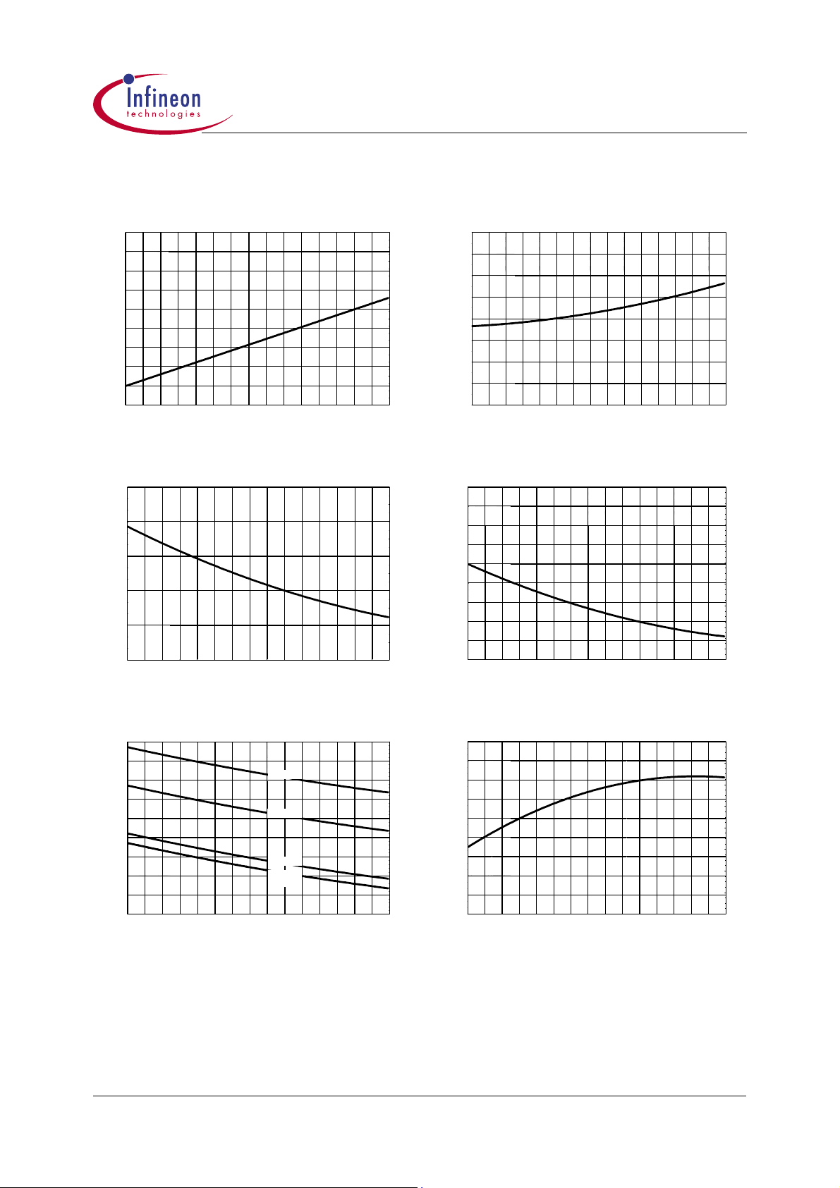
5 Typical Performance Characteristics
CoolSET™-F2
ICE2A165/265/365
ICE2A180/280
40
38
36
[µA]
34
VCC1
32
30
28
26
Start Up Current I
24
22
-25-15-5 5 152535455565758595105115125
Junction Temperature [°C]
Figure 22 St art Up Current I
6,0
5,7
VCC1
vs. T
j
[mA]
5,4
VCC2
5,1
4,8
Supply Current I
4,5
-25-15-5 5 152535455565758595105115125
Junction Temperature [°C]
13,58
13,56
[V]
13,54
CCon
13,52
PI-001-190101
13,50
13,48
13,46
13,44
VCC Turn-On Threshold V
13,42
-25-15-5 5 152535455565758595105115125
Junction Temperature [°C]
Figure 25 VCC Turn-On Threshold V
8,67
8,64
[V]
8,61
VCCoff
8,58
8,55
PI-003-190101
8,52
8,49
8,46
8,43
VCC Turn-Off Threshold V
8,40
-25 -15 -5 5 15 25 35 45 55 65 75 85 95 105 115 125
Junction Temperature [°C]
VCCon
vs. T
PI-004-190101
j
PI-005-190101
Figure 23 Static Supply Current I
9,0
8,6
8,2
[mA]
7,8
VCC3
7,4
7,0
6,6
6,2
Supply Current I
5,8
5,4
-25-15-5 5 152535455565758595105115125
ICE2A365
ICE2A280
ICE2A265
ICE2A165
ICE2A180
VCC2
vs. T
Junction Temperature [°C]
Figure 24 Supply Current I
VCC3
vs. T
j
j
Figure 26 VCC Turn-Off Threshold V
5,10
[V]
5,07
CCHY
5,04
5,01
4,98
PI-002-190101
4,95
4,92
4,89
4,86
4,83
VCC Turn-On/Off Hysteresis V
-25 -15 -5 5 15 25 35 45 55 65 75 85 95 105 115 125
Junction Temperature [°C]
Figure 27 VCC Turn-On/Off HysteresisV
VCCoff
vs. T
VCCHY
j
vs. T
Datasheet 18 September 2001
PI-006-190101
j

CoolSET™-F2
ICE2A165/265/365
ICE2A180/280
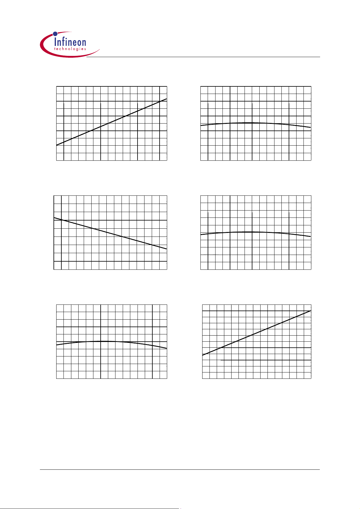
Typical Performance Characteristics
6,55
6,54
[V]
REF
6,53
6,52
6,51
6,50
6,49
6,48
6,47
6,46
Trimmed Reference Voltage V
6,45
-25 -15 -5 5 15 25 35 45 55 65 75 85 95 105 115 125
Junction Temperature [°C]
Figure 28 Trimmed Reference V
102,0
101,5
101,0
[kHz]
100,5
OSC1
100,0
99,5
99,0
98,5
98,0
97,5
Oscillator Frequency f
97,0
-25 -15 -5 5 15 25 35 45 55 65 75 85 95 105 115 125
REF
vs. T
Junction Temperature [°C]
4,70
4,68
4,66
OSC2
/f
4,64
OSC1
4,62
PI-007-190101
4,60
4,58
4,56
4,54
Frequency Ratio f
4,52
4,50
-25 -15 -5 5 15 25 35 45 55 65 75 85 95 105 115 125
PI-010-190101
Junction Temperature [°C]
j
Figure 31 Frequency Ratio f
0,730
0,728
0,726
0,724
0,722
PI-008-190101
0,720
0,718
0,716
Max. Duty Cycle
0,714
0,712
0,710
-25-15-5 5 152535455565758595105115125
OSC1
/ f
OSC2
vs. T
j
PI-011-190101
Junction Temperature [°C]
Figure 29 Oscillator Frequency f
21,8
21,7
[kHz]
21,6
OSC2
21,5
21,4
21,3
21,2
21,1
21,0
20,9
Reduced Osc. Frequency f
20,8
-25 -15 -5 5 15 25 35 45 55 65 75 85 95 105 115 125
OSC1
vs. T
Junction Temperature [°C]
Figure 3 0 Reduced Osc. Frequency f
OSC2
j
vs. T
Figure 32 Max. Duty Cycle vs. T
3,70
3,69
3,68
3,67
V
3,66
PI-009-190101
3,65
3,64
3,63
PWM-OP Gain A
3,62
3,61
3,60
-25 -15 -5 5 15 25 35 45 55 65 75 85 95 105 115 125
j
PI-012-190101
Junction Temperature [°C]
j
Figure 33 PWM-OP Gain AV vs. T
j
Datasheet 19 September 2001
CoolSET™-F2
ICE2A165/265/365
ICE2A180/280
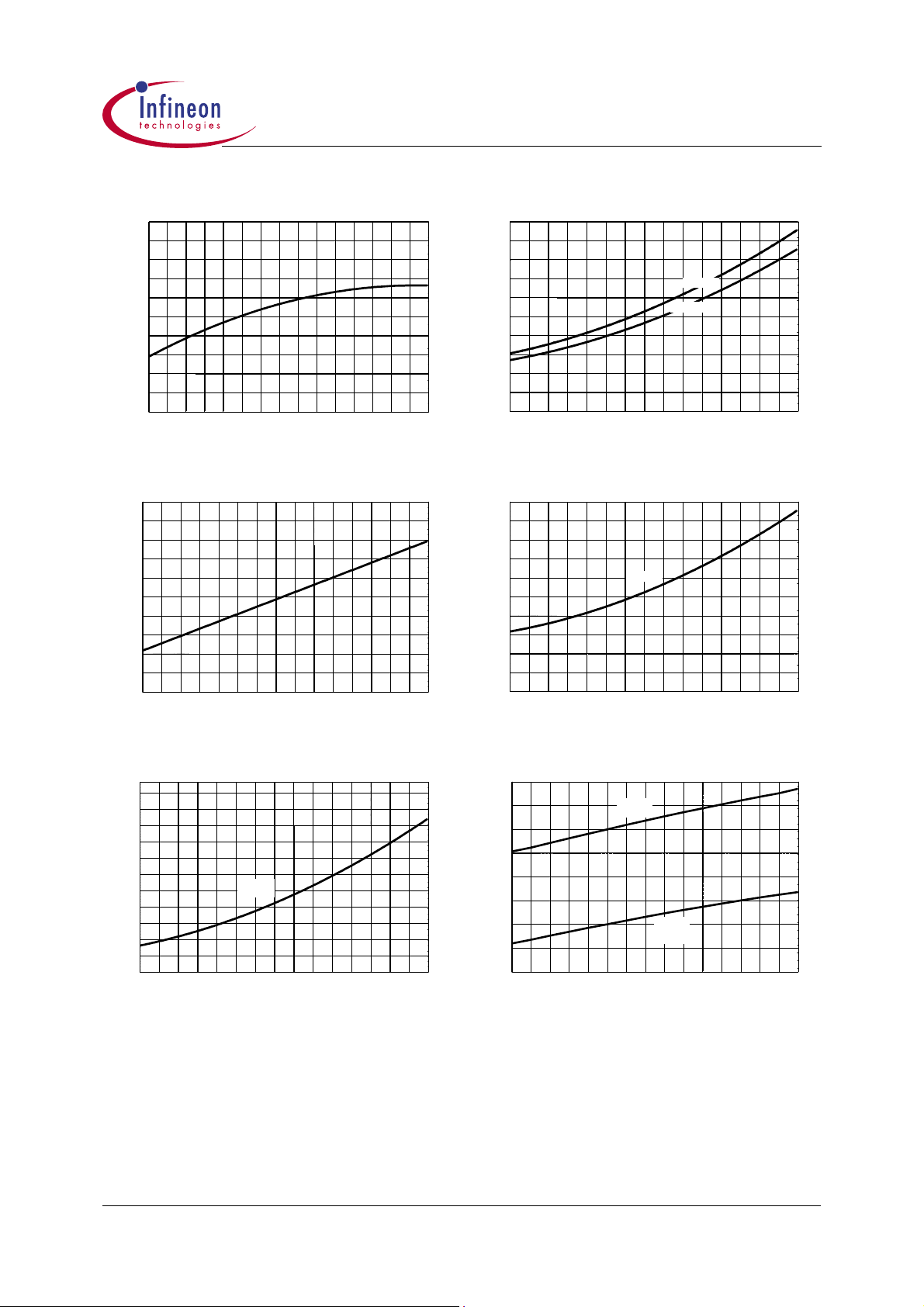
Typical Performance Characteristics
4,00
3,95
3,90
[kOhm]
3,85
FB
3,80
3,75
3,70
3,65
3,60
3,55
Feedback Resistance R
3,50
-25 -15 -5 5 15 25 35 45 55 65 75 85 95 105 115 125
Junction Temperature [°C]
Figure 34 Feedback Resistance RFB vs. T
58
56
[kOhm]
54
52
Soft-Start
50
48
46
44
42
40
Soft-Start Resistance R
-25-15-5 5 152535455565758595105115125
Junction Temperature [°C]
5,35
5,34
5,33
[V]
5,32
5,31
Soft-Start1
PI-013-190101
5,30
5,29
5,28
5,27
Detection Limit V
5,26
5,25
-25 -15 -5 5 15 25 35 45 55 65 75 85 95 105 115 125
PI-016-190101
Junction Temperature [°C]
j
Figure 37 Detection Limit V
4,05
4,04
4,03
[V]
4,02
4,01
Soft-Start2
PI-014-190101
4,00
3,99
3,98
3,97
Detection Limit V
3,96
3,95
-25 -15 -5 5 15 25 35 45 55 65 75 85 95 105 115 125
Soft-Start1
vs. T
j
PI-017-190101
Junction Temperature [°C]
Figure 35 Soft-Start Resistance R
4,85
4,84
4,83
[V]
4,82
FB2
4,81
4,80
4,79
4,78
4,77
Detection Limit V
4,76
4,75
-25-15-5 5 152535455565758595105115125
Soft-Start
Junction Temperature [°C]
Figure 36 Detection Li mit V
FB2
vs. T
j
vs. T
j
Figure 38 Detection Limit V
16,80
16,75
[V]
16,70
VCC1
16,65
16,60
16,55
PI-015-190101
16,50
16,45
16,40
16,35
16,30
16,25
16,20
Overvoltage Detection Limit V
-25-15-5 5 152535455565758595105115125
Soft-Start2
vs. T
j
PI-018-190101
Junction Temperature [°C]
Figure 39 Overvoltage Dete ction Limit V
VCC1
vs. T
j
Datasheet 20 September 2001
CoolSET™-F2
ICE2A165/265/365
ICE2A180/280
Typical Performance Characteristics
1,010
1,008
[V]
1,006
csth
1,004
1,002
1,000
0,998
0,996
0,994
0,992
Peak Current Limitation V
0,990
-25-15-5 5 152535455565758595105115125
Junction Temperature [°C]
Figure 40 Peak Current Li m i tation V
280
270
[ns]
260
LEB
250
240
230
220
210
200
190
Leading Edge Blanking t
180
-25 -15 -5 5 15 25 35 45 55 65 75 85 95 105 115 125
csth
Junction Temperature [°C]
vs. T
2,0
1,8
1,6
PI-019-190101
1,4
[Ohm]
1,2
dson
1,0
0,8
0,6
0,4
On-Resistance R
0,2
0,0
-25-15-5 5 152535455565758595105115125
ICE2A265
ICE2A280
PI-023-190101
Junction Temperature [°C]
j
Figure 43 Drain Source On-Resistance R
1,0
0,9
0,8
0,7
PI-020-190101
[Ohm]
0,6
dson
0,5
0,4
0,3
0,2
On-Resistance R
0,1
0,0
-25-15-5 5 152535455565758595105115125
ICE2A365
DSon
vs. T
j
PI-024-190101
Junction Temperature [°C]
Figure 41 Leading Edge Blanking V
7,6
7,0
6,4
5,8
[Ohm]
5,2
dson
4,6
4,0
3,4
2,8
2,2
On-Resistance R
1,6
1,0
-25 -15 -5 5 15 25 35 45 55 65 75 85 95 105 115 125
ICE2A165
ICE2A180
VCC1
Junction Temperature [°C]
Figure 42 Drain Source On-Resistance R
vs. T
DSon
j
vs. T
Figure 44 Drain Source On-Resistance R
900
850
[V]
800
(BR)DSS
750
PI-022-190101
j
700
650
600
550
Breakdown Voltage V
500
-25 -15 -5 5 15 25 35 45 55 65 75 85 95 105 115 125
Figure 45 Breakdown Voltage V
ICE2A180
ICE2A280
ICE2A165
ICE2A265
ICE2A365
Junction Temperature [°C]
BR(DSS)
DSon
vs. T
vs. T
j
j
PI-025-190101
Datasheet 21 September 2001

6 Outline Dimension
P-DIP-8-6
(Plastic Dual In-line
Package)
CoolSET™-F2
ICE2A165/265/365
ICE2A180/280
Outline Dimension
Figure 46
Dimensions in mm
Datasheet 22 September 2001

Total Quality Management
Qualität hat für uns eine umfassende
Bedeutung. Wir wollen allen Ihren
Ansprüchen in der bestmöglichen
Weise gerecht werd en. Es geht uns also
nicht nur um die Produktqualität –
unsere Anstrengungen gelten
gleichermaßen der Lieferqualität und
Logistik, dem Service und Support
sowie allen sonstigen Beratungs- und
Betreuungsleistungen.
Dazu gehört eine bestimmte
Geisteshaltung unserer Mitarbeiter.
Total Quality im Denken und Handeln
gegenüber Kollegen, Lieferanten und
Ihnen, unserem Kunden. Unsere
Leitlinie ist jede Aufgabe mit „Null
Fehlern“ zu lösen – in offener
Sichtweise auch über den eigenen
Arbeitsplatz hinaus – und uns ständig
zu verbesse rn .
Unternehmensweit orientieren wir uns
dabei auch an „top“ (Time Optimized
Processes), um Ihnen durch größere
Schnelligkeit den entscheidenden
Wettbewerbsvorspru ng zu verschaffen.
Geben Sie uns die Chance, hohe
Leistung durch umfassende Qualität zu
beweisen.
Wir werden Sie überzeugen.
Quality takes on an allencompassing
significance at Semiconductor Group.
For us it means living up to each and
every one of your demands in the best
possible way. So we are not only
concerned with product quality. We
direct our efforts equally at quality of
supply and logistics, service and
support, as well as all the other ways in
which we advise and attend to you.
Part of this is t he v ery spec i al att it ude of
our staff. Total Quality in thought and
deed, towards co-workers, suppliers
and you, our customer. Our guideline is
“do everything with zero defects”, in an
open manner that is demonstrated
beyond your immediate workplace, and
to constantly improve.
Throughout the corporation we also
think in terms of Time Optimized
Processes (top), greater speed on our
part to give you that decisive
competitive edge.
Give us the chance to prove the best of
performance through the best of quality
– you will be convinced.
http://www.infineon.com
Published by Infineon Technologies AG
 Loading...