

查询HYS72T32000GR供应商
HYS72T32000GR (2 56 MByte)
HYS72T64001GR (5 12 MByte)
HYS72T64020GR (5 12 MByte)
Data Sheet, V0.22,Feb. 2004
DDR2 Registered DIMM Modules
Memory Products
Never stop thinking.
HYS72T32000GR, HYS72T64001GR
HYS72T64020GR
Preliminary Datasheet Rev. 0.22 (2.04)
Low Profile 240-pin Registered DDR2 SDRAM Modules Datasheet
256 MByte & 512 MByte Modules
PC2-3200R /-4200R /-5300R
• 240-pin Registered 8-Byte ECC Dual-In-Line
DDR2 SDRAM Module for PC, Workstation
and Server main memory applications
• One rank 32Mb x 72, 64Mb x 72 and
two ranks 64Mb × 72 organizations
• JEDEC standard Double Data Rate 2
Synchronous DRAMs (DDR2 SDRAMs) with
+1.8V (± 0.1 V) power supply
• Modules built with 256 Mb DDR2 SDRAMs in
60-ball FBGA chipsize packages
• Programmable CAS
Burst Length (4 & 8) and Burst Type.
• Auto Refresh and Self Refresh
• All inputs and outputs SSTL_1.8 compatible
• Performance:
Speed Grade Indicator -5 -3.7 -3 Unit
Component Speed Grade on Module DDR2-400 DDR2-533 DDR2-667
Module Speed Grade PC2-3200 PC2-4200 PC2-5300
Max. Clock Frequency @ CL = 3 200 200 200 MHz
Max. Clock Frequency@ CL = 4 & 5 200 266 333 MHz
1.0 Description
The INFINEON HYS72T32000GR, HYS72T64020GR and HYS72T64001 are low profile
Registered DIMM modules with 30,00 mm height based on DDR2 technology. DIMMs are available
in 32M x 72 (256 MByte), 2 x 32M x 72 (512 MByte) and 64M x 72 (512 MByte) organisation and
density, intended for mounting into 240 pin connector sockets.
The memory array is designed with 256Mbit Double Data Rate (DDR2) Synchronous DRAMs for
ECC applications. All control and address signals are re-driven on the DIMM using register devices
and a PLL for the clock distribution. This reduces capacitive loading to the system bus, but adds one
cycle to the SDRAM timing. Decoupling capacitors are mounted on the PCB board, which pr ovide
a proper voltage supply impedance over the whole frequency range of operations as number and
values are accordant to the JEDEC specification. The DIMMs feature serial presence detect based
on a serial E
configuration data and the second 128 bytes are available to the customer.
2
PROM device using the 2-pin I2C protocol. The first 128 bytes are programmed with
Latencies (3, 4 & 5),
• Re-drive for all input signals using register
and PLL devices.
• OCD (Off-Chip Driver Impedance
Adjustment) and ODT (On-Die Termination)
• Serial Presence Detect with E
• Low Profile Modules form factor:
133.35 mm x 30,00 mm (MO-237)
• Based on JEDEC standard reference card
designs Raw Card “A”, “B” and “C”.
2
PROM
INFINEON Technologies
Rainer.Weidlich@Infineon.com 22.04
HYS72Txx0xxGR
Registered DDR2 SDRAM-Modules
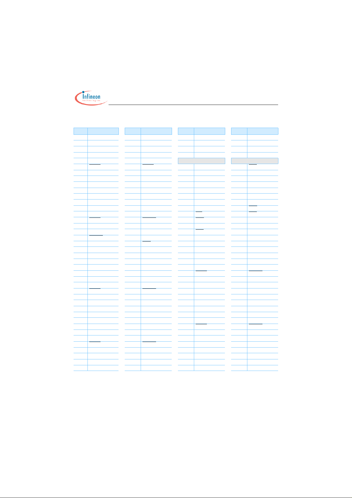
1.1 Ordering Information
Type & Partnumber Compliance Code Description SDRAM
PC2-3200 (DDR2-400):
HYS72T32000GR-5-A PC2-3200R-33310-A one rank 256 MB Reg. DIMM 256 Mbit (x8)
HYS72T64020GR-5-A PC2-3200R-33310-B two ranks 512 MB Reg. DIMM 256 Mbit (x8)
HYS72T64001GR-5-A PC2-3200R-33310-C one ranks 512 MB Reg.DIMM 256 Mbit (x4)
PC2-4200 (DDR2-533):
HYS72T32000GR-3.7-A PC2-4200R-44410-A one rank 256 MB Reg. DIMM 256 Mbit (x8)
HYS72T64020GR-3.7-A PC2-4200R-44410-B two ranks 512 MB Reg. DIMM 256 Mbit (x8)
HYS72T64001GR-3.7-A PC2-4200R-44410-C one ranks 512 MB Reg.DIMM 256 Mbit (x4)
PC2-5300 (DDR2-667):
HYS72T32000GR-3-A PC2-5300R-44410-A one rank 256 MB Reg. DIMM 256 Mbit (x8)
HYS72T64020GR-3-A PC2-5300R-44410-B two ranks 512 MB Reg. DIMM 256 Mbit (x8)
HYS72T64001GR-3-A PC2-5300R-44410-C one ranks 512 MB Reg.DIMM 256 Mbit (x4)
Notes:
1. All part numbers end with a place code, designating the silicon die revision. Example: HYS72T32000GR-5-A, indicating
Rev. A dies are used for DDR2 SDRAM components. For all INFINEON DDR2 module and component nomenclature see
section 8 of this datasheet.
2. The Compliance Code is printed on the module label and describes the speed grade, f.e. “PC2-4200R-44410-C”, where
4200R means Registered DIMM modules with 4.26 GB/sec Module Bandwidth and “44410” means CAS latency = 4, trcd
latency = 4 and trp latency = 4 using the latest JEDEC SPD Revision 1.0 and produced on the Raw Card “C”.
Technology
1.2 Address Format
Part Number DIMM
Density
HYS72T32000GR 256 MB 32Mb × 72 1 (256Mb)
HYS72T64020GR 512 MB 2 x 32Mb × 72 2 (256Mb)
HYS72T64001GR- 512 MB 64Mb x 72 1 (256Mb)
Organization Memory
Ranks
DDR2-
SDRAMs
32Mb × 8
32Mb × 8
64Mb × 4
# of
SDRAMs
# of row/bank/
column bits
9 13/2/10
18 13/2/10
18 13/2/11
INFINEON Technologies 3 2.04
1.3 Components on Modules and RawCard
HYS72Txx0xxGR
Registered DDR2 SDRAM-Modules
DIMM
Density
DRAM components
reference datasheet
PLL Register Raw Card
256 MB HYB18T256800AC 1:10, 1.8V, CU877 1:1 25-bit 1.8V SSTU32864 A
512 MB HYB18T256800AC 1:10, 1.8V, CU877 1:2 14-bit 1.8V SSTU32864 B
512 MB HYB18T256400AC 1:10, 1.8V, CU877 1:2 14-bit 1.8V SSTU32864 C
For a detailed description of all functionalities of the DRAM components on these modules see the referenced component
datasheet
1.4 Pin Definition a nd Function
Pin Name Description Pin Name Description
A[12:0] Row Address Inputs CB[7:0] DIMM ECC Check Bits
A11, A[9:0] Column Address Inputs
A10/AP Column Address Input for Auto-
Precharge
BA[1:0] SDRAM Bank Selects DQS
CK0 Clock input
CK0
RAS
CAS
WE
CS
[1:0] Chip Selects
CKE[1:0] Clock Enable
(positive line of differential pair)
Clock input
(negative line of differential pair)
Row Address Strobe SA[2:0] slave address select
Column Address Strobe V
Read/Write Input V
3)
3)
ODT[1:0] Active termina ti on cont rol lin es
DQ[63:0] Data Input/Output NC No connection
1) Active termination only applies to DQ, DQS, DQS and DM signals
2) When low, all register outputs will be driven low and the PLL clocks to the DRAM and registers will be set to low levels (the
PLL will remain synchronized with the input clock
3) CS1, ODT1 and CKE1 are used on dual rank modules only
4) Column address A11 is used on modules based on x4 organised 256Mb DDR2 components only.
4)
DQS[8:0] SDRAM low data strobes
DM[8:0] /
DQS[17:9]
SDRAM low data mask/
high data strobes
[17:0] SDRAM differential data strobes
SCL Serial bus clock
SDA Serial bus data line
DD
REF
V
SS
V
DDSPD
1) 3)
RESET Register and PLL control pin
Power (+ 1.8 V)
I/O reference supply
Ground
EEPROM power supply
2)
INFINEON Technologies 4 2.04
HYS72Txx0xxGR
Registered DDR2 SDRAM-Modules
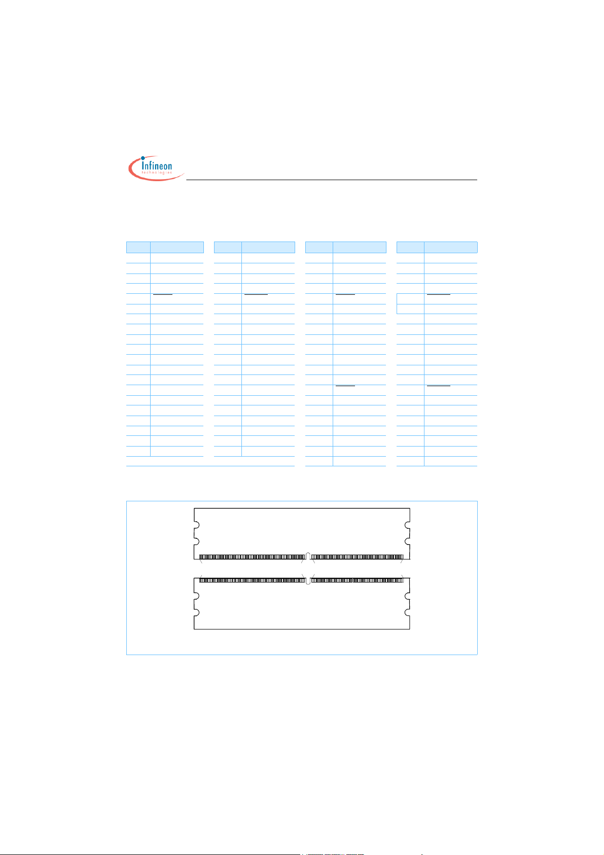
1.5 Pin Configurat ion
Symbol PIN# Symbol PIN# Symbol PIN# Symbol
PIN#
1 VREF 121 VSS 61 A4 181 VDDQ
2 VSS 122 DQ4 62 VDDQ 182 A3
3 DQ0 123 DQ5 63 A2 183 A1
4 DQ1 124 VSS 64 VDD 184 VDD
5 VSS 125 DM0, DQS9
6DQS0
7 DQS0 127 VSS 66 VSS 186 CK0
8 VSS 128 DQ6 67 VDD 187 VDD
9 DQ2 129 DQ7 68 NC 188 A0
10 DQ3 130 VSS 69 VDD 189 VDD
11 VSS 131 DQ12 70 A10/AP 190 BA1
12 DQ8 132 DQ13 71 BA0 191 VDDQ
13 DQ9 133 VSS 72 VDDQ 192 RAS
14 VSS 134 DM1, DQS10 73 WE 193 CS0
15 DQS1 135 DQS10 74 CAS 194 VDDQ
16 DQS1 136 VSS 75 VDDQ 195 ODT0
17 VSS 137 NC 76 CS1
18 RESET
19 NC 139 VSS
20 VSS 140 DQ14 79 VSS 199 DQ36
21 DQ10 141 DQ15 80 DQ32 200 DQ37
22 DQ11 142 VSS 81 DQ33 201 VSS
23 VSS 143 DQ20 82 VSS 202 DM4, DQS13
24 DQ16 144 DQ21 83 DQS4
25 DQ17 145 VSS 84 DQS4 204 VSS
26 VSS 146 DM2, DQS11 85 VSS 205 DQ38
27 DQS2
28 DQS2 148 VSS 87 DQ35 207 VSS
29 VSS 149 DQ22 88 VSS 208 DQ44
30 DQ18 150 DQ23 89 DQ40 209 DQ45
31 DQ19 151 VSS 90 DQ41 210 VSS
32 VSS 152 DQ28 91 VSS 211 DM5, DQS14
33 DQ24 153 DQ29 92 DQS5
34 DQ25 154 VSS 93 DQS5 213 VSS
35 VSS 155 DM3, DQS12 94 VSS 214 DQ46
36 DQS3
37 DQS3 157 VSS 96 DQ43 216 VSS
38 VSS 158 DQ30 97 VSS 217 DQ52
39 DQ26 159 DQ31 98 DQ48 218 DQ53
40 DQ27 160 VSS 99 DQ49 219 VSS
126 DQS9 65 VSS 185 CK0
138 NC 77 ODT1 197 VDD
78 VDDQ 198 VSS
147 DQS11 86 DQ34 206 DQ39
156 DQS12 95 DQ42 215 DQ47
KEY KEY
196 NC
203 DQS13
212 DQS14
INFINEON Technologies 5 2.04
HYS72Txx0xxGR
Registered DDR2 SDRAM-Modules
Pin Configuration (cont’d)
Symbol PIN# Symbol PIN# Symbol PIN# Symbol
PIN#
41 VSS 161 CB4 100 VSS 220 NC
42 CB0 162 CB5 101 SA2 221 NC
43 CB1 163 VSS 102 NC 222 VSS
44 VSS 164 DM8, DQS17 103 VSS 223 DM6, DQS15
45 DQS8
46 DQS8 166 VSS 105 DQS6 225 VSS
47 VSS 167 CB6 106 VSS 226 DQ54
48 CB2 168 CB7 107 DQ50 227 DQ55
49 CB3 169 VSS 108 DQ51 228 VSS
50 VSS 170 VDDQ 109 VSS 229 DQ60
51 VDDQ 171 NC, CKE1 110 DQ56 230 DQ61
52 CKE0 172 VDD 111 DQ57 231 VSS
53 VDD 173 NC 112 VSS 232 DM7, DQS16
54 NC 174 NC 113 DQS7
55 NC 175 VDDQ 114 DQS7 234 VSS
56 VDDQ 176 A12 115 VSS 235 DQ62
57 A11 177 A9 116 DQ58 236 DQ63
58 A7 178 VDD 117 DQ59 237 VSS
59 VDD 179 A8 118 VSS 238 VDDSPD
60 A5 180 A6 119 SDA 239 SA0
165 DQS17 104 DQS6 224 DQS15
233 DQS16
120 SCL 240 SA1
1.6 Pin Locations
Front
pin 1
pin 121
64
184
Backside
65
185
120
240
240 pin Modules (MO-237)
INFINEON Technologies 6 2.04
Registered DDR2 SDRAM-Modules
1.7 Registered DIMM Input/Output Functional Description
Symbol
CK0, CK
CKE[1:0]
CS[1:0]
ODT[1:0]
RAS, CAS,
DM[8:0]
BA[1:0]
A[12:0]
DQ[63:0],
CB[7:0]
DQS[17:0],
DQS
SA[2:0]
SDA
SCL
RESET
V
DD, VSS
V
V
DDSPD
Note: CS1, ODT1 and CKE1 are used on dual rank modules only.
Type Polarity Function
The system clock inputs. All address and command lines are sampled on the cross point of
0
Input Cross point
Active High
Input
Active Low
Input
Active High On-Die Termination control signals
Input
Active Low
WE
Input
Active High Masks write data when high, issued concurrently with input data.
Input
Input
Input
I/O - Data and Check Bit Input /Output pins.
I/O
[17:0]
REF
Cross point
Input
I/O -
Input
Input
Supply - Power and ground for the DDR SDRAM input buffers and core logic.
Supply - Reference voltage for the SSTL-18 inputs.
Supply -
the rising edge of CK and the falling edge of CK. An on-board DLL circuit is driven from the
clock inputs and output timing for read operations is synchronized to the input clock.
CKE high activates and CKE low deactivates internal clock signals and device input buffers
and output drivers of the SDRAMs. Taking CKE low provides Precharge Power-Down and
Self-Refresh operation (all banks idle), or Active Power-Down (row Active in any bank).
Enables the associated SDRAM command decoder when low and disables decoder when
high. When decoder is disabled, new commands are ignored and previous operations continue. The input signals also disable all outputs (except CKE and ODT) of the register(s) on
the DIMM when both inputs are high. When both CS[1:0] are high, all register outputs (except
CK, ODT and Chip select) remain in the previous state.
When sampled at the positive edge of the clock, RAS, CAS and WE define the operation to
be executed by the SDRAM.
- Selects which internal SDRAM memory bank is activated
During Bank Activate command cycle, Address defines the row address. During a Read or
Write command cycle, Address defines the column address. In addition to the column
address, A10(=AP) is used to invoke Auto-Precharge operation at the end of the burst read
or write cycle. If AP is high, Auto Precharge is selected and BA[1:0] defines the bank to be
precharged. If AP is low, Auto-Precharge is disabled. During a Precharge command cycle,
AP is used in conjunction with BA[1:0] to control which bank(s) to precharge. If AP is high, all
banks will be precharged regardless of the state of BA[1:0]. If AP is low, BA[1:0] are used to
define which bank to precharge.
The data strobes, associated with one data byte, source with data transfer. In Write mode,
the data strobe is sourced by the controller and is centered in the data window. In Read
mode the data strobe is sources by the DDR2 SDRAM and is sent at the leading edge of the
data window. DQS signals are complements, and timing is relative to the crosspoint of
respective DQS and DQS. If the module is to be operated in single ended strobe mode, all
DQS signals must be tied on the system board to VSS and DDR2 SDRAM mode registers
programmed appropriately.
These signals are tied at the system planar to either VSS or VDDSPD to configure the serial
SPD EEPROM address range
This bidirectional pin is used to transfer data into and out of the SPD EEPROM. A resistor
maybe connected from the SDA bus line to VDDSPD on the system planar to act as a pullup.
This signal is used to clock data into the SPD EEPROM. A resistor maybe connected from
the SCL bus line to VDDSPD on the system planar to act as a pull-up.
The RESET
-
When low, all register outputs will be driven low and the PLL clocks to the DRAMs and the
register(s) will be set to low level. The PLL will remain synchronized with the input clock.
Serial EEPROM positive power supply, wired to a separated power pin at the connector
which supports from 1.7 Volt to 3.6 Volt.
pin is connected to the RST pin on the register and to the OE pin on the PLL.
HYS72Txx0xxGR
INFINEON Technologies 7 2.04
HYS72Txx0xxGR
Registered DDR2 SDRAM-Modules
2.0 Block Diagrams (cont’d)
2.1 One Rank 32M x 72 (256 MByte) DDR2 SDRAM DIMM Module (x8 components)
HYS72T32000GR on Raw Card A
RS0
DQS0
DQS0
CS0 *
BA0-BA1
A0 -A12
RAS
CAS
WE
CKE0
ODT0
RESET
PCK7
PCK 7
DM0/DQS9
DQS9
DQS1
DQS1
DM1/DQS10
DQS10
DQS2
DQS0
DM2/DQS11
DQS11
DQS3
DQS3
DM3/DQS12
DQS12
DQS8
DQS8
DM8/DQS17
DQS17
CB0
CB1
CB2
CB3
CB4
CB5
CB6
CB7
RST
DQ0
DQ1
DQ2
DQ3
DQ4
DQ5
DQ6
DQ7
DQ8
DQ9
DQ10
DQ11
DQ12
DQ13
DQ14
DQ15
DQ16
DQ17
DQ18
DQ19
DQ20
DQ21
DQ22
DQ23
DQ24
DQ25
DQ26
DQ27
DQ28
DQ29
DQ30
DQ31
1:1
R
E
G
I
S
T
E
R
DM/
NU/
CS DQS
RDQS
RDQS
I/O 0
I/O 1
D0
I/O 2
I/O 3
I/O 4
I/O 5
I/O 6
I/O 7
DM/
NU/
CS DQS
RDQS
RDQS
I/O 0
I/O 1
D1
I/O 2
I/O 3
I/O 4
I/O 5
I/O 6
I/O 7
DM/
NU/
DQS
CS
RDQS
RDQS
I/O 0
I/O 1
D2
I/O 2
I/O 3
I/O 4
I/O 5
I/O 6
I/O 7
NU/
DM/
CS DQS
RDQS
RDQS
I/O 0
I/O 1
D3
I/O 2
I/O 3
I/O 4
I/O 5
I/O 6
I/O 7
DM/
NU/
CS DQS DQS
RDQS
RDQS
I/O 0
I/O 1
D8
I/O 2
I/O 3
I/O 4
I/O 5
I/O 6
I/O 7
0 -> CS : SDRAMs D0-D8
RS
RBA0-RBA1
RA0 -RA12-> A0 -A 12: SDRA Ms D0-D 8
RRA S -> RAS : SDR AMs D0- D8
RCAS -> C A S: SD RAMs D0-D8
RW E -> WE : SDRAMs D0-D8
RCKE0 -> CKE : SDRA D0-D8
RODT0 - > ODT 0: SDRAMs D0-D8
A0-BA1: SDRAMs D0-D8
-> B
*) CS0 connects to DCS and VDD connects to CSR on the Reg isters
DQS4
DQS4
DM4/DQS13
DQS
DQS
DQS
DQS
DQS13
DQS5
DQS5
DM5/DQS14
DQS14
DQS6
DQS6
DM6/DQS15
DQS15
DQS7
DQS7
DM7/DQS16
DQS16
DQ32
DQ33
DQ34
DQ35
DQ36
DQ37
DQ38
DQ39
DQ40
DQ41
DQ42
DQ43
DQ44
DQ45
DQ46
DQ47
DQ48
DQ49
DQ50
DQ51
DQ52
DQ53
DQ54
DQ55
DQ56
DQ57
DQ58
DQ59
DQ60
DQ61
DQ62
DQ63
Serial PD
SCL
A0
WP
A1 A2
SA0 SA1
SA2
CK0
CK 0
RESET
DM/
NU/
CS DQS DQS
RDQS
RDQS
I/O 0
I/O 1
D4
I/O 2
I/O 3
I/O 4
I/O 5
I/O 6
I/O 7
DM/
NU/
RDQS
I/O 0
I/O 1
I/O 2
I/O 3
I/O 4
I/O 5
I/O 6
I/O 7
NU/
RDQS
I/O 0
I/O 1
I/O 2
I/O 3
I/O 4
I/O 5
I/O 6
I/O 7
NU/
RDQS
I/O 0
I/O 1
I/O 2
I/O 3
I/O 4
I/O 5
I/O 6
I/O 7
SDA
PCK0-PCK6,PCK 8,PCK9
P
PCK0-PCK6,
L
L
PCK7
OE
PCK7
Notes:
1. DQ-to-I/O wiring may be changed within a byte
2. Unless otherwise noted, resistor values are 22 Ohms
CS DQS
RDQS
D5
DM/
DQS
CS
RDQS
D6
DM/
CS DQS
RDQS
D7
V
VREF
-> CK : Register
> CK : Register
DQS
DQS
DQS
DDSPD
V
V
DD,
DDQ
V
SS
PCK8,PCK9
CK : SDRAMs D0-D8
CK : SDRAMs D0-D8
Serial PD
D0 - D8
D0 - D8
D0 - D8
INFINEON Technologies 8 2.04

HYS72Txx0xxGR
Registered DDR2 SDRAM-Modules
Block Diagrams (cont’d)
2.2 64M x 72 (512 MByte) two rank DDR2 SDRAM DIMM Modules (x8 components)
HYS72T64020GR on Raw Card B
RS1
RS0
DQS0
DQS0
DM0/DQS9
DQS9
DQ0
DQ1
DQ2
DQ3
DQ4
DQ5
DQ6
DQ7
DQS1
DQS1
DM1/DQS10
DQS10
DQ8
DQ9
DQ10
DQ11
DQ12
DQ13
DQ14
DQ15
DQS2
DQS0
DM2/DQS11
DQS11
DQ16
DQ17
DQ18
DQ19
DQ20
DQ21
DQ22
DQ23
DQS3
DQS3
DM3/DQS12
DQS12
DQ24
DQ25
DQ26
DQ27
DQ28
DQ29
DQ30
DQ31
DQS8
DQS8
DM0/DQS17
DQS17
CB0
CB1
CB2
CB3
CB4
CB5
CB6
CB7
CS0 *
CS1 *
BA0-BA1
A0 -A12
RAS
CAS
WE
CKE0
CKE1
ODT0
ODT1
RESET
PCK7
PCK 7
*) CS0 connects to CRS, CS1 connects to CSR on a Regis ter. CS1 connects to DCS and CS0 connects to CSR on another Register.
RESET, PCK7 and PCK7 connect to bother Registe rs. Other signals connect to one of two Registers.
DM/
NU/
RDQS
RDQS
I/O 0
I/O 1
I/O 2
I/O 3
I/O 4
I/O 5
I/O 6
I/O 7
DM/
NU/
RDQS
RDQS
I/O 0
I/O 1
I/O 2
I/O 3
I/O 4
I/O 5
I/O 6
I/O 7
NU/
DM/
RDQS
RDQS
I/O 0
I/O 1
I/O 2
I/O 3
I/O 4
I/O 5
I/O 6
I/O 7
NU/
DM/
RDQS
RDQS
I/O 0
I/O 1
I/O 2
I/O 3
I/O 4
I/O 5
I/O 6
I/O 7
NU/
DM/
RDQS
RDQS
I/O 0
I/O 1
I/O 2
I/O 3
I/O 4
I/O 5
I/O 6
I/O 7
1:2
RS
RS
R
E
RB A0-RBA1 -> B
G
RA0 -RA12-> A0 -A 12: SDRA Ms
I
S
RRA S
T
E
RCAS
R
RW E
RCKE0 -> CKE :
RCKE1 -> CKE :
RODT0 - >
RODT1 - >
RST
NU/
DM/
DQS
CS DQS
RDQS
RDQS
I/O 0
I/O 1
D0
I/O 2
I/O 3
I/O 4
I/O 5
I/O 6
I/O 7
NU/
CS DQS DQS
RDQS
RDQS
I/O 0
I/O 1
D1
I/O 2
I/O 3
I/O 4
I/O 5
I/O 6
I/O 7
NU/
DM/
DQS
CS DQS
D2
DQS DQS
CS
D3
DQS DQ S
CS
D8
0 -> CS : SDRAMs D0-D8
1 -> CS : SDRAMs
-> RAS : SD RAMs
-> C AS: SDRAMs
-> WE : SDRAMs
RDQS
RDQS
I/O 0
I/O 1
I/O 2
I/O 3
I/O 4
I/O 5
I/O 6
I/O 7
NU/
RDQS
RDQS
I/O 0
I/O 1
I/O 2
I/O 3
I/O 4
I/O 5
I/O 6
I/O 7
NU/
DM/
RDQS
RDQS
I/O 0
I/O 1
I/O 2
I/O 3
I/O 4
I/O 5
I/O 6
I/O 7
D9-D17
A0-BA1 : SDRAMs
SDRAMs D0-D8
SDRAMs
: SDRAMs
ODT
ODT : SDRAMs D9-D17
DM/
DM/
D0-D17
D0-D17
D0-D17
D9-D17
D0-D8
CS
D9
CS
D10
CS
D11
CS DQS
D12
CS DQS
D17
DQS DQS
DQS
DQS
D0-D17
DQS
DQS
DQS
DQS
D0-D17
DQS4
DQS4
DM4/DQS13
DQS13
DQS5
DQS5
DM5/DQS14
DQS14
DQS6
DQS6
DM6/DQS15
DQS15
DQS7
DQS7
DM7/DQS16
DQS16
CK 0
CK
RESET
NU/
DM/
DQS
CS DQS
RDQS
V
DDSPD
V
DD,
VREF
V
SS
RDQS
I/O 0
I/O 1
D4
I/O 2
I/O 3
I/O 4
I/O 5
I/O 6
I/O 7
DM/
NU/
RDQS
I/O 0
I/O 1
I/O 2
I/O 3
I/O 4
I/O 5
I/O 6
I/O 7
NU/
RDQS
I/O 0
I/O 1
I/O 2
I/O 3
I/O 4
I/O 5
I/O 6
I/O 7
NU/
RDQS
I/O 0
I/O 1
I/O 2
I/O 3
I/O 4
I/O 5
I/O 6
I/O 7
V
DDQ
DQS
DQS
CS
RDQS
D5
DM/
DQS DQ S
CS
RDQS
D6
DM/
DQS
DQS
CS
RDQS
D7
DQ32
DQ33
DQ34
DQ35
DQ36
DQ37
DQ38
DQ39
DQ40
DQ41
DQ42
DQ43
DQ44
DQ45
DQ46
DQ47
DQ48
DQ49
DQ50
DQ51
DQ52
DQ53
DQ54
DQ55
DQ56
DQ57
DQ58
DQ59
DQ60
DQ61
DQ62
DQ63
Serial P D
SCL
A0
WP
A1
A2
SA0 SA1
SA2
PCK0-PCK6, PCK8,PCK9 CK
P
0
L
L
OE
DQ-to-I/O wiring may be changed within a by te
DQ/DQS/DQS, adress and control resistor s are 22 Ohms
PCK8,PCK9
PCK0-PCK6,
PCK7 -> CK :Register
PCK7
> CK
: Register
NU/
DM/
RDQS
RDQS
I/O 0
I/O 1
I/O 2
I/O 3
I/O 4
I/O 5
I/O 6
I/O 7
NU/
DM/
RDQS
RDQS
I/O 0
I/O 1
I/O 2
I/O 3
I/O 4
I/O 5
I/O 6
I/O 7
NU/
DM/
RDQS
RDQS
I/O 0
I/O 1
I/O 2
I/O 3
I/O 4
I/O 5
I/O 6
I/O 7
NU/
DM/
RDQS
RDQS
I/O 0
I/O 1
I/O 2
I/O 3
I/O 4
I/O 5
I/O 6
I/O 7
Serial P D
D0 - D17
D0 - D17
D0 - D17
SDA
: SDRAMs D0-D17
CK
: SDRAMs D0-D17
DQS DQS
CS
D13
CS DQS DQS
D14
DQS DQS
CS
D15
DQS
CS
D16
DQS
INFINEON Technologies 9 2.04

HYS72Txx0xxGR
Registered DDR2 SDRAM-Modules
Block Diagrams (cont’d)
2.3 One Rank 64M x 72 (512 MByte) DDR2 SDRAM DIMM Modules (x4 components)
HYS72T64001GR on Raw Card C
VSS
RS0
DQS0
DQS0
DQ0
DQ1
DQ2
DQ3
DQS1
DQS0
DQ8
DQ9
DQ10
DQ11
DQS2
DQS2
DQ16
DQ17
DQ18
DQ19
DQS3
DQS3
DQ24
DQ25
DQ26
DQ27
DQS4
DQS4
DQ32
DQ33
DQ34
DQ35
DQS5
DQS5
DQ40
DQ41
DQ42
DQ43
DQS6
DQS6
DQ48
DQ49
DQ50
DQ51
DQS7
DQS7
DQ56
DQ57
DQ58
DQ59
DQS8
DQS8
CB0
CB1
CB2
CB3
CS0 *
BA0-BA1
A0 -A12
RAS
CAS
WE
CKE0
ODT0
RESET
PCK7
PCK 7
*) CS0 connects to DCS of Register 1 and CSR of Regi ster 2,
CSR of Register 1 and DCS of Register 2 connects to VDD
**) RESET, PCK7 and PCK7 connet to both Registers.
Other signals connect to one of two Registers.
1:2
R
E
G
I
S
T
E
R
RST
DM
I/O 0
I/O 1
I/O 2
I/O 3
DM
I/O 0
I/O 1
I/O 2
I/O 3
DM
I/O 0
I/O 1
I/O 2
I/O 3
DM
I/O 0
I/O 1
I/O 2
I/O 3
DM
I/O 0
I/O 1
I/O 2
I/O 3
DM
I/O 0
I/O 1
I/O 2
I/O 3
DM
I/O 0
I/O 1
I/O 2
I/O 3
DM
I/O 0
I/O 1
I/O 2
I/O 3
DM
I/O 0
I/O 1
I/O 2
I/O 3
RS
0 -> C S : SDRAMs
RBA0 -RBA1 -> B
RA0 -RA12-> A0 -A12: SDR AMs
RRA S
RCAS
RW E
RCKE0 -> CKE :
RODT0 ->
A0-BA1: SDRAMs
-> RAS : SD RAMs
-> C AS: SD RAMs
-> W E: SDRAMs
SDRAMs
: SDRAMs
ODT
D0-D17
CS DQS DQS
D0
CS DQS
D1
DQS
CS
D2
DQS DQS
CS
D3
DQS
CS
D4
DQS DQS
CS
D5
CS DQS
D6
CS DQS
D7
DQS
CS
D8
D0-D17
D0-D17
D0-D17
D0-D17
D0-D17
DQS
DQS
DQS
DQS
DQS
DQS
D0-D17
SCL
DQS9
DQS9
DQS10
DQS10
DQS11
DQS11
DQS12
DQS12
DQS13
DQS13
DQS14
DQS14
DQS15
DQS15
DQS16
DQS16
DQS17
DQS17
DQ4
DQ5
DQ6
DQ7
DQ12
DQ13
DQ14
DQ15
DQ20
DQ21
DQ22
DQ23
DQ28
DQ29
DQ30
DQ31
DQ36
DQ37
DQ38
DQ39
DQ44
DQ45
DQ46
DQ47
DQ52
DQ53
DQ54
DQ55
DQ60
DQ61
DQ62
DQ63
CB4
CB5
CB6
CB7
I/O 0
I/O 1
I/O 2
I/O 3
I/O 0
I/O 1
I/O 2
I/O 3
I/O 0
I/O 1
I/O 2
I/O 3
I/O 0
I/O 1
I/O 2
I/O 3
I/O 0
I/O 1
I/O 2
I/O 3
I/O 0
I/O 1
I/O 2
I/O 3
I/O 0
I/O 1
I/O 2
I/O 3
I/O 0
I/O 1
I/O 2
I/O 3
I/O 0
I/O 1
I/O 2
I/O 3
DM
DM
DM
DM
DM
DM
DM
DM
DM
Serial PD
A0
WP
A1 A2
SA0 SA1 SA2
P
CK 0
CK
RESET
PCK0-PCK6, PCK8,PCK9 CK
L
0
PCK0-PCK6,
L
PCK7 -> CK
OE
PCK7
DQ-to-I/O wiring may be changed within per nibble
Unless otherwise noted, resistor v alues are 22 Ohms
D9
D10
V
DDSPD
SDA
V
DD,
VREF
V
PCK8,PCK9
: Register
> CK : Register
CS DQS DQS
CS DQS
DQS
CS
D11
DQS DQS
CS
D12
DQS
CS
D13
DQS DQS
CS
D14
CS DQS
D15
CS DQS
D16
DQS
CS
D17
V
DDQ
SS
DQS
DQS
DQS
DQS
DQS
DQS
: SDRAMs D0-D17
CK
: SDRAMs D0-D17
Serial PD
D0 - D17
D0 - D17
D0 - D17
INFINEON Technologies 10 2.04

HYS72Txx0xxGR
Registered DDR2 SDRAM-Modules
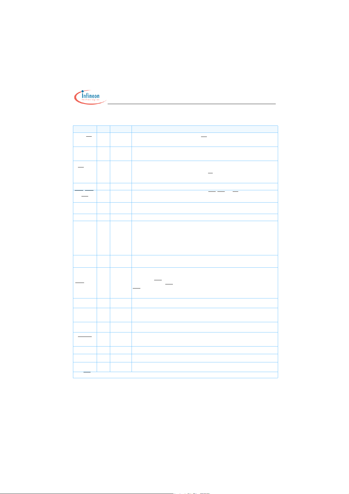
3.0 Absolute Maximum Ratings
Parameter Symbol Limit Values Unit
min. max.
Voltage on any pins relative to V
Voltage on V
Voltage on V
relative to V
DD
relative to V
DD Q
SS
SS
SS
Storage temperature range T
Stresses greater than those listed under “Absolute Maximum Ratings” may cause permanent damage to the device. This is a
stress rating only and functional operation of the device at these or any other conditions above those indicated in the operational
sections of this specification is not implied. Exposure to absolute maximum rating conditions for extended periods may affect reliability.
3.1 Operating Temperature Range
Parameter Symbol Limit Values Unit Notes
DIMM Module Operating Temperature Range (ambient) TOPR 0+55oC
DRAM Component Case Temperature Range TCASE 0+95
1. DRAM Component Case Temperature is the surface temperature in the center on the top side of any of the DRAMs. For
measurement conditions, please refer to the JEDEC document JESD51-2.
2. Within the DRAM Component Case Temperature range all DRAM specification will be supported.
3. Above 85oC DRAM case temperature the Auto-Refresh command interval has to be reduced to tREFI = 3.9 µs.
4. Self-Refresh period is hard-coded in the DRAMs and therefore it is im perativ e that the system ensu res the DRAM is below
85oC case temperature before initiating self-refresh operation.
V
IN, VOUT
V
DD
V
DDQ
STG
– 0.5 2.3 V
– 1.0 2.3 V
– 0.5 2.3
-55 +100oC
min. max.
o
C1 - 4
3.2 Supply Voltage Levels and DC Operating Conditions
Parameter Symbol Limit Values Unit Notes
min. nom. max.
Device Supply Voltage V
Output Supply Voltage V
Input Reference Voltage V
EEPROM Supply Voltage V
DC Input Logic High V
DC Input Logic Low V
In / Output Leakage Current I
1 Under all conditions, V
2 Peak to peak AC noise on V
3 For any pin on the DIMM connector under test input of 0 V ≤ VIN≤ V
DDQ
DD
DDQ
REF
DDSPD
IH (DC)
IL (DC)
L
must be less than or equal to V
may not exceed ± 2% V
REF
1.7 1.8 1.9 V -
1.7 1.8 1.9 V 1)
0.49 x V
DDQ
0.5 x V
DDQ
0.51 x V
DDQ
1.7 – 3.6 V
V
+0.125 – V
REF
– 0.30 – V
+0.3 V
DDQ
–0.125 V
REF
– 5 – 5 µA3)
DD
REF (DC).VREF
is also expected to track noise variations in V
+0.3V.
DDQ
V2)
.
DDQ
INFINEON Technologies 11 2.04

HYS72Txx0xxGR
Registered DDR2 SDRAM-Modules
4.0 IDD Specifications and Conditions
4.1 256MByte Registered Module HYS72T32000GR (one rank, nine componen ts x8)
256 MByte HYS72T32000GR PC2-3200 “-5” PC2-4200 “-3.7” PC2-5300 “-3”
Symbol Parameter / Condition
Operating Current
I
DD0
Operating Current
I
DD1
Precharge PD Standby Current
I
DD2P
Precharge Standby Current
I
DD2N
Precharge Quiet Standby Current
I
DD2Q
Active PD Standby Current
I
DD3P(0)
LP Active PD Standby Current
I
DD3P(1)
Active Standby Current
I
DD3N
Operating Current Burst Read
I
DD4R
Operating Current Burst Write
I
DD4W
Auto-Refresh Current (tRFCmin.)
I
DD5B
Auto-Refresh Current (tREFI)
I
DD5D
Self-Refresh Current
I
DD6
Operating Current
I
DD7
Note: 1) Calculated values from component data. ODT disabled. IDD1, IDD4R, and IDD7 are defined with the outputs disabled.
Currents includes Registers and PLL.
max. max. max.
Unit Note
700 828 957 mA
745 873 1002 mA
286 369 453 mA
502 657 822 mA
430 558 687 mA
367 477 597 mA
286 369 867 mA
520 648 777 mA
790 963 1137 mA
880 1098 1317 mA
970 1098 1227 mA
304 387 471 mA
36 36 36 mA
1375 1548 1722 mA
1
1
1
1
1
1
1
1
1
1
1
1
1
1
4.2 512 MByte Registered Module HYS72T64020GR (two ranks, eighteen components x8)
512 MByte HYS72T64020GR PC2-3200 “-5” PC2-4200 “-3.7” PC2-5300 “-3”
Symbol Parameter / Condition
Operating Current
I
DD0
Operating Current
I
DD1
Precharge PD Standby Current
I
DD2P
Precharge Standby Current
I
DD2N
Precharge Quiet Standby Current
I
DD2Q
Active PD Standby Current
I
DD3P(0)
LP Active PD Standby Current
I
DD3P(1)
Active Standby Current
I
DD3N
Operating Current Burst Read
I
DD4R
Operating Current Burst Write
I
DD4W
Auto-Refresh Current (tRFCmin.)
I
DD5B
Auto-Refresh Current (tREFI)
I
DD5D
Self-Refresh Current
I
DD6
Operating Current
I
DD7
Notes: 1) Calculated values from component data. ODT disabled. IDD1, IDD4R, and IDD7 are defined with the outputs disabled.
Currents includes Registers and PLL.
2) The other rank is in IDD2P Precharge Power-Down Standby Current mode
3) Both ranks are in the same IDD current mode
max. max. max.
Unit Note
854 1021 1190 mA
899 1066 1235 mA
440 562 686 mA
872 1138 1424 mA
728 940 1154 mA
602 778 974 mA
440 562 686 mA
908 1120 1334 mA
944 1156 1370 mA
1034 1291 1550 mA
1126 1291 1460 mA
476 598 722 mA
72 72 72 mA
1529 1741 1955 mA
1, 2
1, 2
1, 3
1, 3
1, 3
1, 3
1, 3
1, 3
1, 2
1, 2
1, 2
1, 3
1, 3
1, 2
INFINEON Technologies 12 2.04

HYS72Txx0xxGR
Registered DDR2 SDRAM-Modules
4.3 512 Mbyte Registered Module HYS72T64001GR (one rank, eighteen components x4)
512 MByte HYS72T64001GR PC2-3200 “-5” PC2-4200 “-3.7” PC2-5300 “-3”
Symbol Parameter / Condition
Operating Current
I
DD0
Operating Current
I
DD1
Precharge PD Standby Current
I
DD2P
Precharge Standby Current
I
DD2N
Precharge Quiet Standby Current
I
DD2Q
Active PD Standby Current
I
DD3P(0)
LP Active PD Standby Current
I
DD3P(1)
Active Standby Current
I
DD3N
Operating Current Burst Read
I
DD4R
Operating Current Burst Write
I
DD4W
Auto-Refresh Current (tRFCmin.)
I
DD5B
Auto-Refresh Current (tREFI)
I
DD5D
Self-Refresh Current
I
DD6
Operating Current
I
DD7
Note: 1) Calculated values from component data. ODT disabled. IDD1, IDD4R, and IDD7 are defined with the outputs disabled.
Currents includes Registers and PLL.
max. max. max.
Unit Note
1268 1480 1694 mA
1358 1570 1784 mA
440 562 686 mA
872 1138 1424 mA
728 940 1154 mA
602 778 974 mA
440 562 686 mA
908 1120 1334 mA
1448 1750 2054 mA
1628 2020 2414 mA
1808 2020 2234 mA
476 598 722 mA
72 72 72 mA
2618 2920 3224 mA
1
1
1
1
1
1
1
1
1
1
1
1
1
1
INFINEON Technologies 13 2.04

HYS72Txx0xxGR
Registered DDR2 SDRAM-Modules
4.4 IDD Measurement Conditions
Symbol Parameter/Condition
Operating Current - One bank Active - Precharge
tCK = tCK(IDD), tRC = tRC(IDD), tRAS = tRASmin(IDD), CKE is HIGH, CS is high between valid commands. Address and
I
DD0
control inputs are SWITCHING, Databus inputs are SWITCHING.
Operating Current - One bank Active - Read - Precharge
IOUT = 0 mA, BL = 4, tCK = tCK(IDD), tRC = tRC(IDD), tRAS = tRASmin(IDD),tRCD = tRCD(IDD),AL = 0, CL = CL(IDD);
I
DD1
CKE is HIGH, CS
SWITCHING.
Precharge Power-Down Current: All banks idle; CKE is LOW; tCK = tCK(IDD);
I
DD2P
Other control and address inputs are STABLE, Data bus inputs are FLOATING.
Precharge Standby Current: All banks idle; CS is HIGH; CKE is HIGH; tCK = tCK(IDD);
I
DD2N
Other control and address inputs are SWITCHING, Data bus inputs are SWITCHING.
Precharge Quiet Standby Current: All banks idle; CS is HIGH; CKE is HIGH; tCK = tCK(IDD);
I
DD2Q
Other control and address inputs are STABLE, Data bus inputs are FLOATING.
Active Power-Down Current: All banks open; tCK = tCK(IDD), CKE is LOW; Other control and address inputs are STA-
I
DD3P(0)
BLE, Data bus inputs are FLOATING. MRS A12 bit is set to “0” (Fast Power-down Exit);
Active Power-Down Current: All banks open; tCK = tCK(IDD), CKE is LOW; Other control and address inputs are STA-
I
DD3P(1)
BLE, Data bus inputs are FLOATING. MRS A12 bit is set to “1” (Slow Power-down Exit);
Active Standby Current: All banks open; tCK = tCK(IDD); tRAS = tRASmax(IDD); tRP = tRP(IDD),CKE is HIGH; CS is high
I
DD3N
between valid commands. Other control and address inputs are SWITCHING, Data bus inputs are SWITCHING.
Operating Current - Burst Read: All banks open; Continuous burst reads; BL = 4;AL = 0, CL = CL(IDD); tCK = tCK(IDD);
tRAS = tRASmax(IDD), tRP = tRP(IDD); CKE is HIGH, CS is high between valid commands.
I
DD4R
Address inputs are SWITCHING; Data Bus inputs are SWITCHING; IOUT = 0mA.
Operating Current - Burst Write: All banks open; Continuous burst writes; BL = 4; AL = 0, CL = CL(IDD); tCK = tCK(IDD);
tRAS = tRASmax(IDD), tRP = tRP(IDD); CKE is HIGH, CS is high between valid commands.
I
DD4W
Address inputs are SWITCHING; Data Bus inputs are SWITCHING;
Burst Auto-Refresh Current: tCK = tCK(IDD), Refresh command every tRFC = tRFC(IDD) interval, CKE is HIGH, CS is
I
DD5B
HIGH between valid commands, Other control and address inputs are SWITCHING, Data bus inputs are SWITCHING.
Distributed Auto-Refresh Current: tCK = tCK(IDD), Refresh command every tRFC = tREFI interval, CKE is LOW and CS
I
DD5D
is HIGH between valid commands, Other control and address inputs are SWITCHING, Data bus inputs are SWITCHING.
Self-Refresh Current: CKE ≤ 0.2V; external clock off, CK and CK at 0V; Other control and address inputs are FLOATING,
I
DD6
Data bus inputs are FLOATING. RESET = Low. IDD6 current values are guaranteed up to TCASE of 85oC max.
All Bank Interleave Read Current:
1. All banks interleaving reads, IOUT = 0 mA; BL = 4, CL=CL(IDD), AL = tRCD(IDD) -1*tCK(IDD);
tCK = tCK(IDD), tRC = tRC(IDD), tRRD = tRRD(IDD); CKE is HIGH, CS
inputs are STABLE during DESELECTS; Data bus is SWITCHING.
2. Timing pattern:
I
DD7
3. Legend: A = Activate, RA = Read with Auto-Precharge, D=DESELECT
Notes:
1. IDD specifications are tested after the device is properly initialized and IDD parameter are specified with ODT disabled.
2. Definitions for IDD:
LOW is defined as VIN <= VIL(ac)max; HIGH is defined as VIN >= VIH(ac)min.
STABLE is defined as inputs are stable at a HIGH or LOW level.
FLOATING is defined as inputs are VREF = VDDQ / 2.
SWITCHING is defined as:
inputs are changing between HIGH and LOW every other clock (once per two cycles) for address and control signals, and
inputs changing between HIGH and LOW every other data transfer (once per cycle) for DQ signals not including mask or
strobes.
3. IDD1, IDD4R, and IDD7 current measurements are defined with the outputs disabled (Iout = 0 mA). To achieve this on module level
the output buffers can be disabled using an EMRS(1) (Extended Mode Register Command) by setting A12 bit to HIGH.
3. For two rank modules: For all active current measurements the other rank is in Precharge Power-Down Mode IDD2P
4. RESET signal is high for all currents, except for IDD6 “Self Refresh”.
5. All current measurements includes Register and PLL current consumption.
is high between valid commands. Address and control inputs are SWITCHING, Databus inputs are
is high between valid commands, Address bus
- DDR2 -400: A0 RA0 A1 RA1 A2 RA2 A3 RA3 D D D D
- DDR2 -533: A0 RA0 D A1 RA1 D A2 RA2 D A3 RA3 D D D D D
- DDR2 -667: A0 RA0 D D A1 RA1 D D A2 RA2 D D A3 RA3 D D D D D
INFINEON Technologies 14 2.04

Registered DDR2 SDRAM-Modules
4.5 IDD Measurement Conditions (cont’d)
For testing the IDD parameters, the following timing parameters are used:
HYS72Txx0xxGR
-5
Parameter Symbol
CAS Latency CL(IDD) 3 4 4 tCK
Clock Cycle Time tCK(IDD) 5 3.75 3 ns
Active to Read or Write delay tRCD(IDD) 15 15 12 ns
Active to Active / Auto-Refresh command period tRC(IDD) 60 60 57 ns
Active bank A to Active bank B command delay tRRD(IDD) 7.5 7.5 7.5 ns
Active to Precharge Command
Precharge Command Period tRP(IDD) 15 15 12 ns
Auto-Refresh to Active / Auto-R ef resh co mmand
period
Average periodic Refresh interval tREFI 7.8 7.8 7.8 µs
tRASmin(IDD) 45 45 45 ns
tRASmax(IDD) 70000 70000 70000 ns
tRFC(IDD) 75 75 75 ns
PC2-3200
3-3-3 4-4-4 4-4-4
-3.7
PC2-4200-3PC2-5300
Unit
4.5 ODT (On Die Termination) Current
The ODT function adds additional current consumption to the DDR2 SDRAM when enabled by the EMRS(1).
Depending on address bits A6 & A2 in the EMRS(1) a “week” or “strong” termination can be selected. The current consumption for any terminated input pin, depends on the input pin is in tri-state or driving “0” or “1”, as long
a ODT is enabled during a given period of time.
ODT current per terminated pin:
EMRS(1) State
Enabled ODT current per DQ
added IDDQ current for ODT enabled;
ODT is HIGH; Data Bus inputs are FLOATING
Active ODT current per DQ
added IDDQ current for ODT enabled;
ODT is HIGH; worst case of Data Bus inputs
are STABLE or SWITCHING.
note: For power consumption calculations the ODT duty cycle has to be taken into account
A6 = 0, A2 = 1 5 6 7 .5 mA/DQ
IODTO
A6 = 1, A2 = 0 2.5 3 3.75 mA/DQ
A6 = 0, A2 = 1 10 12 15 mA/DQ
IODTT
A6 = 1, A2 = 0 5 6 7 .5 mA/DQ
min. typ. max.
Unit
INFINEON Technologies 15 2.04

HYS72Txx0xxGR
Registered DDR2 SDRAM-Modules
5.0 Electr ical Charac teristics & A C Timings
5.1 AC Timing Parameter by Spe ed Grade (Component level data, for reference only)
-5
Symbol Parameter
DQ output access time from CK / CK − 600 + 600 -500 +500 -450 +450 ps
t
AC
DQS output access time from CK / CK − 500 + 500 −450 +450 -400 +400 ps
t
DQSCK
CK, CK high-level width 0.45 0.55 0.45 0.55 0.45 0.55 t
t
CH
CK, CK low-level width 0.45 0.55 0.45 0.55 0.45 0.55 t
t
CL
Clock Half Period min. (t
t
HP
Clock cycle time
t
CK
Address and control input setup time 600 - 600 - tbd. - ps
t
IS
Address and control input hold time 600 - 600 - tbd. - ps
t
IH
DQ and DM input setup time 400 - 350 - 300 - ps
t
DS
DQ and DM input hold time 400 - 350 - 300 - ps
t
DH
Control and Addr. input pulse width (each input) 0.6 - 0.6 - 0.6 - t
t
IPW
DQ and DM input pulse width (each input) 0.35 - 0.35 - 0.35 - t
t
DIPW
Data-out high-impedance time from CK / CK -tACmax-tACmax-tACmaxps
t
HZ
DQ low-impedance from CK / CK 2*tACmin tACmax 2*tACmin tACmax 2*tACmin tACmax ps
t
LZ(DQ)
DQS low-impedance from CK / CK tACmin tACmax tACmin tACmax tACmin tACmax ps
t
LZ(DQS)
DQS-DQ skew
t
DQSQ
(for DQS & associated DQ signals)
Data hold skew factor - 450 - 400 - 350 ps
t
QHS
Data Output hold time from DQS
t
QH
Write command to 1st DQS latching transition
t
DQSS
DQS input low (high) pulse width (write cycle) 0.35 - 0.35 - 0.35 - t
t
DQSL,H
DQS falling edge to CLK setup time
t
DSS
(write cycle)
DQS falling edge hold time from CLK
t
DSH
(write cycle)
Mode register set command cycle time 2 - 2 - 2 - t
t
MRD
Write preamble 0.25 - 0.25 - 0.35 - t
t
WPRE
Write postamble 0.40 0.60 0.40 0.60 0.40 0.60 t
t
WPST
Read preamble 0.9 1.1 0.9 1.1 0.9 1.1 t
t
RPRE
Read postamble 0.400.600.400.600.400.60t
t
RPST
Active to Precharge command 45 70000 45 70000 45 70000 ns
t
RAS
Active to Active/Auto-refresh command period 60 - 60 - 57 - ns
t
RC
Auto-refresh to Active/Auto-refresh command
t
RFC
period
CL = 3 5000 8000 5000 8000 5000 8000 ps
CL = 4 & 5 5000 8000 3750 8000 3000 8000 ps
DDR2 -400
Min Max Min Max Min Max
CL, tCH)
-350-300-250ps
tHP-t
WL
-0.25WL+0.25WL-0.25WL+0.25WL-0.25WL+0.25
0.2 - 0.2 - 0.2 - t
0.2 - 0.2 - 0.2 - t
75 - 75 - 75 - ns
QHS
-tHP-t
-3.7
DDR2 -533
min. (t
CL, tCH)
QHS
-tHP-t
-3
DDR2 -667
min. (t
QHS
CL, tCH)
Unit
CK
CK
CK
CK
t
CK
CK
CK
CK
CK
CK
CK
CK
CK
INFINEON Technologies 16 2.04

HYS72Txx0xxGR
Registered DDR2 SDRAM-Modules
Symbol Parameter
-5
DDR2 -400
-3.7
DDR2 -533
-3
DDR2 -667
Unit
Min Max Min Max Min Max
Active to Read or Write delay (with and without
t
RCD
Auto-Precharge) delay
Precharge command period 15 - 15 - 12 - ns
t
RP
Active bank A to Active bank B command
t
RRD
(1k page size)
CAS A to CAS B Command Period 2-2-2-t
t
CCD
Write recovery time 15 - 15 - 15 - ns
t
WR
Auto precharge write recovery + precharge time WR+tRP - WR+tRP - WR+tRP - t
t
DAL
Internal write to read command delay 10 - 7.5 - 7.5 - ns
t
WTR
Internal read to precharge command delay 7.5 - 7.5 - 7.5 - ns
t
RTP
Exit power down to any valid command
t
XARD
(other than NOP or Deselect)
Exit active power-down mode to read command
t
XARDS
(slew exit, lower power)
Exit precharge power-down to any valid com-
t
XP
mand (other than NOP or Deselect)
Exit Self-Refresh to read command 200 - 200 - 200 - t
t
XSRD
Exit Self-Refresh to non-read command tRFC + 10 - tRFC + 10 - tRFC + 10 - ns
t
XSNR
CKE minimum high and low pulse width 3 - 3 - 3 - t
t
CKE
OCD drive mode output delay 0 12 0 12 0 12 ns
t
OIT
Minimum time clocks remain ON after CKE
t
DELAY
asynchronously drops low
Average Periodic
t
REFI
Refresh Interval
1. For details and notes see the relevant INFINEON component datasheet
2. Timing definition and values for tis, tih, tds and tdh may change due to actual JEDEC work. This may also effect the SPD code
for these parameters.
0oC - 85oC - 7.8 - 7.8 - 7.8
85oC - 95oC - 3.9 - 3.9 - 3.9
15 - 15 - 12 - ns
7.5 - 7.5 - 7.5 - ns
2-2-2-t
6 - AL - 6 - AL - 6 - AL - t
2-2-2-t
tIS+tCK
+tIH
tIS+tCK
-
+tIH
tIS+tCK
-
+tIH
-ns
CK
CK
CK
CK
CK
CK
CK
µs
5.2 ODT AC Electri cal Characteristics and Operating Conditions (all speed bins)
Symbol Parameter / Condition min. max. Units
ODT turn-on delay 2 2
t
AOND
ODT turn-on
t
AON
ODT turn-on (Power-Down Modes) tAC(min) + 2 ns 2 tCK + tAC(max) + 1 ns
t
AONPD
ODT turn-off delay 2.5 2.5
t
AOFD
ODT turn-off tAC(min) tAC(max) + 0.6 ns
t
AOF
ODT turn-off delay (Power-Down Modes) tAC(min) + 2 ns 2.5 tCK + tAC(max) + 1 ns
t
AOFPD
ODT to Power Down Mode Entry Latency 3 -
t
ANPD
ODT Power Down Exit Latency 8 -
t
AXPD
DDR2-400/533 tAC(min) tAC(max) + 1 ns
DDR2-667 tAC(min) tAC(max) + 0.7 ns
t
CK
ns
ns
t
CK
ns
ns
t
CK
t
CK
INFINEON Technologies 17 2.04

Registered DDR2 SDRAM-Modules
6.0 Serial Presence Detect Codes for Registered DIMM Modules
HYS72Txx0xxGR
Byte# Description Speed
Note:
“-5 ” := DDR2-3200 (DDR2-400)
“-3.7” := DDR2-4200 (DDR2-533)
“-3 ” := DDR2-5300 (DDR2-667)
0 Number of SPD Bytes all 128 80
1 Total Bytes in Serial PD all 256 08
2 Memory Type all DDR2-SDRAM 08
3 Number of Row Addresses all 13 0D
4 Number of Column Addresses all 10 / 11 0A 0A 0B
5 Number of DIMM Ranks, Package and Height all 1 / 2 60 61 60
6 Module Data Width al l x72 48
7 Not used all not used 00
8 Module Interface Levels all SSTL_1.8 05
9 Min. Clock Cycle Time at CAS Latency = 5 -5 5 ns 50
10 SDRAM Access Time from Clock at CL = 5 -5 0.6 ns 60
11 DIMM Configuration Type all ECC 02
12 Refresh Rate/Type all 7.8 µs / SR 82
13 SDRAM Width, Primary all x8, x4 08 08 04
14 Error Checking SDRAM Data Width all x8, x4 08 08 04
15 Not used all not used 00
16 Burst Length Supported all 4 & 8 0C
17 Number of SDRAM Banks all 4 04
18 Supported CAS Latencies all 5, 4, 3 38
19 Not used all not used 00
20 DIMM Type Information all Reg. DIMM 01
21 SDRAM Module Attributes all see note 1 00
22 SDRAM Device Attributes: General all incl. weak driver 01
23 Min. Clock Cycle Time at CAS Latency= 4 -5 5 ns 50
24 SDRAM Access Time from Clock at CL = 4 -5 0.6 ns 60
25 Min. Clock Cycle Time at CAS Latency = 3 all 5 ns 50
26 SDRAM Access Time from Clock at CL = 3 all 0.6 ns 60
27 Minimum Row Precharge Time (tRP) -5 & -3.7 15 ns 3C
28 Minimum Row Act. to Row Act. Delay (tRRD) all 7.5 ns 1E
29 Minimum RAS to CAS Delay (tRCD) -5 & -3.7 15 ns 3C
30 Minimum RAS Pulse Width (tRAS) all 45 ns 2D
31 Module Density (per rank) all 40 40 80
Grade
SPD Entry
Value
-3.7 3.7 ns 3D
-3 3 ns 30
-3.7 0.5 ns 50
-3 0.45 ns 45
-3.7 3.7 ns 3D
-3 3 ns 30
-3.7 0.5 ns 50
-3 0.45 ns 45
-3 12 ns 30
-3 12 ns 30
Hex Value
HYS72T32000GR
HYS72T64020GR
HYS72T64001GR
INFINEON Technologies 18 2.04

HYS72Txx0xxGR
Registered DDR2 SDRAM-Modules
Byte# Description Speed
Note:
“-5 ” := DDR2-3200 (DDR2-400)
“-3.7” := DDR2-4200 (DDR2-533)
“-3 ” := DDR2-5300 (DDR2-667)
32 Address and Command Setup Time (tIS) -5 0.60 ns 60
33 Address and Command Hold Time (tIH) -5 0.60ns 60
34 Data Input Setup Time (tDS) -5 0.40 ns 40
35 Data Input Hold Time (tDH) -5 0.40 ns 40
36 Write Recovery Time (tWR) all 15 ns 3C
37 Internal Write to Read Command delay (tWTR) -5 10 ns 28
38 Internal Read to Precharge delay (tRTP) all 7.5 ns 1E
39 Not used not used 00
40 Extension of Byte 41 tRC and Byte 42 tRFC all 00
41 Minimum Core Cycle Time (tRC) -5 & -3.7 60 ns 3C
42 Min. Auto Refresh Command Cycle Time (tRFC) all 75 ns 4B
43 Maximum Clock Cycle Time tck all 8 ns 80
44 Max. DQS-DQ Skew (tDQSQmax.) -5 0.35 ns 23
45 Read Data Hold Skew Factor (tQHS) -5 0.45 ns 2D
46 PLL Relock Time 15.0 µs 0F
47-61 Reserved for “Delta Temperature in SPD” see note 1 00
62 SPD Revision Revision 1.0 10
63 Checksum for Bytes 0 - 62 -5 7D 7E B6
64 Manufacturers JEDEC ID Code INFINEON C1
65-71 Not used not used 00
72 Module Assembly Location XX
73-90 Module Part Number XX
91-92 Module Revision Code XX
93-94 Module Manufacturing Date Year/Week Code XX
95-98 Module Serial Number Serial Number XX
99-127 Manufacturer’s Specific Data blank FF
128-255 Open for Customer use blank
Note 1 : Will be used for future SPD Code Revisions. For details of “Delta Temperature in SPD” see JEDEC ballot JC-
42.5 Item # 1468.
Grade
-3.7 0.35 ns 35
-3.7 0.35 ns 35
-3.7 & -3 7.5 ns 1E
SPD Entry
Value
-3.7 0.50 ns 50
-3 0.45 ns 45
-3.7 0.50 ns 50
-3 0.45ns 45
-3 0.30 ns 30
-3 0.30 ns 30
-3 57 ns 39
-3.7 0.30 ns 1E
-3 0.25 ns 19
-3.7 0.40 ns 28
-3 0.35 ns 23
-3.7 tbd. tbd. tbd.
-3 tbd. tbd. tbd.
HYS72T32000GR
Hex Value
HYS72T64020GR
HYS72T64001GR
INFINEON Technologies 19 2.04

7.0 Package Outline
7.1 Raw Card A
Module Package
DDR2 Registered DIMM Modules Raw Card A
one physical rank, 9 components x8 organised
Front View
HYS72Txx0xxGR
Registered DDR2 SDRAM-Modules
+ 0.15
-
133.35
2.7 max.
4.0
30.0.
5,175
17.80
pin 1
pin 121
10.0
3
Detail of Contacts A
-
+ 0.15
0.20
Register
PLL
64
5.0
Backside View
184
Detail of Con tacts B
65
185
55,0
5.0
0.75R
1.5
2.5
63,0
-
+ 0.20
2.50
+ 0.05
-
0.8
1.0
120
240
3
3.8 typ.
5,175
+ 0.1
-
1.27
PCB warpage 0.40
note: all outline dimensions and tolerances are in accordance with the JEDEC standard (MO-237)
INFINEON Technologies 20 2.04

7.2 Raw Card B
Module Package
DDR2 Registered DIMM Modules Raw Card B
two one physical rank, 18 components x8 organised
+ 0.15
-
133.35
Front View
HYS72Txx0xxGR
Registered DDR2 SDRAM-Modules
4.0 max.
4.0
30.0.
5,175
17.80
pin 1
pin 121
10.0
3
D e tail o f C on ta cts A
-
+ 0.15
0.20
1.0
63,0
0.8
+ 0.20
2.50
+ 0.05
-
-
Register
64
5.0
Backside View
184
Register
De ta il of Co nta c ts B
PLL
65
185
2.5
5.0
1.5
55,0
0.75R
3.8 typ.
120
240
3
5,175
+ 0.1
-
1.27
PCB warpage 0.40
note: all outline dimensions and tolerances are in accordance with the JEDEC standard (MO-237)
INFINEON Technologies 21 2.04

7.3 Raw Card C
Module Package
DDR2 Registered DIMM Modules Raw Card C
one physical rank, 18 components x4 organised
133.35
Front View
HYS72Txx0xxGR
Registered DDR2 SDRAM-Modules
+ 0.15
-
4.0 max.
4.0
30.0.
5,175
17.80
pin 1
pin 121
10.0
3
D e tail o f C on ta cts A
-
+ 0.15
0.20
1.0
63,0
0.8
+ 0.20
2.50
+ 0.05
-
-
Register
64
5.0
Backside View
184
Register
De ta il of Co nta c ts B
PLL
65
185
2.5
5.0
1.5
55,0
0.75R
3.8 typ.
120
240
3
5,175
+ 0.1
-
1.27
PCB warpage 0.40
note: all outline dimensions and tolerances are in accordance with the JEDEC standard (MO-237)
INFINEON Technologies 22 2.04

8.0 Nomenclature (Modules & Components )
8.1 DDR2 DIMM Modules
1
234567891011
Example:
HYS72Txx0xxGR
Registered DDR2 SDRAM-Modules
20GR- 5-A6 4 T 0H Y S 6 4
INFINEON Prefix HYS for DIMM Modules
1
Module Data Width
2
DRAM Technology
3
Memory Density per I/O
4
Raw Card Generation 0 = first generation 11 Die Revision
5
Number of Memory
6
Ranks
64 = Non-ECC Modules
72 = ECC Modules
T = DDR2
32 = 32 Mb
64 = 64 Mb
128 = 128 Mb
256 = 256 Mb
0 = One Rank
2 = Two Ranks
7
8
9
10 Speed Grade
Multiplying “Memory Density per I/O” with “Module Data Width”
and dividing by 8 for Non-ECC and 9 for ECC modules gives the
overall module memory density in MBytes.
8.2 DDR2 Memory Components
1 23456789
Example:
INFINEON
1
Component Prefix
Power Supply Voltage 18 = 1.8 V Power Supply
2
DRAM Technology T = DDR2
3
Memory Density
4
Memory Organisation
5
HYB for DRAM Components
256 = 256 Mb
512 = 512 Mb
1G = 1024Mb
40 = x4, 4 data in/outputs
80 = x8, 8 data in/outputs
16 = x16, 16 data in/outputs
0AC- 51 8 T 4 0H Y B 2 5 6
6
7
8
9
Product Variations
Package
Module Type
Product Variations 0 = standard
Die Revision
Package Type
Speed Grade
0 = standard
2 = dual die package
G= BGA components
R = Registered DIMMs
U = Unbuffered DIMMs
DL = Small Outline DIMMs
-5 = PC2-3200 (DDR2-400)
-3.7 = PC2-4200 (DDR2-533)
-3 = PC2-5300 (DDR2-667)
A = 1st Generation
B = 2nd Generation
C = 3rd Generation
A = 1st Generation
B = 2nd Generation
C = 3rd Generation
C = BGA package
F = BGA package (lead and
halogen free)
-5 =...DDR2-400
-3.7 =.DDR2-533
-3 =...DDR2-667
INFINEON Technologies 23 2.04

 Loading...