

Datasheet HYS72D32300GBR–5–C, HYS72D64300GBR–5–C, HYS72D64320GBR–5–C, HYS72D32300GBR–6–C, HYS72D64300GBR–6–C Datasheet (INFINEON)
...
查询HYS72D128320GBR-6-C供应商
Data Sheet, Rev. 1.0, Mar. 2004
HYS72D32300GBR–[5/6]–C
HYS72D64300GBR–[5/6]–C
HYS72D64320GBR–[5/6]–C
HYS72D128320GBR–6–C
184-Pin Registered Double Data Rate SDRAM Module
Reg DIMM
DDR SDRAM
Memory Products
Never stop thinking.

Edition 2004-03
Published by Infineon Technologies AG,
St.-Martin-Strasse 53,
81669 München, Germany
© Infineon Technologies AG 2004.
All Rights Reserved.
Attention please!
The information herein is given to describe certain components and shall not be considered as a guarantee of
characteristics.
Terms of delivery and rights to technical change reserved.
We hereby disclaim any and all warranties, including but not limited to warranties of non-infringement, regarding
circuits, descriptions and charts stated herein.
Information
For further information on technology, delivery terms and conditions and prices please contact your nearest
Infineon Technologies Office (www.infineon.com).
Warnings
Due to technical requirements components may contain dangerous substances. For information on the types in
question please contact your nearest Infineon Technologies Office.
Infineon Technologies Components may only be used in life-support devices or systems with the express written
approval of Infineon Technologies, if a failure of such components can reasonably be expected to cause the failure
of that life-support device or system, or to affect the safety or effectiveness of that device or system. Life support
devices or systems are intended to be implanted in the human body, or to support and/or maintain and sustain
and/or protect human life. If they fail, it is reasonable to assume that the health of the user or other persons may
be endangered.

Data Sheet, Rev. 1.0, Mar. 2004
HYS72D32300GBR–[5/6]–C
HYS72D64300GBR–[5/6]–C
HYS72D64320GBR–[5/6]–C
HYS72D128320GBR–6–C
184-Pin Registered Double Data Rate SDRAM Module
Reg DIMM
DDR SDRAM
Memory Products
Never stop thinking.

HYS72D32300GBR–[5/6]–C HYS72D64300GBR–[5/6]–C HYS72D64320GBR–[5/6]–C HYS72D128320GBR–
6–CHYS72D64300GBR–[5/6]–C HYS72D64320GBR–[5/6]–C
Revision History: Rev. 1.0 2004-03
Previous Version: Rev. 0.5
Page Subjects (major changes since last revision)
20,21
I
values updated
dd
8,22 editorial changes
24,27 Changed SPD Code Byte 99 - 127 to FF
We Listen to Your Comments
Any information within this document that you feel is wrong, unclear or missing at all?
Your feedback will help us to continuously improve the quality of this document.
Please send your proposal (including a reference to this document) to:
techdoc.mp@infineon.com
Template: mp_a4_v2.2_2003-10-07.fm

HYS72D[128/64/32][300/320]GBR–[5/6]–C
Registered Double Data Rate SDRAM
Table of Contents
1 Overview . . . . . . . . . . . . . . . . . . . . . . . . . . . . . . . . . . . . . . . . . . . . . . . . . . . . . . . . . . . . . . . . . . . . . . . 6
1.1 Features . . . . . . . . . . . . . . . . . . . . . . . . . . . . . . . . . . . . . . . . . . . . . . . . . . . . . . . . . . . . . . . . . . . . . . . . 6
1.2 Description . . . . . . . . . . . . . . . . . . . . . . . . . . . . . . . . . . . . . . . . . . . . . . . . . . . . . . . . . . . . . . . . . . . . . . 6
2 Pin Configuration . . . . . . . . . . . . . . . . . . . . . . . . . . . . . . . . . . . . . . . . . . . . . . . . . . . . . . . . . . . . . . . . 8
3 Electrical Characteristics . . . . . . . . . . . . . . . . . . . . . . . . . . . . . . . . . . . . . . . . . . . . . . . . . . . . . . . . . 17
3.1 Operating Conditions . . . . . . . . . . . . . . . . . . . . . . . . . . . . . . . . . . . . . . . . . . . . . . . . . . . . . . . . . . . . . 17
4 Current Specification and Conditions . . . . . . . . . . . . . . . . . . . . . . . . . . . . . . . . . . . . . . . . . . . . . . 19
4.1 AC Characteristics . . . . . . . . . . . . . . . . . . . . . . . . . . . . . . . . . . . . . . . . . . . . . . . . . . . . . . . . . . . . . . . 22
5 SPD Contents . . . . . . . . . . . . . . . . . . . . . . . . . . . . . . . . . . . . . . . . . . . . . . . . . . . . . . . . . . . . . . . . . . 24
6 Package Outlines . . . . . . . . . . . . . . . . . . . . . . . . . . . . . . . . . . . . . . . . . . . . . . . . . . . . . . . . . . . . . . . 30
7 Application Note . . . . . . . . . . . . . . . . . . . . . . . . . . . . . . . . . . . . . . . . . . . . . . . . . . . . . . . . . . . . . . . . 34
Data Sheet 5 Rev. 1.0, 2004-03
HYS72D[128/64/32][300/320]GBR–[5/6]–C
Registered Double Data Rate SDRAM
Overview
1Overview
1.1 Features
• 184-Pin Registered 8-Byte Dual-In-Line
DDR SDRAM Module for “1U” PC, Workstation and Server main memory applications
• One rank 32 M × 72 and 64M × 72 and two ranks 64 M ×72 and 128 M ×72 organization
• JEDEC standard Double Data Rate Synchronous DRAMs (DDR SDRAM) with a single + 2.5 V (± 0.2 V) power
supply and + 2.6 V (± 0.1 V) power supply for DDR400
• Built with 256-Mbit DDR SDRAMs in P-TFBGA-60-1 packages
• Programmable CAS
• Auto Refresh (CBR) and Self Refresh
• All inputs and outputs SSTL_2 compatible
• Re-drive for all input signals using register and PLL devices.
• Serial Presence Detect with E
• Low Profile Modules form factor:
133.35 mm × 28.58 mm × 4.00 mm / 2.64 mm and for 1GB 133.35 mm × 30.48 mm (1.2”)× 4.00 mm
• JEDEC standard reference layout for one rank 256 MB, 512 MB and two ranks 512 MB, 1 GB:
PC2700 and PC3200 Registered DIMM Raw Cards A,B,C,D
• Gold plated contacts
Table 1 Performance
Latency, Burst Length, and Wrap Sequence (Sequential & Interleave)
2
PROM
Part Number Speed Code –5 –6Unit
Speed Grade Component DDR400B DDR333B —
Module PC3200–3033 PC2700–2533 —
max. Clock Frequency @CL3
@CL2.5
@CL2
f
CK3
f
CK2.5
f
CK2
200 166 MHz
166 166 MHz
133 133 MHz
1.2 Description
The HYS72D[128/64/32][300/320]GBR–[5/6]–C and HYS72D64320GBR–5–C are low profile versions of the
standard Registered DIMM modules suitable for 1U Server Applications. The Low Profile DIMM versions are
available as 32 M ×72 (256 MB), 64 M ×72 (512 MB) and 128 M ×72 (1 GB)
The memory array is designed with Double Data Rate Synchronous DRAMs for ECC applications. All control and
address signals are re-driven on the DIMM using register devices and a PLL for the clock distribution. This reduces
capacitive loading to the system bus, but adds one cycle to the SDRAM timing. A variety of decoupling capacitors
are mounted on the PC board. The DIMMs feature serial presence detect based on a serial E
the 2-pin I
available to the customer.
2
C protocol. The first 128 bytes are programmed with configuration data and the second 128 bytes are
2
PROM device using
Data Sheet 6 Rev. 1.0, 2004-03
07302003-2MI6-FOP1
HYS72D[128/64/32][300/320]GBR–[5/6]–C
Registered Double Data Rate SDRAM
Table 2 Ordering Information
Type Compliance Code Description SDRAM
PC3200 (CL = 3.0)
HYS72D32300GBR–5–C PC3200R–30330–A0 1 Rank 256 MB Registered DIMM ECC 256 Mbit (×8)
HYS72D64300GBR–5–C PC3200R–30330–C0 1 Rank 512 MB Registered DIMM ECC 256 Mbit (×4)
HYS72D64320GBR–5–C PC3200R–30330–B0 2 Ranks 512 MB Registered DIMM ECC 256 Mbit (×8)
PC2700 (CL = 2.5,
HYS72D32300GBR–6–C PC2700R–25330–A0 1 Rank 256 MB Registered DIMM ECC 256 Mbit (×8)
HYS72D64300GBR–6–C PC2700R–25330–C0 1 Rank 512 MB Registered DIMM ECC 256 Mbit (×4)
HYS72D64320GBR–6–C PC2700R–25330–B0 2 Ranks 512 MB Registered DIMM ECC 256 Mbit (×8)
HYS72D128320GBR–6–C PC2700R–25330–D0 2 Ranks 1 GB Registered DIMM ECC 256 Mbit (×4)
t
= t
RP
= 3 at tCK = 6ns)
RCD
Overview
Technology
Data Sheet 7 Rev. 1.0, 2004-03
07302003-2MI6-FOP1
HYS72D[128/64/32][300/320]GBR–[5/6]–C
Registered Double Data Rate SDRAM
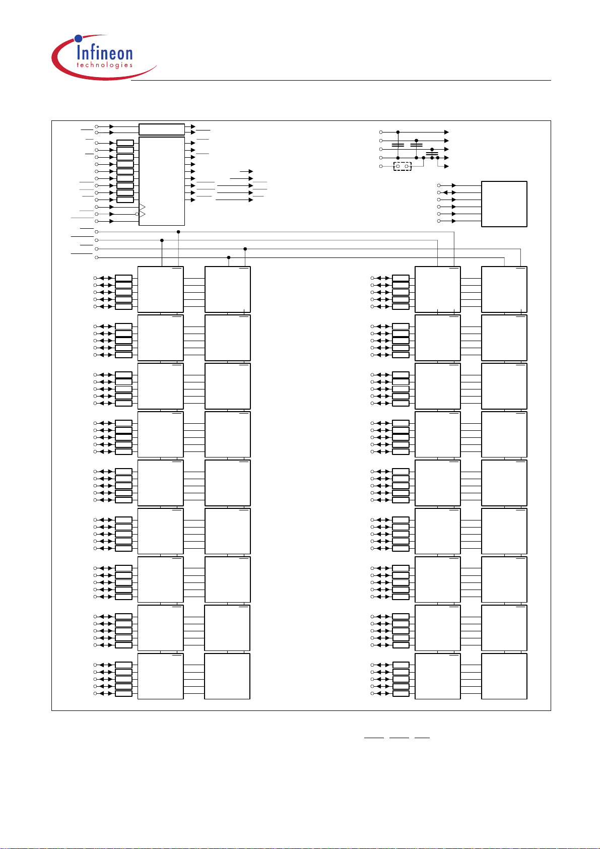
2 Pin Configuration
The pin configuration of the Registered DDR SDRAM
DIMM is listed by function in Table 3 (184 pins). The
abbreviations used in columns Pin and Buffer Type are
explained in Table 4 and Table 5 respectively. The pin
numbering is depicted in Figure 1.
Table 3 Pin Configuration of RDIMM
Pin# Name Pin
Type
Clock Signals
137 CK0 I SSTL Clock Signal
138 CK0
21 CKE0 I SSTL Clock Enable Rank 0
111 CKE1 I SSTL Clock Enable Rank 1
NC NC SSTL Note:1-rank module
Control Signals
157 S0
158 S1
NC NC – Note: 1-rank module
154 RAS
65 CAS
63 WE
10 RESET
Address Signals
59 BA0 I SSTL Bank Address Bus
52 BA1 I SSTL
48 A0 I SSTL Address Bus 11:0
43 A1 I SSTL
41 A2 I SSTL
130 A3 I SSTL
37 A4 I SSTL
32 A5 I SSTL Address Bus 11:0
I SSTL Complement Clock
I SSTL Chip Select of Rank 0
I SSTL Chip Select of Rank 1
I SSTL Row Address Strobe
I SSTL Column Address
I SSTL Write Enable
ILV-
Buffer
Type
CMOS
Function
Note: 2-rank module
Note: 2-ranks module
Strobe
Register Reset
Forces registered
inputs low
Note: For detailed
description of the
Power Up and
Power
Management see
the Application
Note at the end of
data sheet
1:0
Pin Configuration
Table 3 Pin Configuration of RDIMM (cont’d)
Pin# Name Pin
Type
125 A6 I SSTL Address Bus 11:0
29 A7 I SSTL
122 A8 I SSTL
27 A9 I SSTL
141 A10 I SSTL
AP I SSTL
118 A11 I SSTL
115 A12 I SSTL Address Signal 12
NC NC – Note: 128 Mbit based
167 A13 I SSTL Address Signal 13
NC NC – Note: Module based on
Buffer
Type
Function
Note: Module based on
256 Mbit or larger
dies
module
Note:1 Gbit based
module
512 Mbit or
smaller dies
Data Sheet 8 Rev. 1.0, 2004-03
HYS72D[128/64/32][300/320]GBR–[5/6]–C
Registered Double Data Rate SDRAM
Table 3 Pin Configuration of RDIMM (cont’d)
Pin# Name Pin
Type
Data Signals
2 DQ0 I/O SSTL Data Bus 63:0
4 DQ1 I/O SSTL
6 DQ2 I/O SSTL
8 DQ3 I/O SSTL
94 DQ4 I/O SSTL
95 DQ5 I/O SSTL
98 DQ6 I/O SSTL
99 DQ7 I/O SSTL
12 DQ8 I/O SSTL
13 DQ9 I/O SSTL
19 DQ10 I/O SSTL
20 DQ11 I/O SSTL
105 DQ12 I/O SSTL
106 DQ13 I/O SSTL
109 DQ14 I/O SSTL
110 DQ15 I/O SSTL
23 DQ16 I/O SSTL
24 DQ17 I/O SSTL
28 DQ18 I/O SSTL
31 DQ19 I/O SSTL
114 DQ20 I/O SSTL
117 DQ21 I/O SSTL
121 DQ22 I/O SSTL
123 DQ23 I/O SSTL
33 DQ24 I/O SSTL
35 DQ25 I/O SSTL
39 DQ26 I/O SSTL
40 DQ27 I/O SSTL
126 DQ28 I/O SSTL
127 DQ29 I/O SSTL
131 DQ30 I/O SSTL
133 DQ31 I/O SSTL
53 DQ32 I/O SSTL
55 DQ33 I/O SSTL
57 DQ34 I/O SSTL
60 DQ35 I/O SSTL
146 DQ36 I/O SSTL
147 DQ37 I/O SSTL
Buffer
Type
Function
Pin Configuration
Table 3 Pin Configuration of RDIMM (cont’d)
Pin# Name Pin
Type
150 DQ38 I/O SSTL Data Bus 63:0
151 DQ39 I/O SSTL
61 DQ40 I/O SSTL
64 DQ41 I/O SSTL
68 DQ42 I/O SSTL
69 DQ43 I/O SSTL
153 DQ44 I/O SSTL
155 DQ45 I/O SSTL
161 DQ46 I/O SSTL
162 DQ47 I/O SSTL
72 DQ48 I/O SSTL
73 DQ49 I/O SSTL
79 DQ50 I/O SSTL
80 DQ51 I/O SSTL
165 DQ52 I/O SSTL
166 DQ53 I/O SSTL
170 DQ54 I/O SSTL
171 DQ55 I/O SSTL
83 DQ56 I/O SSTL
84 DQ57 I/O SSTL
87 DQ58 I/O SSTL
88 DQ59 I/O SSTL
174 DQ60 I/O SSTL
175 DQ61 I/O SSTL
178 DQ62 I/O SSTL
179 DQ63 I/O SSTL
44 CB0 I/O SSTL Check Bits 7:0
45 CB1 I/O SSTL
49 CB2 I/O SSTL
51 CB3 I/O SSTL
134 CB4 I/O SSTL
135 CB5 I/O SSTL
142 CB6 I/O SSTL
144 CB7 I/O SSTL
5 DQS0 I/O SSTL Data Strobes 8:0
14 DQS1 I/O SSTL
25 DQS2 I/O SSTL
36 DQS3 I/O SSTL
56 DQS4 I/O SSTL
67 DQS5 I/O SSTL
Buffer
Type
Function
Note: See block
diagram for
corresponding
DQ signals
Data Sheet 9 Rev. 1.0, 2004-03
HYS72D[128/64/32][300/320]GBR–[5/6]–C
Registered Double Data Rate SDRAM
Table 3 Pin Configuration of RDIMM (cont’d)
Pin# Name Pin
Type
78 DQS6 I/O SSTL Data Strobes 8:0
86 DQS7 I/O SSTL
47 DQS8 I/O SSTL
97 DM0 I SSTL Data Mask 0
DQS9 I/O SSTL Data Strobe 9
107 DM1 I SSTL Data Mask 1
DQS10 I/O SSTL Data Strobe 10
119 DM2 I SSTL Data Mask 2
DQS11 I/O SSTL Data Strobe 11
129 DM3 I SSTL Data Mask 3
DQS12 I/O SSTL Data Strobe 12
149 DM4 I SSTL Data Mask 4
DQS13 I/O SSTL Data Strobe 13
159 DM5 I SSTL Data Mask 5
DQS14 I/O SSTL Data Strobe 14
169 DM6 I SSTL Data Mask 6
DQS15 I/O SSTL Data Strobe 15
177 DM7 I SSTL Data Mask 7
DQS16 I/O SSTL Data Strobe 16
140 DM8 I SSTL Data Mask 8
DQS17 I/O SSTL Data Strobe 17
Buffer
Type
Function
Note:
×
8 based module
Note:
×
4 based module
Note:
×
8 based module
Note:
×
4 based module
Note:
×
8 based module
×
Note:
Note:
Note:
Note:
Note:
Note:
Note:
Note:
Note:
Note:
Note:
Note:
Note:
4 based module
×
8 based module
×
4 based module
×
8 based module
×
4 based module
×
8 based module
×
4 based module
×
8 based module
×
4 based module
×
8 based module
×
4 based module
×
8 based module
×
4 based module
Pin Configuration
Table 3 Pin Configuration of RDIMM (cont’d)
Pin# Name Pin
Type
EEPROM
92 SCL I CMOS Serial Bus Clock
91 SDA I/O OD Serial Bus Data
181 SA0 I CMOS Slave Address Select
182 SA1 I CMOS
183 SA2 I CMOS
Power Supplies
1
184
15,
22,
30,
54,
62,
77,
96,
104,
112,
128,
136,
143,
156,
164,
172,
180
7,
38,
46,
70,
85,
108,
120,
148,
168
V
REF
V
DDSPD
V
DDQ
V
DD
AI – I/O Reference Voltage
PWR – EEPROM Power
PWR – I/O Driver Power
PWR – Power Supply
Buffer
Type
Function
Bus 2:0
Supply
Supply
Data Sheet 10 Rev. 1.0, 2004-03
HYS72D[128/64/32][300/320]GBR–[5/6]–C
Registered Double Data Rate SDRAM
Table 3 Pin Configuration of RDIMM (cont’d)
Pin# Name Pin
Type
V
3,
11,
18,
26,
34,
42,
50,
58,
66,
74,
81,
89,
93,
100,
116,
124,
132,
139,
145,
152,
160,
176
Other Pins
82
9,
16,
17,
71,
75,
76,
90,
101,
102,
103,
113,
163,
173
SS
V
DDID
NC NC – Not connected
GND – Ground Plane
OODVDD Identification
Buffer
Type
Function
Note: Pin in tristate,
indicating V
and V
connected on
PCB
Pins not connected on
Infineon RDIMM’s
DDQ
DD
nets
Pin Configuration
Table 4 Abbreviations for Pin Type
Abbreviation Description
I Standard input-only pin. Digital levels.
O Output. Digital levels.
I/O I/O is a bidirectional input/output signal.
AI Input. Analog levels.
PWR Power
GND Ground
NU Not Usable (JEDEC Standard)
NC Not Connected (JEDEC Standard)
Table 5 Abbreviations for Buffer Type
Abbreviation Description
SSTL Serial Stub Terminalted Logic (SSTL2)
LV-CMOS Low Voltage CMOS
CMOS
OD Open Drain. The corresponding pin has 2
CMOS Levels
operational states, active low and tristate,
and allows multiple devices to share as a
wire-OR.
Data Sheet 11 Rev. 1.0, 2004-03
HYS72D[128/64/32][300/320]GBR–[5/6]–C
Registered Double Data Rate SDRAM
V
REF
DQS0
NC
DQ09
NC
CKE0
DQS2
A7
DQ24
A4
A2
CB01
CB02
DQ32
DQ34
DQ40
CAS
DQ43
DQ49
V
DDQ
V
V
V
V
DM00/DQS9
NC
DQ12
DQ14
NC
DQ21
DQ22
A6
DM3/DQS12
DQ31
CK0
A10/AP
V
DM4/DQS13
DQ44
S0
DQ46
DQ52
DM6/DQS15
NC
DM7/DQS16
SA0
SS
DD
SS
SS
SS
Pin 001
Pin 005
Pin 009
Pin 013
Pin 017
Pin 021
Pin 025
Pin 029
Pin 033
Pin 037
-
-
Pin 041
-
Pin 045
-
Pin 049
-
Pin 053
-
Pin 057
-
Pin 061
-
Pin 065
-
Pin 069
-
Pin 073
-
Pin 077
-
Pin 081
-
Pin 085
-
Pin 089
-
Pin 093
-
Pin 097
-
Pin 101
-
Pin 105
-
Pin 109
-
Pin 113
-
Pin 117
-
Pin 121
-
Pin 125
-
Pin 129
-
Pin 133
-
Pin 137
-
Pin 141
-
Pin 145
-
Pin 149
-
Pin 153
-
Pin 157
-
Pin 161
-
Pin 165
-
Pin 169
-
Pin 173
-
Pin 177
-
Pin 181
V
V
V
V
DDQ
DQ10
DQ16
A9
DQ19
DQ25
DQ26
A1
DQS8
CB03
DQ33
BA0
WE
DQS5
NC
NC
DQ50
DQ56
DQ58
SDA
DQ05
DQ07
NC
DM1/DQS10
CKE1/NC
A12/NC
DM2/DQS11
DQ23
DQ29
DQ30
CB5
V
V
DDQ
DQ37
DQ39
DQ45
DM5/DQS14
NC
A13/NC
DQ55
DQ61
DQ63
SA2
SS
DD
SS
SS
Pin 003
Pin 007
Pin 011
Pin 015
Pin 019
Pin 023
Pin 027
Pin 031
Pin 035
Pin 039
-
Pin 043
Pin 047
Pin 051
Pin 055
Pin 059
Pin 063
Pin 067
Pin 071
Pin 075
Pin 079
Pin 083
Pin 087
Pin 091
Pin 095
Pin 099
Pin 103
Pin 107
Pin 111
Pin 115
Pin 119
Pin 123
Pin 127
Pin 131
Pin 135
Pin 139
Pin 143
Pin 147
Pin 151
Pin 155
Pin 159
Pin 163
Pin 167
Pin 171
Pin 175
Pin 179
Pin 183
-
Pin Configuration
Pin 002
-
Pin 004
Pin 008
Pin 012
Pin 016
Pin 020
Pin 024
Pin 028
Pin 032
Pin 036
Pin 040
Pin 044
Pin 048
Pin 052
Pin 056
FRONTSIDE
BACKSIDE
Pin 060
Pin 064
Pin 068
Pin 072
Pin 076
Pin 080
Pin 084
Pin 088
Pin 092
Pin 096
Pin 100
Pin 104
Pin 108
Pin 112
Pin 116
Pin 120
Pin 124
Pin 128
Pin 132
Pin 136
Pin 140
Pin 144
Pin 148
Pin 152
Pin 156
Pin 160
Pin 164
Pin 168
Pin 172
Pin 176
Pin 180
Pin 184
DQ01
DQ03
DQ08
NC
DQ11
DQ17
DQ18
A5
DQS3
DQ27
-
-
CB00
-
A0
-
BA1
-
DQS4
-
DQ35
-
DQ41
-
DQ42
-
DQ48
-
NC
-
DQ51
-
DQ57
-
DQ59
-
SCL
V
-
DDQ
V
-
SS
V
-
DDQ
V
-
DD
V
-
DDQ
V
-
SS
V
-
DD
V
-
SS
V
-
DDQ
V
-
SS
V
-
DDQ
-
DM8/DQS17
-
CB07
V
-
DD
V
-
SS
V
-
DDQ
V
-
SS
V
-
DDQ
V
-
DD
V
-
DDQ
V
-
SS
V
-
DDQ
-
V
DDSPD
Pin 006
Pin 010
Pin 014
Pin 018
Pin 022
Pin 026
Pin 030
Pin 034
Pin 038
Pin 042
Pin 046
Pin 050
Pin 054
Pin 058
Pin 062
Pin 066
Pin 070
Pin 074
Pin 078
Pin 082
Pin 086
Pin 090
Pin 094
Pin 098
Pin 102
Pin 106
Pin 110
Pin 114
Pin 118
Pin 122
Pin 126
Pin 130
Pin 134
Pin 138
Pin 142
Pin 146
Pin 150
Pin 154
Pin 158
Pin 162
Pin 166
Pin 170
Pin 174
Pin 178
Pin 182
DQ00
-
DQ02
-
RESET
-
DQS1
-
V
V
-
-
V
V
V
V
-
V
V
-
-
V
-
V
V
V
-
-
V
V
-
-
V
DQS6
-
V
DQS7
NC
DQ04
DQ06
NC
DQ13
DQ15
DQ20
A11
A8
DQ28
A3
DQ04
CK0
CB06
DQ36
DQ38
RAS
S1 /NC
DQ47
DQ53
DQ54
DQ60
DQ62
SA1
-
SS
DDQ
SS
DDQ
SS
DD
SS
DD
SS
DDQ
SS
DDQ
SS
DD
SS
DDID
MPPD0020
Figure 1 Pin Configuration 184 Pins, Reg
Table 6 Address Table
Density Organization Memory
Ranks
SDRAMs # of SDRAMs # of row/rank/
columns bits
Refresh Period Interval
256 MB 32 M ×72 1 32 M ×8 9 13 / 2 / 10 8K 64ms 7.8 µs
512 MB 64 M ×72 1 64 M ×4 18 13 / 2 / 11 8K 64ms 7.8 µs
Data Sheet 12 Rev. 1.0, 2004-03

HYS72D[128/64/32][300/320]GBR–[5/6]–C
Registered Double Data Rate SDRAM
Pin Configuration
Table 6 Address Table
Density Organization Memory
Ranks
SDRAMs # of SDRAMs # of row/rank/
columns bits
Refresh Period Interval
512 MB 64 M ×72 2 32 M ×8 18 13 / 2 / 10 8K 64ms 7.8 µs
1GB 128 M ×72 2 64 M ×4 36 13 / 2 / 11 8K 64ms 7.8 µs
CK0
CK0
S0
CKE0
BA0 - BA1
A0 - An
RAS
CAS
WE
PCK
PCK
RESET
S0
DM0/DQS9
DQS0
DQ0
DQ1
DQ2
DQ3
DQ4
DQ5
DQ6
DQ7
DM1/DQS10
DQS1
DQ8
DQ9
DQ10
DQ11
DQ12
DQ13
DQ14
DQ15
DM2/DQS11
DQS2
DQ16
DQ17
DQ18
DQ19
DQ20
DQ21
DQ22
DQ23
SCL
SAD
SA0
SA1
SA2
V
SS
PLL
R
E
G
I
S
T
E
R
DM CS
DQS
I/O 0
I/O 1
I/O 2
I/O 3
I/O 4
I/O 5
I/O 6
I/O 7
DM CS
DQS
I/O 0
I/O 1
I/O 2
I/O 3
I/O 4
I/O 5
I/O 6
I/O 7
DM CS
DQS
I/O 0
I/O 1
I/O 2
I/O 3
I/O 4
I/O 5
I/O 6
I/O 7
SCL
SAD
A0
A1
A2
WP
PCK
PCK
RS0
RCKE0
RBA0 - RBA1
RA0-RAn
RRAS
RCAS
RWE
D0
DM3/DQS12
D1
DM4/DQS13
D2
DM5/DQS14
E0
DQS3
DQ24
DQ25
DQ26
DQ27
DQ28
DQ29
DQ30
DQ31
DQS4
DQ32
DQ33
DQ34
DQ35
DQ36
DQ37
DQ38
DQ39
DQS5
DQ40
DQ41
DQ42
DQ43
DQ44
DQ45
DQ46
DQ47
VDD/V
CS: SDRAMs D0- D8
CKE: SDRAMs D0 - D8
BA0 - BA1: SDRAMs D0 - D8
A0 - An: SDRAMs D0 - D8
RAS: SDRAMs D0 - D8
CAS: SDRAMs D0 - D8
WE: SDRAMs D0 - D8
D3
D4
D5
VDD: SPD EEPROM E0
V
V
V
V
DD,SPD
V
V
DM CS
DQS
I/O 0
I/O 1
I/O 2
I/O 3
I/O 4
I/O 5
I/O 6
I/O 7
DM CS
DQS
I/O 0
I/O 1
I/O 2
I/O 3
I/O 4
I/O 5
I/O 6
I/O 7
DM CS
DQS
I/O 0
I/O 1
I/O 2
I/O 3
I/O 4
I/O 5
I/O 6
I/O 7
DDQ
REF
V
SS
DDID
Strap: see Note 1
DM6/DQS15
DQS6
DQ48
DQ49
DQ50
DQ51
DQ52
DQ53
DQ54
DQ55
DM7/DQS16
DQS7
DQ56
DQ57
DQ58
DQ59
DQ60
DQ61
DQ62
DQ63
DM8/DQS17
DQS8
CB0
CB1
CB2
CB3
CB4
CB5
CB6
CB7
DD/VDDQ
REF
SS
: SDRAMs D0 - D8
: SDRAMs D0 - D8
: SDRAMs D0 - D8
DM CS
DQS
I/O 0
I/O 1
I/O 2
I/O 3
I/O 4
I/O 5
I/O 6
I/O 7
DM CS
DQS
I/O 0
I/O 1
I/O 2
I/O 3
I/O 4
I/O 5
I/O 6
I/O 7
DM CS
DQS
I/O 0
I/O 1
I/O 2
I/O 3
I/O 4
I/O 5
I/O 6
I/O 7
MPBD1101
D6
D7
D8
Figure 2 Block Diagram Raw Card A ×72 1 Rank ×8, ECC
Notes
1.
V
DD
= V
, therefore V
DDQ
strap open
DDID
2. DQ, DQS, DM resistors are 22 ohms
±
5%
3. BAn, An, RAS
±
5%
, CAS, WE resistors are 22 ohms
Data Sheet 13 Rev. 1.0, 2004-03

HYS72D[128/64/32][300/320]GBR–[5/6]–C
Registered Double Data Rate SDRAM
BA0 - BA1
DM0/DQS9
DM1/DQS10
DM2/DQS11
DM3/DQS12
VDD/V
CK0
CK0
S0
CKE0
S1
CKE1
A0 - An
RAS
CAS
WE
PCK
PCK
RESET
S0
S1
DQS0
DQ0
DQ1
DQ2
DQ3
DQ4
DQ5
DQ6
DQ7
DQS1
DQ8
DQ9
DQ10
DQ11
DQ12
DQ13
DQ14
DQ15
DQS2
DQ16
DQ17
DQ18
DQ19
DQ20
DQ21
DQ22
DQ23
DQS3
DQ24
DQ25
DQ26
DQ27
DQ28
DQ29
DQ30
DQ31
V
DD,SPD
DDQ
V
REF
V
V
DDID
SS
Strap: see Note 1
PLL
R
E
G
I
S
T
E
R
CS
DM
DQS
I/O 0
I/O 1
I/O 2
I/O 3
I/O 4
I/O 5
I/O 6
I/O 7
CS
DM
DQS
I/O 0
I/O 1
I/O 2
I/O 3
I/O 4
I/O 5
I/O 6
I/O 7
CS
DM
DQS
I/O 0
I/O 1
I/O 2
I/O 3
I/O 4
I/O 5
I/O 6
I/O 7
CS
DM
DQS
I/O 0
I/O 1
I/O 2
I/O 3
I/O 4
I/O 5
I/O 6
I/O 7
VDD: SPD EEPROM E0
V
DD/VDDQ
V
REF
V
: SDRAMs D0 - D17
SS
DM: SDRAMs D0 - D17
PCK
PCK
RS0
RCKE0
RS1
RCKE1
RBA0 - RBA1
RA0 - RAn
RRAS
RCAS
RWE
D0
CS
DM
DQS
I/O 0
I/O 1
I/O 2
I/O 3
I/O 4
I/O 5
I/O 6
I/O 7
D1
CS
DM
DQS
I/O 0
I/O 1
I/O 2
I/O 3
I/O 4
I/O 5
I/O 6
I/O 7
D2
CS
DM
DQS
I/O 0
I/O 1
I/O 2
I/O 3
I/O 4
I/O 5
I/O 6
I/O 7
D3
CS
DM
DQS
I/O 0
I/O 1
I/O 2
I/O 3
I/O 4
I/O 5
I/O 6
I/O 7
: SDRAMs D0 - D17
: SDRAMs D0 - D17
CKE: SDRAMs D0 - D8
CKE: SDRAMs D9 - D17
BA0 - BA1: SDRAMs D0 - D17
A0 - An: SDRAMs D0 - D17
RAS: SDRAMs D0 - D17
CAS: SDRAMs D0 - D17
WE: SDRAMs D0 - D17
D9
D10
D11
D12
DM4/DQS13
DQS4
DQ32
DQ33
DQ34
DQ35
DQ36
DQ37
DQ38
DQ39
DM5/DQS14
DQS5
DQ40
DQ41
DQ42
DQ43
DQ44
DQ45
DQ46
DQ47
DM6/DQS15
DQS6
DQ48
DQ49
DQ50
DQ51
DQ52
DQ53
DQ54
DQ55
DM7/DQS16
DQS7
DQ56
DQ57
DQ58
DQ59
DQ60
DQ61
DQ62
DQ63
DM8/DQS17
DQS8
CB0
CB1
CB2
CB3
CB4
CB5
CB6
CB7
SCL
SAD
SA0
SA1
SA2
V
SS
CS
DM
DQS
I/O 0
I/O 1
I/O 2
I/O 3
I/O 4
I/O 5
I/O 6
I/O 7
CS
DM
DQS
I/O 0
I/O 1
I/O 2
I/O 3
I/O 4
I/O 5
I/O 6
I/O 7
CS
DM
DQS
I/O 0
I/O 1
I/O 2
I/O 3
I/O 4
I/O 5
I/O 6
I/O 7
CS
DM
DQS
I/O 0
I/O 1
I/O 2
I/O 3
I/O 4
I/O 5
I/O 6
I/O 7
CS
DM
DQS
I/O 0
I/O 1
I/O 2
I/O 3
I/O 4
I/O 5
I/O 6
I/O 7
Pin Configuration
E0
D13
D14
D15
D16
D17
D4
D5
D6
D7
D8
SCL
SAD
A0
A1
A2
WP
CS
DM
DQS
I/O 0
I/O 1
I/O 2
I/O 3
I/O 4
I/O 5
I/O 6
I/O 7
CS
DM
DQS
I/O 0
I/O 1
I/O 2
I/O 3
I/O 4
I/O 5
I/O 6
I/O 7
CS
DM
DQS
I/O 0
I/O 1
I/O 2
I/O 3
I/O 4
I/O 5
I/O 6
I/O 7
CS
DM
DQS
I/O 0
I/O 1
I/O 2
I/O 3
I/O 4
I/O 5
I/O 6
I/O 7
CS
DM
DQS
I/O 0
I/O 1
I/O 2
I/O 3
I/O 4
I/O 5
I/O 6
I/O 7
MPBD1401
Figure 3 Block Diagram Raw Card B ×72, 2Ranks ×8, ECC
Notes
1.
V
DD
= V
, therefore V
DDQ
strap open
DDID
2. DQ, DQS, DM resistors are 22 ohms ±5%
3. BAn, An, RAS
±5%
4. For Wire per Clock Loading please see Figure:
, CAS, WE resistors are 22 ohms
“Diferential Clock Net Wiring“
Data Sheet 14 Rev. 1.0, 2004-03

HYS72D[128/64/32][300/320]GBR–[5/6]–C
Registered Double Data Rate SDRAM
CK0
CK0
S0
CKE0
BA0 - BA1
A0 - An
RAS
CAS
WE
PCK
PCK
RESET
RS0
DQS0
DQ0
DQ1
DQ2
DQ3
DQS1
DQ8
DQ9
DQ10
DQ11
DQS2
DQ16
DQ17
DQ18
DQ19
DQS3
DQ24
DQ25
DQ26
DQ27
DQS4
DQ32
DQ33
DQ34
DQ35
DQS5
DQ40
DQ41
DQ42
DQ43
V
DD,SPD
VDD/V
DDQ
V
REF
V
V
DDID
SS
Strap: see Note 1
PLL
R
E
G
I
S
T
E
R
CS
DQS
I/O 0
I/O 1
I/O 2
I/O 3
CS
DQS
I/O 0
I/O 1
I/O 2
I/O 3
CS
DQS
I/O 0
I/O 1
I/O 2
I/O 3
CS
DQS
I/O 0
I/O 1
I/O 2
I/O 3
CS
DQS
I/O 0
I/O 1
I/O 2
I/O 3
CS
DQS
I/O 0
I/O 1
I/O 2
I/O 3
VDD: SPD EEPROM E0
V
V
V
PCK
PCK
RS0
RCKE0
RBA0 - RBA1
RA0 - RAn
RRAS
RCAS
RWE
D0
D1
D2
D3
D4
DQS10
D5
DQS11
DD/VDDQ
REF
SS
: SDRAMs D0 - D17
: SDRAMs D0 - D17
: SDRAMs D0 - D17
CS: SDRAMs D0- D17
CKE: SDRAMs D0 - D17
BA0 - BA1: SDRAMs D0 - D17
A0 - An: SDRAMs D0 - D17
RAS: SDRAMs D0 - D17
CAS: SDRAMs D0 - D17
WE: SDRAMs D0 - D17
DQS6
DQ48
DQ49
DQ50
DQ51
DQS7
DQ56
DQ57
DQ58
DQ59
DQS8
CB0
CB1
CB2
CB3
DQS9
DQ4
DQ5
DQ6
DQ7
DQ12
DQ13
DQ14
DQ15
DQ20
DQ21
DQ22
DQ23
CS
DQS
I/O 0
I/O 1
I/O 2
I/O 3
CS
DQS
I/O 0
I/O 1
I/O 2
I/O 3
CS
DQS
I/O 0
I/O 1
I/O 2
I/O 3
CS
DQS
I/O 0
I/O 1
I/O 2
I/O 3
CS
DQS
I/O 0
I/O 1
I/O 2
I/O 3
CS
DQS
I/O 0
I/O 1
I/O 2
I/O 3
Figure 4 Block Diagram Raw Card C ×72 1 Rank ×4, ECC
D6
D7
D8
D9
D10
D11
DQS12
DQ28
DQ29
DQ30
DQ31
DQS13
DQ36
DQ37
DQ38
DQ39
DQS14
DQ44
DQ45
DQ46
DQ47
DQS15
DQ52
DQ53
DQ54
DQ55
DQS16
DQ60
DQ61
DQ62
DQ63
DQS17
CB4
CB5
CB6
CB7
SCL
SAD
SA0
SA1
SA2
V
SS
Pin Configuration
CS
DQS
I/O 0
I/O 1
I/O 2
I/O 3
CS
DQS
I/O 0
I/O 1
I/O 2
I/O 3
CS
DQS
I/O 0
I/O 1
I/O 2
I/O 3
CS
DQS
I/O 0
I/O 1
I/O 2
I/O 3
CS
DQS
I/O 0
I/O 1
I/O 2
I/O 3
CS
DQS
I/O 0
I/O 1
I/O 2
I/O 3
SCL
SAD
A0
A1
A2
WP
D12
D13
D14
D15
D16
D17
E0
MPBD1501
Notes
1.
V
DD
= V
, therefore V
DDQ
strap open
DDID
2. DQ, DQS, DM resistors are 22 ohms
±
5%
3. BAn, An, RAS
±
5%
, CAS, WE resistors are 22 ohms
Data Sheet 15 Rev. 1.0, 2004-03
HYS72D[128/64/32][300/320]GBR–[5/6]–C
Registered Double Data Rate SDRAM
CK0
CK0
S0
CKE0
S1
CKE1
BA0 - BA1
A0 - An
RAS
CAS
WE
PCK
PCK
RESET
RS0
RCKE0
RS1
RCKE1
DQS0
DQ0
DQ1
DQ2
DQ3
DQS1
DQ8
DQ9
DQ10
DQ11
DQS10
DQ12
DQ13
DQ14
DQ15
DQS9
DQ4
DQ5
DQ6
DQ7
DQS11
DQ20
DQ21
DQ22
DQ23
DQS2
DQ16
DQ17
DQ18
DQ19
DQS3
DQ24
DQ25
DQ26
DQ27
DQS17
CB4
CB5
CB6
CB7
DQS12
DQ28
DQ29
DQ30
DQ31
PLL
R
E
G
I
S
T
E
R
CKE CS
DQS
I/O 0
I/O 1
I/O 2
I/O 3
CKE CS
DQS
I/O 0
I/O 1
I/O 2
I/O 3
CKE CS
DQS
I/O 0
I/O 1
I/O 2
I/O 3
CKE CS
DQS
I/O 0
I/O 1
I/O 2
I/O 3
CKE CS
DQS
I/O 0
I/O 1
I/O 2
I/O 3
CKE CS
DQS
I/O 0
I/O 1
I/O 2
I/O 3
CKE CS
DQS
I/O 0
I/O 1
I/O 2
I/O 3
CKE CS
DQS
I/O 0
I/O 1
I/O 2
I/O 3
CKE CS
DQS
I/O 0
I/O 1
I/O 2
I/O 3
PCK
PCK
RS0
RCKE0
RS1
RCKE1
RBA0 - RBA1
RA0-RAn
RRAS
RCAS
RWE
D4
CKE CS
DQS
I/O 0
I/O 1
I/O 2
I/O 3
D0
CKE CS
DQS
I/O 0
I/O 1
I/O 2
I/O 3
D12 D14
CKE CS
DQS
I/O 0
I/O 1
I/O 2
I/O 3
D8 D10
CKE CS
DQS
I/O 0
I/O 1
I/O 2
I/O 3
D20
CKE CS
DQS
I/O 0
I/O 1
I/O 2
I/O 3
D16 D18
CKE CS
DQS
I/O 0
I/O 1
I/O 2
I/O 3
D24
CKE CS
DQS
I/O 0
I/O 1
I/O 2
I/O 3
D28
CKE CS
DQS
I/O 0
I/O 1
I/O 2
I/O 3
D32
CKE CS
DQS
I/O 0
I/O 1
I/O 2
I/O 3
BA0 - BA1: SDRAMs D0 - D35
A0 - An: SDRAMs D0 - D35
RAS: SDRAMs D0 - D35
CAS: SDRAMs D0 - D35
WE: SDRAMs D0 - D35
D6
D2
D22
D26
D30
D34
Figure 5 Block Diagram Raw Card D ×72 2 Ranks ×4, ECC
V
VDD/V
DQS7
DQ56
DQ57
DQ58
DQ59
DQS6
DQ48
DQ49
DQ50
DQ51
DQS15
DQ52
DQ53
DQ54
DQ55
DQS16
DQ60
DQ61
DQ62
DQ63
DQS14
DQ44
DQ45
DQ46
DQ47
DQS5
DQ40
DQ41
DQ42
DQ43
DQS4
DQ32
DQ33
DQ34
DQ35
DQS8
CB0
CB1
CB2
CB3
DQS13
DQ36
DQ37
DQ38
DQ39
DD,SPD
DDQ
V
REF
V
V
DDID
SS
Strap: see Note 1
VDD: SPD EEPROM E0
V
V
V
DM: SDRAMs D0 - D35
SCL
SAD
SA0
SA1
SA2
V
SS
CKE CS
DQS
I/O 0
I/O 1
I/O 2
I/O 3
CKE CS
DQS
I/O 0
I/O 1
I/O 2
I/O 3
CKE CS
DQS
I/O 0
I/O 1
I/O 2
I/O 3
CKE CS
DQS
I/O 0
I/O 1
I/O 2
I/O 3
CKE CS
DQS
I/O 0
I/O 1
I/O 2
I/O 3
CKE CS
DQS
I/O 0
I/O 1
I/O 2
I/O 3
CKE CS
DQS
I/O 0
I/O 1
I/O 2
I/O 3
CKE CS
DQS
I/O 0
I/O 1
I/O 2
I/O 3
CKE CS
DQS
I/O 0
I/O 1
I/O 2
I/O 3
Pin Configuration
: SDRAMs D0 - D35
DD/VDDQ
: SDRAMs D0 - D35
REF
: SDRAMs D0 - D35
SS
SCL
SAD
A0
A1
A2
WP
D5
CKE CS
DQS
I/O 0
I/O 1
I/O 2
I/O 3
D1 D3
CKE CS
DQS
I/O 0
I/O 1
I/O 2
I/O 3
D13
CKE CS
DQS
I/O 0
I/O 1
I/O 2
I/O 3
D9
CKE CS
DQS
I/O 0
I/O 1
I/O 2
I/O 3
D21
CKE CS
DQS
I/O 0
I/O 1
I/O 2
I/O 3
D17
CKE CS
DQS
I/O 0
I/O 1
I/O 2
I/O 3
D25
CKE CS
DQS
I/O 0
I/O 1
I/O 2
I/O 3
D28 D31
CKE CS
DQS
I/O 0
I/O 1
I/O 2
I/O 3
D33
CKE CS
DQS
I/O 0
I/O 1
I/O 2
I/O 3
MPBD1061
E0
D7
D15
D11
D23
D19
D27
D35
Notes
1.
V
DD
= V
, therefore V
DDQ
strap open
DDID
2. DQ, DQS, DM resistors are 18 ohms
±
5%
3. BAn, An, RAS, CAS, WE resistors are 22 ohms ±5%
4. For Wire per Clock Loading please see Figure
“Differental Clock Net Wiring“
Data Sheet 16 Rev. 1.0, 2004-03

HYS72D[128/64/32][300/320]GBR–[5/6]–C
Registered Double Data Rate SDRAM
Electrical Characteristics
3 Electrical Characteristics
3.1 Operating Conditions
Table 7 Absolute Maximum Ratings
Parameter Symbol Values Unit Note/ Test
min. typ. max.
Voltage on I/O pins relative to
Voltage on inputs relative to
Voltage on
Voltage on
V
supply relative to V
DD
V
supply relative to V
DDQ
Operating temperature (ambient)
Storage temperature (plastic)
Power dissipation (per SDRAM component)
Short circuit output current
V
SS
V
SS
SS
SS
V
V
V
V
T
T
P
I
IN
IN
DD
DDQ
A
STG
D
OUT
, V
–0.5 – V
OUT
+0.5 V –
DDQ
–1 – +3.6 V –
–1 – +3.6 V –
–1 – +3.6 V –
0–+70°C–
-55 – +150 °C–
–1– W–
–50– mA–
Attention: Permanent damage to the device may occur if “Absolute Maximum Ratings” are exceeded. This
is a stress rating only, and functional operation should be restricted to recommended operation
conditions. Exposure to absolute maximum rating conditions for extended periods of time may
affect device reliability and exceeding only one of the values may cause irreversible damage to
the integrated circuit.
Condition
Table 8 Electrical Characteristics and DC Operating Conditions
Parameter Symbol Values Unit Note/Test Condition
Min. Typ. Max.
Device Supply Voltage
Device Supply Voltage
Output Supply Voltage V
Output Supply Voltage V
EEPROM supply voltage V
Supply Voltage, I/O Supply
Voltage
Input Reference Voltage
I/O Termination Voltage
V
DD
V
DD
DDQ
DDQ
DDSPD
V
SS
V
SSQ
V
REF
V
TT
2.3 2.5 2.7 V
f
≤ 166 MHz
CK
2.5 2.6 2.7 V fCK>166MHz
2.3 2.5 2.7 V f
≤ 166 MHz
CK
2.5 2.6 2.7 V fCK>166MHz
2.3 2.5 3.6 V —
,
00V—
0.49 × V
V
– 0.04 V
REF
DDQ
0.5 × V
DDQ
0.51 × V
+ 0.04 V
REF
DDQ
4)
V
5)
2)
3)
2)3)
(System)
Input High (Logic1) Voltage V
Input Low (Logic0) Voltage V
Input Voltage Level,
CK and CK
Inputs
Input Differential Voltage,
CK and CK
Inputs
VI-Matching Pull-up
V
V
VI
IH(DC)
IL(DC)
IN(DC)
ID(DC)
Ratio
V
+ 0.15 V
REF
–0.3 V
–0.3 V
0.36 V
+ 0.3 V
DDQ
– 0.15 V
REF
+ 0.3 V
DDQ
+ 0.6 V
DDQ
0.71 1.4 —
8)
8)
8)
8)6)
7)
Current to Pull-down
Current
1)
Data Sheet 17 Rev. 1.0, 2004-03
07302003-2MI6-FOP1
HYS72D[128/64/32][300/320]GBR–[5/6]–C
Registered Double Data Rate SDRAM
Electrical Characteristics
Table 8 Electrical Characteristics and DC Operating Conditions (cont’d)
Parameter Symbol Values Unit Note/Test Condition
1)
Min. Typ. Max.
Input Leakage Current
Output Leakage Current I
Output High Current,
I
I
OZ
I
OH
–2 2 µA Any input 0 V ≤ VIN≤ VDD;
All other pins not under test
8)9)
=0V
–5 5 µA DQs are disabled;
0V ≤
V
— –16.2 mA V
= 1.95 V
OUT
OUT
≤ V
DDQ
Normal Strength Driver
Output Low
I
OL
16.2 — mA V
= 0.35 V
OUT
Current, Normal Strength
Driver
1) 0 °C ≤ TA ≤ 70 °C
2) DDR400 conditions apply for all clock frequencies above 166 MHz
V
3) Under all conditions,
4) Peak to peak AC noise on
V
is not applied directly to the device. VTT is a system supply for signal termination resistors, is expected to be set equal
5)
TT
to V
, and must track variations in the DC level of V
REF
V
is the magnitude of the difference between the input level on CK and the input level on CK.
6)
ID
7) The ratio of the pull-up current to the pull-down current is specified for the same temperature and voltage, over the entire
temperature and voltage range, for device drain to source voltage from 0.25 to 1.0 V. For a given output, it represents the
maximum difference between pull-up and pull-down drivers due to process variation.
8) Inputs are not recognized as valid until
9) Values are shown per DDR SDRAM component
must be less than or equal to VDD.
DDQ
V
may not exceed ± 2% V
REF
V
stabilizes.
REF
REF (DC)
REF
. V
is also expected to track noise variations in V
REF
.
DDQ
.
Data Sheet 18 Rev. 1.0, 2004-03
07302003-2MI6-FOP1

HYS72D[128/64/32][300/320]GBR–[5/6]–C
Registered Double Data Rate SDRAM
Current Specification and Conditions
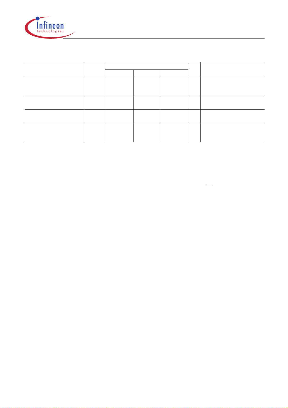
4 Current Specification and Conditions
Table 9 IDD Conditions
Parameter Symbol
Operating Current 0
one bank; active/ precharge; DQ, DM, and DQS inputs changing once per clock cycle;
address and control inputs changing once every two clock cycles.
Operating Current 1
one bank; active/read/precharge; Burst Length = 4; see component data sheet.
Precharge Power-Down Standby Current
all banks idle; power-down mode; CKE ≤
V
IL,MAX
Precharge Floating Standby Current
CS
≥ V
address and other control inputs changing once per clock cycle;
, all banks idle; CKE ≥ V
IH,,MIN
IH,MIN
;
V
IN
= V
for DQ, DQS and DM.
REF
Precharge Quiet Standby Current
CS
≥ V
address and other control inputs stable at ≥
, all banks idle; CKE ≥ V
IHMIN
IH,MIN
; VIN = V
V
IH,MIN
for DQ, DQS and DM;
REF
or ≤ V
IL,MAX
.
Active Power-Down Standby Current
one bank active; power-down mode; CKE ≤
V
ILMAX
; VIN = V
for DQ, DQS and DM.
REF
Active Standby Current
one bank active; CS
≥ V
IH,MIN
; CKE ≥ V
IH,MIN
; tRC= t
RAS,MAX
;
DQ, DM and DQS inputs changing twice per clock cycle;
address and control inputs changing once per clock cycle.
Operating Current Read
one bank active; Burst Length = 2; reads; continuous burst;
address and control inputs changing once per clock cycle;
50% of data outputs changing on every clock edge;
CL = 2 for DDR266(A), CL = 3 for DDR333 and DDR400B;
I
OUT
=0mA
Operating Current Write
one bank active; Burst Length = 2; writes; continuous burst;
address and control inputs changing once per clock cycle;
50% of data outputs changing on every clock edge;
CL = 2 for DDR266(A), CL = 3 for DDR333 and DDR400B
Auto-Refresh Current
t
RC
= t
RFCMIN
, burst refresh
Self-Refresh Current
CKE ≤ 0.2 V; external clock on
Operating Current 7
four bank interleaving with Burst Length = 4; see component data sheet.
I
DD0
I
DD1
I
DD2P
I
DD2F
I
DD2Q
I
DD3P
I
DD3N
I
DD4R
I
DD4W
I
DD5
I
DD6
I
DD7
Data Sheet 19 Rev. 1.0, 2004-03
07302003-2MI6-FOP1

HYS72D[128/64/32][300/320]GBR–[5/6]–C
Registered Double Data Rate SDRAM
Table 10
I
Specification for PC3200
DD
Current Specification and Conditions
Unit Note/ Test Conditions1)
HYS72D32300GBR–5–C
HYS72D64300GBR–5–C
HYS72D64320GBR–5–C
256 MB 512 MB 512 MB
×72 ×72 ×72
1 Rank 1 Rank 2 Ranks
Part Number & Organization
–5 –5 –5
Symbol Typ. Max. Typ. Max. Typ. Max.
I
DD0
I
DD1
I
DD2P
I
DD2F
I
DD2Q
I
DD3P
I
DD3N
I
DD4R
I
DD4W
I
DD5
I
DD6
I
DD7
1) Test condition for maximum values: VDD=2.7V, TA=10°C
2) Module
3) The module IDD values are calculated from the component IDD datasheet values are:
n * I
n * I
4) DQ I/O (I
conditions
5) The module IDD values are calculated from the component IDD datasheet values are:
n * I
2 * n * I
1510 1690 2140 2500 1852 2095 mA
1600 1780 2320 2680 1942 2185 mA
680 689 716 734 788 824mA
914 968 1184 1292 1184 1292 mA
824 896 1004 1148 1004 1148 mA
761 806 878 968 878 968mA
986 1049 1328 1454 1328 1454 mA
1645 1780 2410 2680 1987 2185 mA
1690 1825 2500 2770 2032 2230 mA
2140 2590 3400 4300 2482 2995 mA
657 670 669 694 669 694mA
2770 3130 4660 5380 3112 3535 mA
I
is calculated on the basis of component IDD and includes Register an PLL
DD
×[component] for single bank modules (n: number of components per module bank)
DD
×[component] + n * I
DD
) currents are not included into calculations: module IDD values will be measured differently depending on load
DDQ
×[component] for single bank modules (n: number of components per module bank)
DD
×[component] for single two bank modules (n: number of components per module bank)
DD
[component] for two bank modules (n: number of components per module bank)
DD3N
3)
3)4)
5)
5)
5)
5)
5)
3)4)
3)
3)
5)
3)4)
2)
Data Sheet 20 Rev. 1.0, 2004-03
07302003-2MI6-FOP1

HYS72D[128/64/32][300/320]GBR–[5/6]–C
Registered Double Data Rate SDRAM
Table 11
I
Specification for PC2700
DD
Current Specification and Conditions
Unit Note/ Test Conditions1)
HYS72D32300GBR–6–C
HYS72D64300GBR–6–C
HYS72D64320GBR–6–C
HYS72D128320GBR–6–C
256 MB 512 MB 512 MB 1 GB
×72 ×72 ×72 ×72
1 Rank 1 Rank 2 Ranks 2 Ranks
Part Number & Organization
–6 –6 –6 –6
Symbol Typ. Max. Typ. Max. Typ. Max. Typ. Max.
I
DD0
I
DD1
I
DD2P
I
DD2F
I
DD2Q
I
DD3P
I
DD3N
I
DD4R
I
DD4W
I
DD5
I
DD6
I
DD7
1) Test condition for maximum values: VDD=2.7V, TA=10°C
2) Module
3) The module IDD values are calculated from the component IDD datasheet values are:
n * I
n * I
4) DQ I/O (I
conditions
5) The module IDD values are calculated from the component IDD datasheet values are:
n * I
2 * n * I
1270 1405 1810 2080 1558 1747 2386 2764 mA
1360 1495 1990 2260 1648 1837 2566 2944 mA
466 475 502 520 574 610 718 790 mA
655 700 880 970 880 970 1330 1510 mA
583 646 736 862 736 862 1042 1294 mA
529 565 628 700 628 700 826 970 mA
718 772 1006 1114 1006 1114 1582 1798 mA
1360 1495 1990 2260 1648 1837 2566 2944 mA
1405 1540 2080 2350 1693 1882 2656 3034 mA
1810 2170 2890 3610 2098 2512 3466 4294 mA
443 455 455 480 455 480 480 531 mA
2350 2665 3970 4600 2638 3007 4546 5284 mA
I
is calculated on the basis of component IDD and includes Register an PLL
DD
×[component] for single bank modules (n: number of components per module bank)
DD
×[component] + n * I
DD
) currents are not included into calculations: module IDD values will be measured differently depending on load
DDQ
×[component] for single bank modules (n: number of components per module bank)
DD
×[component] for single two bank modules (n: number of components per module bank)
DD
[component] for two bank modules (n: number of components per module bank)
DD3N
2)
3)
3)4)
5)
5)
5)
5)
5)
3)4)
3)
3)
5)
3)4)
Data Sheet 21 Rev. 1.0, 2004-03
07302003-2MI6-FOP1

HYS72D[128/64/32][300/320]GBR–[5/6]–C
Registered Double Data Rate SDRAM
Current Specification and Conditions
4.1 AC Characteristics
Table 12 AC Timing - Absolute Specifications for PC3200 and PC2700
Parameter Symbol –5 –6 Unit Note/ Test
CK
CK
CK
ns
CK
CK
CK
CK
CK
CK
Condition
2)3)4)5)
2)3)4)5)
2)3)4)5)
2)3)4)5)
2)3)4)5)
2)3)4)5)
2)3)4)5)
2)3)4)5)
2)3)4)5)
2)3)4)5)
2)3)4)5)6)
2)3)4)5)6)
2)3)4)5)7)
2)3)4)5)7)
2)3)4)5)
2)3)4)5)
2)3)4)5)
2)3)4)5)
2)3)4)5)
2)3)4)5)
2)3)4)5)
2)3)4)5)
2)3)4)5)8)
2)3)4)5)9)
2)3)4)5)
3)4)5)6)10)
DQ output access time from CK/CK
DQS output access time from CK/CK t
CK high-level width t
CK low-level width t
Clock Half Period t
Clock cycle time t
DQ and DM input hold time t
DQ and DM input setup time t
Control and Addr. input pulse width (each
input)
DQ and DM input pulse width (each input) t
Data-out high-impedance time from CK/CK t
Data-out low-impedance time from CK/CK t
Write command to 1st DQS latching transition t
DQS-DQ skew (DQS and associated DQ
signals)
Data hold skew factor t
DQ/DQS output hold time t
DQS input low (high) pulse width (write cycle) t
DQS falling edge to CK setup time (write cycle) t
DQS falling edge hold time from CK (write
cycle)
Mode register set command cycle time t
Write preamble setup time t
Write postamble t
Write preamble t
Address and control input setup time t
t
AC
DQSCK
CH
CL
HP
CK
DH
DS
t
IPW
DIPW
HZ
LZ
DQSS
t
DQSQ
QHS
QH
DQSL,H
DSS
t
DSH
MRD
WPRES
WPST
WPRE
IS
DDR400B DDR333
Min. Max. Min. Max.
–0.5 +0.5 –0.7 +0.7 ns
–0.6 +0.6 –0.6 +0.6 ns
0.45 0.55 0.45 0.55 t
0.45 0.55 0.45 0.55 t
min. (tCL, tCH)min. (tCL, tCH)ns
5 8 6 12 ns CL = 3.0
6 12 6 12 ns CL = 2.5
7.5 12 7.5 12 ns CL = 2.0
0.4 — 0.45 — ns
0.4 — 0.45 — ns
2.2 — 2.2 — ns
1.75 — 1.75 — ns
— +0.7 –0.7 +0.7 ns
–0.7 +0.7 –0.7 +0.7 ns
0.72 1.25 0.75 1.25 t
— +0.40 — +0.40 ns TFBGA
— +0.50 — +0.50 ns TFBGA
t
–t
HP
QHS
0.35 — 0.35 — t
0.2 — 0.2 — t
0.2 — 0.2 — t
2—2—t
0—0—ns
0.40 0.60 0.40 0.60 t
0.25 — 0.25 — t
0.6 — 0.75 — ns fast slew rate
1)
Address and control input hold time t
0.7 — 0.8 — ns slow slew
IH
0.6 — 0.75 — ns fast slew rate
3)4)5)6)10)
rate
3)4)5)6)10)
0.7 — 0.8 — ns slow slew
3)4)5)6)10)
rate
Data Sheet 22 Rev. 1.0, 2004-03
07302003-2MI6-FOP1

HYS72D[128/64/32][300/320]GBR–[5/6]–C
Registered Double Data Rate SDRAM
Current Specification and Conditions
Table 12 AC Timing - Absolute Specifications for PC3200 and PC2700
Parameter Symbol –5 –6 Unit Note/ Test
DDR400B DDR333
Condition
1)
Min. Max. Min. Max.
Read preamble
Read postamble t
Active to Precharge command t
Active to Active/Auto-refresh command period t
Auto-refresh to Active/Auto-refresh command
t
RPRE
RPST
RAS
RC
t
RFC
0.9 1.1 0.9 1.1 t
0.40 0.60 0.40 0.60 t
40 70E+3 42 70E+3 ns
55 — 60 — ns
70 — 72 — ns
CK
CK
2)3)4)5)
2)3)4)5)
2)3)4)5)
2)3)4)5)
2)3)4)5)
period
ns
CK
2)3)4)5)
2)3)4)5)
2)3)4)5)
2)3)4)5)
2)3)4)5)
2)3)4)5)11)
Active to Read or Write delay t
Precharge command period t
Active to Autoprecharge delay t
Active bank A to Active bank B command t
Write recovery time t
Auto precharge write recovery + precharge
RCD
RP
RAP
RRD
WR
t
DAL
15 — 18 — ns
15 — 18 — ns
t
or t
RCD
RASmin
10 — 12 — ns
15 — 15 — ns
(tWR/tCK)+(tRP/tCK) t
time
Internal write to read command delay t
Exit self-refresh to non-read command t
Exit self-refresh to read command t
Average Periodic Refresh Interval t
1) 0 °C ≤ TA ≤ 70 °C; V
= 2.5 V ± 0.2 V, VDD = +2.5 V ± 0.2 V (DDR333); V
DDQ
WTR
XSNR
XSRD
REFI
2—1—t
75 — 75 — ns
200 — 200 — t
—7.8—7.8µs
= 2.6 V ± 0.1 V, VDD = +2.6 V ± 0.1 V
DDQ
(DDR400)
2) Input slew rate ≥ 1 V/ns for DDR400, DDR333
3) The CK/CK
level for signals other than CK/CK, is V
4) Inputs are not recognized as valid until
input reference level (for timing reference to CK/CK) is the point at which CK and CK cross: the input reference
. CK/CK slew rate are ≥ 1.0 V/ns.
REF
V
stabilizes.
REF
5) The Output timing reference level, as measured at the timing reference point indicated in AC Characteristics (note 3) is
6) These parameters guarantee device timing, but they are not necessarily tested on each device.
t
and tLZ transitions occur in the same access time windows as valid data transitions. These parameters are not referred
7)
HZ
to a specific voltage level, but specify when the device is no longer driving (HZ), or begins driving (LZ).
8) The specific requirement is that DQS be valid (HIGH, LOW, or some point on a valid transition) on or before this CK edge.
A valid transition is defined as monotonic and meeting the input slew rate specifications of the device. When no writes were
previously in progress on the bus, DQS will be transitioning from Hi-Z to logic LOW. If a previous write was in progress,
t
DQS could be HIGH, LOW, or transitioning from HIGH to LOW at this time, depending on
DQSS
.
9) The maximum limit for this parameter is not a device limit. The device operates with a greater value for this parameter, but
system performance (bus turnaround) degrades accordingly.
10) Fast slew rate ≥ 1.0 V/ns , slow slew rate ≥ 0.5 V/ns and < 1 V/ns for command/address and CK & CK
measured between
IH(ac)
and V
IL(ac)
.
V
11) For each of the terms, if not already an integer, round to the next highest integer. tCK is equal to the actual system clock
cycle time.
12) A maximum of eight Autorefresh commands can be posted to any given DDR SDRAM device.
2)3)4)5)
CK
2)3)4)5)
2)3)4)5)
CK
2)3)4)5)12)
V
slew rate > 1.0 V/ns,
TT
.
Data Sheet 23 Rev. 1.0, 2004-03
07302003-2MI6-FOP1

HYS72D[128/64/32][300/320]GBR–[5/6]–C
Registered Double Data Rate SDRAM
5SPD Contents
Table 13 SPD Codes for HYS72D[128/64/32][300/320]GBR–5–C
SPD Contents
HYS72D64300GBR–5–C
512 MB 512 MB 256 MB
×72 ×72 ×72
Product Type & Organization
Label Code PC3200R–30331 PC3200R–30331 PC3200R–30331
Jedec SPD Revision Rev 1.0 Rev 1.0 Rev 1.0
Byte# Description HEX HEX HEX
0 Programmed SPD Bytes in E2PROM 80 80 80
1 Total number of Bytes in E2PROM 08 08 08
2 Memory Type (DDR = 07h) 07 07 07
3 Number of Row Addresses 0D 0D 0D
4 Number of Column Addresses 0B 0A 0A
5 Number of DIMM Ranks 01 02 01
6 Data Width (LSB) 48 48 48
7 Data Width (MSB) 00 00 00
8 Interface Voltage Levels 04 04 04
9 tCK @ CLmax (Byte 18) [ns] 50 50 50
10 tAC SDRAM @ CLmax (Byte 18) [ns] 50 50 50
11 Error Correction Support 02 02 02
12 Refresh Rate 82 82 82
13 Primary SDRAM Width 04 08 08
14 Error Checking SDRAM Width 04 08 08
15 tCCD [cycles] 01 01 01
16 Burst Length Supported 0E 0E 0E
17 Number of Banks on SDRAM Device 04 04 04
18 CAS Latency 1C 1C 1C
19 CS Latency 01 01 01
20 Write Latency 02 02 02
21 DIMM Attributes 26 26 26
22 Component Attributes C1 C1 C1
23 tCK @ CLmax -0.5 (Byte 18) [ns] 60 60 60
24 tAC SDRAM @ CLmax -0.5 [ns] 50 50 50
25 tCK @ CLmax -1 (Byte 18) [ns] 75 75 75
1 Rank 2 Ranks 1 Rank
HYS72D64320GBR–5–C
HYS72D32300GBR–5–C
Data Sheet 24 Rev. 1.0, 2004-03
07302003-2MI6-FOP1

HYS72D[128/64/32][300/320]GBR–[5/6]–C
Registered Double Data Rate SDRAM
Table 13 SPD Codes for HYS72D[128/64/32][300/320]GBR–5–C
SPD Contents
HYS72D64300GBR–5–C
512 MB 512 MB 256 MB
×72 ×72 ×72
Product Type & Organization
Label Code PC3200R–30331 PC3200R–30331 PC3200R–30331
Jedec SPD Revision Rev 1.0 Rev 1.0 Rev 1.0
Byte# Description HEX HEX HEX
26 tAC SDRAM @ CLmax -1 [ns] 50 50 50
27 tRPmin [ns] 3C 3C 3C
28 tRRDmin [ns] 28 28 28
29 tRCDmin [ns] 3C 3C 3C
30 tRASmin [ns] 28 28 28
31 Module Density per Rank 80 40 40
32 tAS, tCS [ns] 60 60 60
33 tAH, TCH [ns] 60 60 60
34 tDS [ns] 40 40 40
35 tDH [ns] 40 40 40
36 - 40 not used 00 00 00
41 tRCmin [ns] 37 37 37
42 tRFCmin [ns] 41 41 41
43 tCKmax [ns] 28 28 28
44 tDQSQmax [ns] 28 28 28
45 tQHSmax [ns] 50 50 50
46 not used 00 00 00
47 DIMM PCB Height 01 01 01
48 - 61 not used 00 00 00
62 SPD Revision 10 10 10
63 Checksum of Byte 0-62 5F 27 26
64 JEDEC ID Code of Infineon (1) C1 C1 C1
65 - 71 JEDEC ID Code of Infineon (2 - 8) 00 00 00
72 Module Manufacturer Location xx xx xx
73 Part Number, Char 1 37 37 37
74 Part Number, Char 2 32 32 32
75 Part Number, Char 3 44 44 44
76 Part Number, Char 4 36 36 33
1 Rank 2 Ranks 1 Rank
HYS72D64320GBR–5–C
HYS72D32300GBR–5–C
Data Sheet 25 Rev. 1.0, 2004-03
07302003-2MI6-FOP1

HYS72D[128/64/32][300/320]GBR–[5/6]–C
Registered Double Data Rate SDRAM
Table 13 SPD Codes for HYS72D[128/64/32][300/320]GBR–5–C
SPD Contents
HYS72D64300GBR–5–C
512 MB 512 MB 256 MB
×72 ×72 ×72
Product Type & Organization
Label Code PC3200R–30331 PC3200R–30331 PC3200R–30331
Jedec SPD Revision Rev 1.0 Rev 1.0 Rev 1.0
Byte# Description HEX HEX HEX
77 Part Number, Char 5 34 34 32
78 Part Number, Char 6 33 33 33
79 Part Number, Char 7 30 32 30
80 Part Number, Char 8 30 30 30
81 Part Number, Char 9 47 47 47
82 Part Number, Char 10 42 42 42
83 Part Number, Char 11 52 52 52
84 Part Number, Char 12 35 35 35
85 Part Number, Char 13 43 43 43
86 Part Number, Char 14 20 20 20
87 Part Number, Char 15 20 20 20
88 Part Number, Char 16 20 20 20
89 Part Number, Char 17 20 20 20
90 Part Number, Char 18 20 20 20
91 Module Revision Code xx xx xx
92 Test Program Revision Code xx xx xx
93 Module Manufacturing Date Year xx xx xx
94 Module Manufacturing Date Week xx xx xx
95 - 98 Module Serial Number (1 - 4) xx xx xx
99 - 127 Blank FF FF FF
1 Rank 2 Ranks 1 Rank
HYS72D64320GBR–5–C
HYS72D32300GBR–5–C
Data Sheet 26 Rev. 1.0, 2004-03
07302003-2MI6-FOP1

HYS72D[128/64/32][300/320]GBR–[5/6]–C
Registered Double Data Rate SDRAM
Table 14 SPD Codes for HYS72D[128/64/32][300/320]GBR–6–C
SPD Contents
HYS72D128320GBR–6–C
1GByte 512MB 512MB 256MB
×72 ×72 ×72 ×72
Product Type & Organization
Label Code PC2700R–
Jedec SPD Revision Rev 0.0 Rev 0.0 Rev 0.0 Rev 0.0
Byte# Description HEX HEX HEX HEX
0 Programmed SPD Bytes in E2PROM 80 80 80 80
1 Total number of Bytes in E2PROM 08 08 08 08
2 Memory Type (DDR = 07h) 07 07 07 07
3 Number of Row Addresses 0D 0D 0D 0D
4 Number of Column Addresses 0B 0B 0A 0A
5 Number of DIMM Ranks 02 01 02 01
6 Data Width (LSB) 48 48 48 48
7 Data Width (MSB) 00 00 00 00
8 Interface Voltage Levels 04 04 04 04
9 tCK @ CLmax (Byte 18) [ns] 60 60 60 60
10 tAC SDRAM @ CLmax (Byte 18) [ns] 70 70 70 70
11 Error Correction Support 02 02 02 02
12 Refresh Rate 82 82 82 82
13 Primary SDRAM Width 04 04 08 08
14 Error Checking SDRAM Width 04 04 08 08
15 tCCD [cycles] 01 01 01 01
16 Burst Length Supported 0E 0E 0E 0E
17 Number of Banks on SDRAM Device 04 04 04 04
18 CAS Latency 0C 0C 0C 0C
19 CS Latency 01 01 01 01
20 Write Latency 02 02 02 02
21 DIMM Attributes 26 26 26 26
22 Component Attributes C1 C1 C1 C1
23 tCK @ CLmax -0.5 (Byte 18) [ns] 75 75 75 75
24 tAC SDRAM @ CLmax -0.5 [ns] 70 70 70 70
25 tCK @ CLmax -1 (Byte 18) [ns] 00 00 00 00
2 Ranks 1 Rank 2 Ranks 1 Rank
25330
HYS72D64300GBR–6–C
PC2700R–
25330
HYS72D64320GBR–6–C
PC2700R–
25330
HYS72D32300GBR–6–C
PC2700R–
25330
Data Sheet 27 Rev. 1.0, 2004-03
07302003-2MI6-FOP1

HYS72D[128/64/32][300/320]GBR–[5/6]–C
Registered Double Data Rate SDRAM
Table 14 SPD Codes for HYS72D[128/64/32][300/320]GBR–6–C
SPD Contents
HYS72D128320GBR–6–C
1 GByte 512 MB 512 MB 256 MB
×72 ×72 ×72 ×72
Product Type & Organization
Label Code PC2700R–
Jedec SPD Revision Rev 0.0 Rev 0.0 Rev 0.0 Rev 0.0
Byte# Description HEX HEX HEX HEX
26 tAC SDRAM @ CLmax -1 [ns] 00 00 00 00
27 tRPmin [ns] 48 48 48 48
28 tRRDmin [ns] 30 30 30 30
29 tRCDmin [ns] 48 48 48 48
30 tRASmin [ns] 2A 2A 2A 2A
31 Module Density per Rank 80 80 40 40
32 tAS, tCS [ns] 75 75 75 75
33 tAH, TCH [ns] 75 75 75 75
34 tDS [ns] 45 45 45 45
35 tDH [ns] 45 45 45 45
36 - 40 not used 00 00 00 00
41 tRCmin [ns] 3C 3C 3C 3C
42 tRFCmin [ns] 48 48 48 48
43 tCKmax [ns] 30 30 30 30
44 tDQSQmax [ns] 28 28 28 28
45 tQHSmax [ns] 50 50 50 50
46 not used 00 00 00 00
47 DIMM PCB Height 00 00 00 00
48 - 61 not used 00 00 00 00
62 SPD Revision 00 00 00 00
63 Checksum of Byte 0-62 49 48 10 0F
64 JEDEC ID Code of Infineon (1) C1 C1 C1 C1
65 - 71 JEDEC ID Code of Infineon (2 - 8) 00 00 00 00
72 Module Manufacturer Location xx xx xx xx
73 Part Number, Char 1 37 37 37 37
74 Part Number, Char 2 32 32 32 32
75 Part Number, Char 3 44 44 44 44
2 Ranks 1 Rank 2 Ranks 1 Rank
25330
HYS72D64300GBR–6–C
PC2700R–
25330
HYS72D64320GBR–6–C
PC2700R–
25330
HYS72D32300GBR–6–C
PC2700R–
25330
Data Sheet 28 Rev. 1.0, 2004-03
07302003-2MI6-FOP1

HYS72D[128/64/32][300/320]GBR–[5/6]–C
Registered Double Data Rate SDRAM
Table 14 SPD Codes for HYS72D[128/64/32][300/320]GBR–6–C
SPD Contents
HYS72D128320GBR–6–C
1GByte 512MB 512MB 256MB
×72 ×72 ×72 ×72
Product Type & Organization
Label Code PC2700R–
Jedec SPD Revision Rev 0.0 Rev 0.0 Rev 0.0 Rev 0.0
Byte# Description HEX HEX HEX HEX
76 Part Number, Char 4 31 36 36 33
77 Part Number, Char 5 32 34 34 32
78 Part Number, Char 6 38 33 33 33
79 Part Number, Char 7 33 30 32 30
80 Part Number, Char 8 32 30 30 30
81 Part Number, Char 9 30 47 47 47
82 Part Number, Char 10 47 42 42 42
83 Part Number, Char 11 42 52 52 52
84 Part Number, Char 12 52 36 36 36
85 Part Number, Char 13 36 43 43 43
86 Part Number, Char 14 43 20 20 20
87 Part Number, Char 15 20 20 20 20
88 Part Number, Char 16 20 20 20 20
89 Part Number, Char 17 20 20 20 20
90 Part Number, Char 18 20 20 20 20
91 Module Revision Code xx xx xx xx
92 Test Program Revision Code xx xx xx xx
93 Module Manufacturing Date Year xx xx xx xx
94 Module Manufacturing Date Week xx xx xx xx
95 - 98 Module Serial Number (1 - 4) xx xx xx xx
99 -127 Blank FF FF FF0 FF
2 Ranks 1 Rank 2 Ranks 1 Rank
25330
HYS72D64300GBR–6–C
PC2700R–
25330
HYS72D64320GBR–6–C
PC2700R–
25330
HYS72D32300GBR–6–C
PC2700R–
25330
Data Sheet 29 Rev. 1.0, 2004-03
07302003-2MI6-FOP1

HYS72D[128/64/32][300/320]GBR–[5/6]–C
Registered Double Data Rate SDRAM
6 Package Outlines
CA B
0.1
±0.1
4
1
±0.1
2.5
ø0.1
A
BC
64.77
133.35
128.95
6.62
2.175
Package Outlines
0.15
A
±0.13
28.58
92
6.35
49.53
B
0.4
BA C
2.64 MAX.
C
±0.1
1.27
±0.13
3.8
93
3 MIN.
Detail of contacts
0.2
1.27
1
±0.05
±0.2
2.5
95
x=120.65
1.27
1.8
0.1
A
CB
±0.1
0.1
BA
C
184
10
17.8
Burr max. 0.4 allowed
Figure 6 Package Outlines – Raw Card A HYS72D32300GBR–[5/6]–C (1 Rank × 8)
Data Sheet 30 Rev. 1.0, 2004-03
L-DIMM-184-021

HYS72D[128/64/32][300/320]GBR–[5/6]–C
Registered Double Data Rate SDRAM
±0.1
4
CB
A
0.1
1
2.5
±0.1
ø0.1
A BC
64.77
133.35
128.95
6.62
2.175
1.2795 x =
A
92
6.35
49.53
120.65
Package Outlines
0.15
±0.13
28.58
B
0.4
4 MAX.
C
1.27
BA C
±0.1
±0.13
3.8
93
3 MIN.
Detail of contacts
0.2
1.27
Burr max. 0.4 allowed
±0.05
1
±0.2
2.5
0.1
ABC
1.8
±0.1
0.1
AB
C
184
10
17.8
L-DIMM-184-22-2
Figure 7 Package Outlines – Raw Card C HYS72D64300GBR–[5/6]–C (1 Rank × 4)
Data Sheet 31 Rev. 1.0, 2004-03

HYS72D[128/64/32][300/320]GBR–[5/6]–C
Registered Double Data Rate SDRAM
6.62
x95
133.35
128.95
A
92
2.175
6.35
49.53
120.651.27 =
±0.1
4
B CA
0.1
1
2.5
±0.1
ø0.1
AB
64.77
C
Package Outlines
0.15
±0.13
28.58
B
C
0.4
4 MAX.
1.27
AB
±0.1
C
±0.13
3.8
93
3 MIN.
Detail of contacts
0.2
1.27
Burr max. 0.4 allowed
±0.05
±0.2
2.5
0.1
±0.1
1.8
C1B
A
0.1
BA
C
184
10
17.8
L-DIMM-184-23
Figure 8 Package Outlines – Raw Card B HYS72D64320GBR–[5/6]–C (2 Ranks ×8)
Data Sheet 32 Rev. 1.0, 2004-03

HYS72D[128/64/32][300/320]GBR–[5/6]–C
Registered Double Data Rate SDRAM
133.35
±0.1
4
BC
A
0.1
1
2.5
±0.1
ø0.1
ABC
64.77
128.95
6.62
2.175
1.27
95 x 120.65=
AA
92
6.35
49.53
Package Outlines
0.15
A BC
4 MAX.
±0.13
30.48
B
C
0.4
1.27
±0.1
±0.1
±0.13
3.8
93 184
3 MIN.
Detail of contacts
±0.2
1
2.5
±0.05
0.1
0.2
1.27
Burr max. 0.4 allowed
1.8
CA
B
0.1
A
CB
10
17.8
L-DIMM-184-24-3
Figure 9 Package Outlines – Raw Card D HYS72D128320GBR–[5/6]–C (2 Ranks ×4)
Data Sheet 33 Rev. 1.0, 2004-03

HYS72D[128/64/32][300/320]GBR–[5/6]–C
Registered Double Data Rate SDRAM
Application Note
7 Application Note
Power Up and Power Management on DDR Registered DIMMs (according to JEDEC ballot JC-42.5 Item
1173)
184-pin Double Data Rate (DDR) Registered DIMMs include two new features to facilitate controlled power-up and
to minimize power consumption during low power mode. One feature is externally controlled via a systemgenerated RESET signal; the second is based on module detection of the input clocks. These enhancements
permit the modules to power up with SDRAM outputs in a High-Z state (eliminating risk of high current dissipations
and/or dotted I/Os), and result in the powering-down of module support devices (registers and Phase-Locked
Loop) when the memory is in Self-Refresh mode.
The new RESET pin controls power dissipation on the module’s registers and ensures that CKE and other SDRAM
inputs are maintained at a valid ‘low’ level during power-up and self refresh. When RESET is at a low level, all the
register outputs are forced to a low level, and all differential register input receivers are powered down, resulting
in very low register power consumption. The RESET
an asynchronous signal according to the attached details. Using this function also permits the system and DIMM
clocks to be stopped during memory Self Refresh operation, while ensuring that the SDRAMs stay in Self Refresh
mode.
Table 15 RESET
Truth Table
pin, located on DIMM tab #10, is driven from the system as
Register Inputs Register
Outputs
RESET
H Rising Falling H H
H Rising Falling L L
H L or H L or H X Qo
H High Z High Z X Illegal input
L X or Hi-Z X or Hi-Z X or Hi-Z L
X: Don’t care, Hi-Z: High Impedance, Qo: Data latched at the previous of CK rising and CK
As described in the table above, a low on the RESET
maintained low at the SDRAM pins (CKE being one of the 'Q' signals at the register output). Holding CKE low
maintains a high impedance state on the SDRAM DQ, DQS and DM outputs — where they will remain until
activated by a valid ‘read’ cycle. CKE low also maintains SDRAMs in Self Refresh mode when applicable.
The DDR PLL devices automatically detect clock activity above 20MHz. When an input clock frequency of 20MHz
or greater is detected, the PLL begins operation and initiates clock frequency lock (the minimum operating
frequency at which all specifications will be met is 95MHz). If the clock input frequency drops below 20MHz (actual
detect frequency will vary by vendor), the PLL VCO (Voltage Controlled Oscillator) is stopped, outputs are made
High-Z, and the differential inputs are powered down — resulting in a total PLL current consumption of less than
1mA. Use of this low power PLL function makes the use of the PLL RESET
inactive on the DIMM.
This application note describes the required and optional system sequences associated with the DDR Registered
DIMM 'RESET
bank DIMM. Because RESET
CKE to one physical DIMM bank through the use of the RESET
' function. It is important to note that all references to CKE refer to both CKE0 and CKE1 for a 2-
CK CK Data in (D) Data out (Q)
applies to all DIMM register devices, it is therefore not possible to uniquely control
conditions
falling
input ensures that the Clock Enable (CKE) signal(s) are
(or G pin) unnecessary, and it is tied
pin.
Data Sheet 34 Rev. 1.0, 2004-03

HYS72D[128/64/32][300/320]GBR–[5/6]–C
Registered Double Data Rate SDRAM
Power-Up Sequence with RESET
1. The system sets RESET
This is the preferred default state during power-up. This input condition forces all register outputs to a low state
independent of the condition on the register inputs (data and clock), ensuring that CKE is at a stable low-level
at the DDR SDRAMs.
2. The power supplies should be initialized according to the JEDEC-approved initialization sequence for DDR
SDRAMs.
3. Stabilization of Clocks to the SDRAM
The system must drive clocks to the application frequency (PLL operation is not assured until the input clock
reaches 20 MHz). Stability of clocks at the SDRAMs will be affected by all applicable system clock devices,
and time must be allotted to permit all clock devices to settle. Once a stable clock is received at the DIMM PLL,
the required PLL stabilization time (assuming power to the DIMM is stable) is 100 microseconds. When a
stable clock is present at the SDRAM input (driven from the PLL), the DDR SDRAM requires 200 µsec prior to
SDRAM operation.
4. The system applies valid logic levels to the data inputs of the register (address and controls at the DIMM
connector).
CKE must be maintained low and all other inputs should be driven to a known state. In general these
commands can be determined by the system designer. One option is to apply an SDRAM ‘NOP’ command
(with CKE low), as this is the first command defined by the JEDEC initialization sequence (ideally this would
be a ‘NOP Deselect’ command). A second option is to apply low levels on all of the register inputs to be
consistent with the state of the register outputs.
5. The system switches RESET
The SDRAM is now functional and prepared to receive commands. Since the RESET
setting the RESET
must remain stable).
6. The system must maintain stable register inputs until normal register operation is attained.
The registers have an activation time that allows their clock receivers, data input receivers, and output drivers
sufficient time to be turned on and become stable. During this time the system must maintain the valid logic
levels described in step 5. It is also a functional requirement that the registers maintain a low state at the CKE
outputs to guarantee that the DDR SDRAMs continue to receive a low level on CKE. Register activation time
(
t (ACT) ), from asynchronous switching of RESET from low to high until the registers are stable and ready to
accept an input signal, is specified in the register and DIMM do-umentation.
7. The system can begin the JEDEC-defined DDR SDRAM power-up sequence (according to the JEDECpproved initialization sequence).
at a valid low level.
timing in relation to a specific clock edge is not required (during this period, register inputs
— Required
to a logic ‘high’ level.
Application Note
signal is asynchronous,
Self Refresh Entry (RESET
Self Refresh can be used to retain data in DDR SDRAM DIMMs even if the rest of the system is powered down
and the clocks are off. This mode allows the DDR SDRAMs on the DIMM to retain data without external clocking.
Self Refresh mode is an ideal time to utilize the RESET
(RESET
1. 1. The system applies Self Refresh entry command.
Note: Note: The commands reach the DDR SDRAM one clock later due to the additional register pipelining on a
2. The system sets RESET
3. The system turns off clock inputs to the DIMM. (Optional)
Data Sheet 35 Rev. 1.0, 2004-03
low deactivates register CK and CK, data input receivers, and data output drivers).
(CKE→Low, CS
Registered DIMM. After this command is issued to the SDRAM, all of the address and control and clock input
conditions to the SDRAM are Don’t Cares— with the exception of CKE.
This input condition forces all register outputs to a low state, independent of the condition on the registerm
inputs (data and clock), and ensures that CKE, and all other control and address signals, are a stable low-level
at the DDR SDRAMs. Since the RESET
specific clock edge is not required.
a. In order to reduce DIMM PLL current, the clock inputs to the DIMM are turned off, resulting in High-Z clock
→Low, RAS → Low, CAS→ Low, WE→ High)
low, clocks powered off) — Optional
pin, as this can reduce register power consumption
at a valid low level.
signal is asynchronous, setting the RESET timing in relation to a

HYS72D[128/64/32][300/320]GBR–[5/6]–C
Registered Double Data Rate SDRAM
inputs to both the SDRAMs and the registers. This must be done after the RESET
register (t (INACT). The deactivate time defines the time in which the clocks and the control and address
signals must maintain valid levels after RESET
documentation.
b.The system may release DIMM address and control inputs to High-Z.
This can be done after the RESET
the clocks and the control and the address signals must maintain valid levels after RESET
applied. It is highly recommended that CKE continue to remain low during this operation.
4. The DIMM is in lowest power Self Refresh mode.
Self Refresh Exit (RESET
1. Stabilization of Clocks to the SDRAM.
The system must drive clocks to the application frequency (PLL operation is not assured until the input clock
reaches ~20MHz). Stability of clocks at the SDRAMs will be affected by all applicable system clock devices,
and time must be allotted to permit all clock devices to settle. Once a stable clock is received at the DIMM PLL,
the required PLL stabilization time (assuming power to the DIMM is stable) is 100 microseconds.
2. The system applies valid logic levels to the data inputs of the register (address and controls at the DIMM
connector).
CKE must be maintained low and all other inputs should be driven to a known state. In general these
commands can be determined by the system designer. One option is to apply an SDRAM ‘NOP’ command
(with CKE low), as this is the first command defined by the JEDEC Self Refresh Exit sequence (ideally this
would be a ‘NOP Deselect’ command). A second option is to apply low levels on all of the register inputs, to
be consistent with the state of the register outputs.
3. The system switches RESET
The SDRAM is now functional and prepared to receive commands. Since the RESET
RESET
remain stable).
4. The system must maintain stable register inputs until normal register operation is attained.
The registers have an activation time that allows the clock receivers, input receivers, and output drivers
sufficient time to be turned on and become stable. During this time the system must maintain the valid logic
levels described in Step 2. It is also a functional requirement that the registers maintain a low state at the CKE
outputs to guarantee that the DDR SDRAMs continue to receive a low level on CKE. Register activation time
(t (ACT) ), from asynchronous switching of RESET
accept an input signal, is specified in the register and DIMM do-umentation.
5. System can begin the JEDEC-defined DDR SDRAM Self Refresh Exit Procedure.
timing relationship to a specific clock edge is not required (during this period, register inputs must
low, clocks powered off) — Optional
deactivate time of the register. The deactivate time defines the time in which
to a logic ‘high’ level.
low has been applied and is specified in the register and DIMM
from low to high until the registers are stable and ready to
Application Note
deactivate time of the
low has been
signal is asynchronous,
Self Refresh Entry (RESET
Although keeping the clocks running increases power consumption from the on-DIMM PLL during self refresh, this
is an alternate operating mode for these DIMMs.
1. 1. System enters Self Refresh entry command.
(CKE→ Low, CS
Note: Note: The commands reach the DDR SDRAM one clock later due to the additional register pipelining on a
Registered DIMM. After this command is issued to the SDRAM, all of the address and control and clock input
conditions to the SDRAM are Don’t Cares — with the exception of CKE.
2. The system sets RESET
This input condition forces all register outputs to a low state, independent of the condition on the data and clock
register inputs, and ensures that CKE is a stable low-level at the DDR SDRAMs.
3. The system may release DIMM address and control inputs to High-Z.
This can be done after the RESET
the time in which the clocks and the control and the address signals must maintain valid levels after RESET
low has been applied. It is highly recommended that CKE continue to remain low during the operation.
4. The DIMM is in a low power, Self Refresh mode.
Data Sheet 36 Rev. 1.0, 2004-03
→ Low, RAS→ Low, CAS→ Low, WE→ High)
low, clocks running) — Optional
at a valid low level.
deactivate time of the register (t (INACT) ). The deactivate time describes

HYS72D[128/64/32][300/320]GBR–[5/6]–C
Registered Double Data Rate SDRAM
Self Refresh Exit (RESET
1. The system applies valid logic levels to the data inputs of the register (address and controls at the DIMM
connector). CKE must be maintained low and all other inputs should be driven to a known state. In general
these commands can be determined by the system designer. One option is to apply an SDRAM ‘NOP’
command (with CKE low), as this is the first command defined by the Self Refresh Exit sequence (ideally this
would be a ‘NOP Deselect’ command). A second option is to apply low levels on all of the register inputs to be
consistent with the state of the register outputs.
2. The system switches RESET
The SDRAM is now functional and prepared to receive commands. Since the RESET
it does not need to be tied to a particular clock edge (during this period, register inputs must continue to remain
stable).
3. The system must maintain stable register inputs until normal register operation is attained.
The registers have an activation time that allows the clock receivers, input receivers, and output drivers
sufficient time to be turned on and become stable. During this time the system must maintain the valid logic
levels described in Step 1. It is also a functional requirement that the registers maintain a low state at the CKE
outputs in order to guarantee that the DDR SDRAMs continue to receive a low level on CKE. This activation
time, from asynchronous switching of RESET
an input signal, is t (ACT ) as specified in the register and DIMM documentation.
4. The system can begin JEDEC defined DDR SDRAM Self Refresh Exit Procedure.
Self Refresh Entry/Exit (RESET
As this sequence does not involve the use of the RESET
explains in detail the method for entering and exiting Self Refresh for this case.
low, clocks running) — Optional
to a logic 'high' level.
from low to high, until the registers are stable and ready to accept
high, clocks running) — Optional
function, the JEDEC standard SDRAM specification
Application Note
signal is asynchronous,
Self Refresh Entry (RESET
In order to maintain a valid low level on the register output, it is required that either the clocks be running and the
system drive a low level on CKE, or the clocks are powered off and RESET
sequence defined in this application note. In the case where RESET
the PLL drives a High-Z clock input into the register clock input. Without the low level on RESET
state will result.
high, clocks powered off) — Not Permissible
remains high and the clocks are powered off,
is asserted low according to the
an unknown DIMM
Data Sheet 37 Rev. 1.0, 2004-03

www.infineon.com
Published by Infineon Technologies AG
 Loading...