

Page 1

Application Note AN 2010-08
V2.0, August 2010
HybridPACK™ 2
General Information and Mounting Instruction
IFAG ATV OPEV
Page 2

2010-03
2009
Application Note AN 2010-08
V2.0,
Aug
ust 2010
Edition 2010-08-10
Published by
Infineon Technologies AG
59568 Warstein, Germany
© Infineon Technologies AG 2010.
All Rights Reserved.
Attention please!
THE INFORMATION GIVEN IN THIS APPLICATION NOTE IS GIVEN AS A HINT FOR THE
IMPLEMENTATION OF THE INFINEON TECHNOLOGIES COMPONENT ONLY AND SHALL NOT BE
REGARDED AS ANY DESCRIPTION OR WARRANTY OF A CERTAIN FUNCTIONALITY, CONDITION OR
QUALITY OF THE INFINEON TECHNOLOGIES COMPONENT. THE RECIPIENT OF THIS APPLICATION
NOTE MUST VERIFY ANY FUNCTION DESCRIBED HEREIN IN THE REAL APPLICATION. INFINEON
TECHNOLOGIES HEREBY DISCLAIMS ANY AND ALL WARRANTIES AND LIABILITIES OF ANY KIND
(INCLUDING WITHOUT LIMITATION WARRANTIES OF NON-INFRINGEMENT OF INTELLECTUAL
PROPERTY RIGHTS OF ANY THIRD PARTY) WITH RESPECT TO ANY AND ALL INFORMATION GIVEN
IN THIS APPLICATION NOTE.
Information
For further information on technology, delivery terms and conditions and prices please contact your nearest
Infineon Technologies Office (www.infineon.com).
Warnings
Due to technical requirements components may contain dangerous substances. For information on the types
in question please contact your nearest Infineon Technologies Office. Infineon Technologies Components
may only be used in life-support devices or systems with the express written approval of Infineon
Technologies, if a failure of such components can reasonably be expected to cause the failure of that life-
support device or system, or to affect the safety or effectiveness of that device or system. Life support
devices or systems are intended to be implanted in the human body, or to support and/or maintain and
sustain and/or protect human life. If they fail, it is reasonable to assume that the health of the user or other
persons may be endangered.
AN 2010-08
Revision History: date (10-08-10) V2.0, Previous Version: V1.0, November 2009
All Pages: Used new template. , Page 4 and 5: Added Chapter ” Proposal for Designing a Driver Board”
Page 7: Changed name of the JST connector from
"09HVD4B-EMGF-SR" to "09HVD6B-EMGF-NR".
Page 9: Added comment ”IFX does not
recommend the usage of a silicon gasket for sealing.”
Page 11: Changed drawing “
A design example of fluid cooling system”
Page 14: Updated
Figure 10
Author: Vase Klandjevski ( IFAG ATV OPEV AE )
We Listen to Your Comments
Any information within this document that you feel is wrong, unclear or missing at all? Your feedback will
help us to continuously improve the quality of this document. Please send your proposal (including a
reference to this document) to: [IGBT.Application@infineon.com]
Page 3

2010-03
2009
Application Note AN 2010-08
V2.0,
Aug
ust 2010
Table of Contents
1 Introduction ...................................................................................................................................4
2 Proposal for Designing a Driver Board ......................................................................................4
3 Mounting a Driver Board onto the Module .................................................................................6
4 Application of the Liquid Cooling System .................................................................................9
5 Screws to Mount the Module to the Heat Sink.........................................................................12
6 Mounting the Module to the Heat Sink .....................................................................................13
7 Connecting the Bus Bars to the Power Terminals ..................................................................14
7.1 Connecting the Power Terminals with Ideal Strain Relief ......................................................15
8 Storage and Transport ...............................................................................................................16
9 Data Matrix (DMX) Part Marking ................................................................................................17
Page 4

2010-03
2009
Application Note AN 2010-08
V2.0,
Aug
ust 2010
1 Introduction
The operation of high power modules results in power losses, which have to be dissipated
via a heat sink so that the maximum permissible temperature specified in the data sheet will
not be exceeded. Therefore, the mounting process of power modules is vital, because it
affects the module’s thermal performance and furthermore its reliability, which is critical for
automotive applications.
This application note gives mounting instructions for HybridPACK
TM
2 module with
recommendations how to screw the module, assemble the PCB and mount the module onto
the heat sink.
Please also note that ground straps should be worn while working with the components and
valid ESD safety instructions should be followed at all time, since IGBT modules are
electronic-static sensitive components. In addition, maximum permissible values in the
product datasheet and application notes are absolute limits which generally, even for short
times, may not be exceeded as this may lead to destruction of the component. Moreover, this
application note cannot cover every type of application and condition. Hence, the application
note cannot replace a detailed evaluation and examination by you or your technical divisions
of the suitability for the targeted applications. The application note will, therefore, under no
circumstances become part of any supplier agreed warranty, unless the supply agreement
determines otherwise in writing.
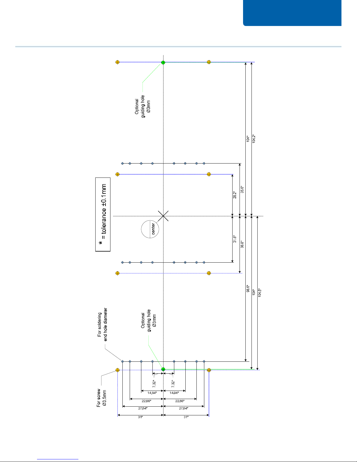
2 Proposal for Designing a Driver Board
Based on the HybridPACK™ 2 dimensions a proposal for designing a driver board can be
offered (see Figure 1). The end-hole diameter for the module solder pin connection should
be
0,0
25,0
35,1
−
+
mm should be taken.
PLEASE NOTE: The drawing below offers a proposal for solder pin connection based driver
board and therefore it is not binding. Detailed evaluation and examination by you or your
technical divisions must be done in order to verify the suitability of this proposal.
When designing a driver board which uses connectors (E.g. JST connector type "09HVD6BEMGF-NR") the geometry and the footprints of the connector must be taken in to account.
Page 5
2010-03
2009
Application Note AN 2010-08
V2.0,
Aug
ust 2010
mm
0,0
25,0
35,1
−
+
Figure 1 Proposal for designing a driver board for HybridPACK™ 2 module.
Page 6
2010-03
2009
Application Note AN 2010-08
V2.0,
Aug
ust 2010
3 Mounting a Driver Board onto the Module
The driver board could be mounted in two ways: through connectors (strongly
recommended) or alternative directly soldering on the top of the module.
When a driver board or module adapter board (PCB) is soldered directly on top of the
module, the contact joints (=solder connections) between PCB and module auxiliary contacts
should be mechanically relieved as much as possible. Relieve of the contact points is carried
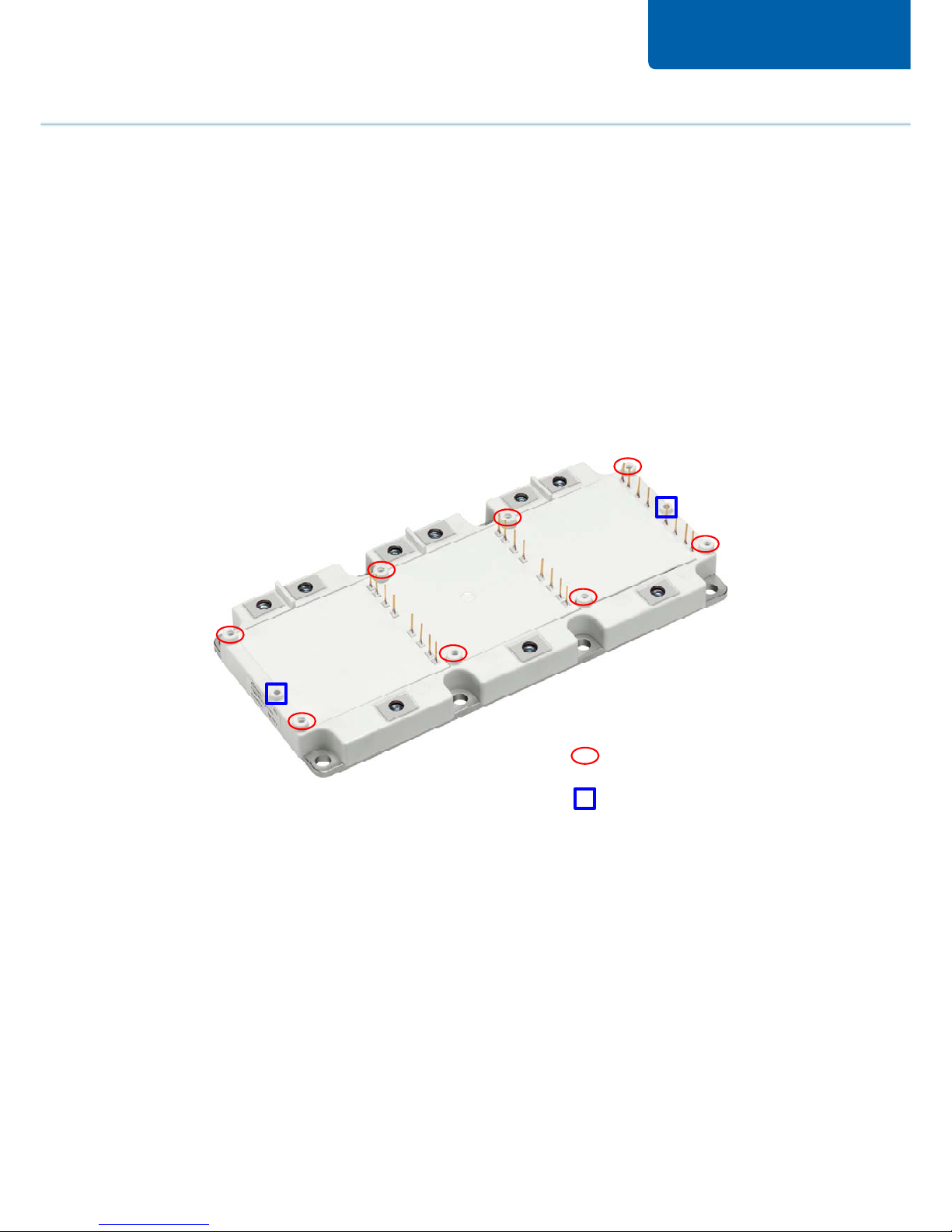
out by mounting the PCB directly onto the module at the eight mounting stand-offs (Figure 2)
using self-tapping (thread forming) screws or similar assembly material. The length of the
used self-tapping screws is depended on the PCB thickness. Example: For mounting a PCB
with 1.6mm thickness a self-trapping screw with 3 mm diameter and 10mm length should be
used for example type Delta PT 30x10 from EJOT.
Position of the mounting
„self-tapping“ screws
Position of the guidance
holes
1
2
3
4
5
6
7
8
Figure 2 PCB mounting stand-off of HybridPACK™ 2 module.
The screws should be mounted in the sequence showed in Figure 2. The initial 1.5mm of the
mounting stand-off serve as guidance only and cannot take any force. The thread in the
plastics will form itself by driving in the screws. Apart from manually driving the screws into
the mounting stand-offs an electronically controlled or at least slowly turning electric
screwdriver (≤300rpm) is a preferred aid (due to the lack of accuracy we do not recommend
the use of pneumatic screwdrivers). The maximum applied force M
max
is 0.9Nm ±10%. The
effective length of the screw thread entering the mounting stand-off should be of a minimum
length of l
min
≥6mm and a maximum length of l
max
≤9mm giving consideration to the PCB
thickness and the weight of the driver PCB.
Page 7

2010-03
2009
Application Note AN 2010-08
V2.0,
Aug
ust 2010
The HybridPACK™ 2 offers two guidance holes marked on the Figure 2 with the colour blue.
These guidance holes offer assistance by mounting the PCB on the module and allow
automated assembly.
To avoid damage or splitting of the stand-off, straight insertion of the screw into the stand-off
has to be observed during assembly (Figure 3).
A. Correctly assembled B. Incorrectly
positioned screw
Figure 3 (A) Correctly assembled screw into the mounting stand-off.
(B) Incorrectly positioned screw into the mounting stand-off.
The recommended screws and torques are based on laboratory tests. Depending on screws
and tools used, it may be necessary to adapt the assembly process accordingly.
After mounting the PCB the solder process (manual soldering, selective soldering or wave
soldering) may begin. When adhering to this sequence of assembly, the mechanical strain to
the solder points can be minimised.
During the entire soldering process care needs to be taken that neither a too high soldering
temperature nor a too long process time at the auxiliary pins overheats the plastic case and
thus deforms it.
According to IEC 68 section 2, a maximum solder temperature of T=260°C for a maximum
process time of t
max
≤10s has to be observed during the solder process.
Further information regarding solder processes can be referred to the application note
AN2005-06 “Soldering Econo und Easy modules”.
Instead of directly soldering, the PCB could also be mounted onto the module through
connectors. Such electrical connection between PCB and module can use every connector
which is designed for a pin cross-section of 0,64 x 0,64 mm, especially JST connector type
"09HVD6B-EMGF-NR". The module auxiliary terminals (pin connectors) are designed
especially for fitting to the JST connectors (surface and dimensions).
PCB
Modul
screw
PCB
Modul
screw
PCB
Modul
screw
PCB
Modul
screw
Modul
screw
Page 8

2010-03
2009
Application Note AN 2010-08
V2.0,
Aug
ust 2010
Figure 4 Technical drawing of the HybridPACKTM 2 auxiliary terminals (pin connectors).
The picture above shows the dimension and the structure of the auxiliary terminals. Due to
the specific requirements of the JST connector the auxiliary terminals have the following
properties:
• The auxiliary terminals are made of 63% IACS (International Annealed Copper
Standard) copper material,
• Auxiliary terminals have gold (Au) surface with nickel (Ni) under plating,
• The tensile strength of the auxiliary terminals has to be equal or exceed 530MPa,
Page 9

2010-03
2009
Application Note AN 2010-08
V2.0,
Aug
ust 2010
4 Application of the Liquid Cooling System
The power loss occurring in the module has to be dissipated in order not to exceed the
maximum permissible temperature specified in the datasheet during switching (T
vj_op
= 150
°C) in operation. Therefore, the design of cooling system/heat sink is of great importance to
achieve good performance.
HybridPACKTM 2 differs from other power modules because of pin-fin array on the base plate,
which makes liquid cooling very effective in sense of thermal performance. The base plate is
made of copper (Cu) material with nickel (Ni) plating. The pin fin structure is suitable for
cooling fluids like water/ethylenglycol mixture.
PLEASE NOTE: During the mounting process damages of the nickel plating and mechanical
deformation of the pin fin structure should be strictly avoided.
As shown in the figure below the pin-fin array is on the module base plate to get maximum
heat exchange effect. An O-ring sealing type (202 x 64.2 x 3 )mm e.g. from company
Trelleborg (part number
DRYD001590E768U) should be utilized on the heat sink in order to
confirm waterproof of the fluid cooling system. Such O-ring is held in a groove, which
surrounds the tray that holds the pin fin array, and this groove should be restricted to the
region on the heat sink that corresponds to the region around the pin fin structure see the
drawings below. With in this region there should be no contamination, scratches or other
base plate damages.
PLEASE NOTE:
IFX does not recommend the usage of a silicon gasket or other sealing
methods. The usage of sealing methods different then O-ring may cause damage on
HybridPACK™ 2 module.
Figure 5 Technical drawing of HybridPACK
TM
2 bottom side.
Page 10

2010-03
2009
Application Note AN 2010-08
V2.0,
Aug
ust 2010
Figure 6 “X”- section Detail drawing of the HybridPACK
TM
2 bottom side. The
sealing surface corresponds to the O-ring holding groove.
The suggested dimension of the tray holding the pin fin array is depicted in Figure 7a with
specified tolerances.
The contact surfaces between the base plate of the module and the surface of the heat sink
have to be free of degradation and contamination and should be cleaned with a fresh, lint
free cloth.
PLEASE NOTE: No thermal grease is needed for mounting the HybridPACK
TM
2 on the
cooler.
The contact surface of the heat sink should not exceed the following values referenced to a
length of L=100mm:
Surface flatness ≤50µm
Surface roughness Rz ≤10µm
Surface roughness at the sealing surface Ra ≤1.6µm
The heat sink has to be of sufficient stiffness for the assembly and the subsequent transport
in order not to exert additional straining or pulling forces to the base plate of the module.
During the entire assembly process the heat sink has to be handled twist free.
An example of fluid cooling system design could be referred to datasheet of HybridPACK
TM
2
and Figure 7. This cooling system is designed for O-ring sealing from Trelleborg with part
number
DRYD001590E768U.
Page 11

2010-03
2009
Application Note AN 2010-08
V2.0,
Aug
ust 2010
Figure 7 A design example of fluid cooling system.
Page 12

2010-03
2009
Application Note AN 2010-08
V2.0,
Aug
ust 2010
PLEASE NOTE. The heat sink design should be done in such manner in which the cooling
fluid has reduced bypass possibility.
The figure below presents the cross section view of HybridPACKTM 2 module and the heat
sink. This cross section shows that certain distances have to be minimized so that the
cooling fluid can not bypass the pin fin structure. One of the critical places is the border
region between the pin fin structure and the heat sink wall shown in the “A” area
(represented in the figure below with the black colour). If the distance between the pin fin
structure and the heat sink is too big it will offer unwilling path for the fluid. This will
eventually decrease the cooling performance. The second critical path is the gap between
the pin fin structure and the bottom of the heat sink (represented in the figure below with the
red colour). This gap should be minimized as well.
Figure 8 Cross section view of HybridPACKTM 2 and the heat sink. Within the shown
area “A” certain distances should be minimized in order to obtain
optimized cooling performance.
5 Screws to Mount the Module to the Heat Sink
To mount the module the following screws are recommended: DIN M6 screws which comply
at least with class 6.8 (for example, according to DIN 912 (ISO4762), ISO 7380, DIN 6912
and DIN 7984) in combination with a suitable dented edge washer and spring washer (for
example, according to DIN 433 or DIN 125) or the combination of both the “dented edge
washer”. The diameter of the used washer is 10mm.
The clearance and creepage distances specified in the HybridPACK™ 2 datasheets are the
shortest clearance and creepage distances existing at the unassembled and unconnected
module.
When selecting suitable M6 screws, washers and spring washers to mount the module, it is
recommended to consider the resulting clearance and creepage distances between the
power terminal and the nearest bolt head or washer during the development phase.
Page 13

2010-03
2009
Application Note AN 2010-08
V2.0,
Aug
ust 2010
6 Mounting the Module to the Heat Sink
The clamping force of the module resulting from the assembly process to the heat sink
depends on the torque applied and the condition of the heat sink material. The following
torque values specified in the datasheet result from steel screws in aluminium heat sinks with
a dry M6 thread and their typical friction factors of µ
G
=0.2~0.25 (µG=friction coefficient thread
in heat sink):
M
min
=3Nm to M
max
=6Nm.
For a good thermal contact to the heat sink the following procedure is recommended when
tightening the eight M6 fastening screws with washer (according to DIN 433) and spring
washer (according to DIN 127).
1. Place the module onto the heat sink and fix with two screws.
2. Fix the screws with 0.5Nm (hand tight crosswise) in the sequence showed in Figure 9.
3. Tighten the screws with 3Nm – 6Nm in the same sequence (crosswise)
Figure 9 Tightening sequence to mount the module.
Page 14

2010-03
2009
Application Note AN 2010-08
V2.0,
Aug
ust 2010
7 Connecting the Bus Bars to the Power Terminals
The DC power side should be connected with a laminated DC bus bar in order to keep the
switching overvoltage as low as possible by minimising the stray inductance. Adherence to
the maximum permissible voltage at the power terminals and at the IGBT chip is to be
assured according to the RBSOA data in the datasheet.
For the connection of the power terminals DIN M6 screws are required which comply at least
with class 6.8, in combination with a suitable washer and spring washer or complete
combination screws. These should be tightened with the recommended torque of M
min
=2.5
Nm to M
max
=5.0 Nm.
When selecting the screws length the layer thickness of the connected parts has to be
subtracted from the total length of the screws. The effective length of engagement into the
module thread may not exceed the maximum specified depth of 10mm.
The connected parts have to be mounted to the power terminals in such a way that the
specified static forces are not exceeded during assembly or later in operation, as shown in
Figure 10.
PLEASE NOTE: The values of the specified forces refer only to static forces. No oscillation
(swinging) forces are allowed here.
<100 N
<100 N
<100 N
<100 N
<100 N
200 N
Figure 10 Maximum permissible static pull and push forces at the power terminal
of the HybridPACK™ 2.
Page 15

2010-03
2009
Application Note AN 2010-08
V2.0,
Aug
ust 2010
7.1 Connecting the Power Terminals with Ideal Strain Relief
To connect the power terminals with the best possible strain relief, a recommended
assembly schematic is shown in Figure 11, in which a bus bar is connected to the power
terminals in such a way that only a low force is applied to them, even during shock or
vibration conditions. The power terminals can withstand the force F best in the direction from
the terminal to the base plate. Force to other directions has to be avoided. This has also to
be considered in the tolerance of the bus bar.
Figure 11 Concept drawing of HybridPACK™ 2 assembly with ideal strain relief
Page 16

2010-03
2009
Application Note AN 2010-08
V2.0,
Aug
ust 2010
8 Storage and Transport
Storage of the module at the temperature limitations specified in the datasheet is possible
but not recommended.
The recommended storage conditions according to IEC60721-3-1, class 1K2 should be
assured for the recommended storage time of max. 2 years.
Max. air temperature: T
maxair
=+40°C
Min. air temperature: T
minair
=+5°C
Max. relative humidity: 85%
Min. relative humidity: 5%
Condensation: not permissible
Precipitation: not permissible
Iceing: not permissible
Pre-drying of the case prior to the solder process, which is recommended for moulded
discrete components (e.g. microcontrollers, TO-cases etc.), is not required for HybridPACK™
2 modules
.
Page 17

2010-03
2009
Application Note AN 2010-08
V2.0,
Aug
ust 2010
9 Data Matrix (DMX) Part Marking
Infineon Technologies as a part of the electronic industry is making gains by using Data
Matrix part marking to transform the way of tracing HybridPACK
TM
products, both through the
manufacturing process, and throughout the entire life of that product or component. Total
traceability means dramatic improvements to process and quality control.
Data Matrix is a two-dimensional code which is machine readable with conventional 2D
reader or scanner. The readers are capable of reading low contrast marks, damaged codes
and even codes on severely compromised surfaces. On the picture below the side view of
HybridPACK
TM
2 is depicted. From this picture the marking of the module can be seen
together with the Data Matrix (DMX) - Code, Date Code and the Serial Nr.
Figure 12 HybridPACK™ 2 picture (side view)
When DMX-Code of the module depicted in above has been read out with a conventional
scanner, then the following characters will be shown:
Infineon Internal
tracking code
Serial Nr.
Date Code:
Year „09"
Calender Week „35"
Figure 13 HybridPACK™ 2 DMX Read-out
 Loading...