

Page 1

AN2017-44
1200V HighSpeed 3 IGBT in TO-247PLUS
Evaluation Board
User Manual
About this document
Scope and purpose
This application note is a user guide for the 1200V HighSpeed 3 IGBT in TO-247PLUS evaluation board.
It explains the board’s hardware and provides detailed instructions on how to use it for addressing
various measurement tasks. Finally, practical examples demonstrate the benefits of both, TO-247PLUS
and TO-247PLUS 4pin packages.
Intended audience
This document is intended for owners and users of the evaluation board.
Table of Contents
About this document .............................................................................................................................. 1
Table of Contents ................................................................................................................................... 1
1 Introduction .......................................................................................................................... 3
1.1 Purpose of the board .............................................................................................................. 3
1.2 Scope of delivery .................................................................................................................... 4
2 Hardware ............................................................................................................................... 5
2.1 Circuit and main components ................................................................................................. 5
2.2 Recommended accessories ................................................................................................... 6
3 Usage .................................................................................................................................... 8
3.1 Settings .................................................................................................................................. 8
3.1.1 Replacing switches or diodes ............................................................................................ 8
3.1.2 Changing between 3pin and 4pin packages ................................ ...................................... 9
3.1.3 Tuning gate voltages and resistors .................................................................................. 10
3.1.4 Adjusting and monitoring the heat sink temperature ........................................................ 11
3.2 Operation ............................................................................................................................. 11
3.2.1 Configurations ................................................................................................................. 11
3.2.2 Switching loss measurements ......................................................................................... 13
3.2.3 Efficiency or temperature measurements ......................................................................... 14
4 Examples ............................................................................................................................ 15
4.1 Turn-on loss reduction with a 4pin package ......................................................................... 15
4.2 Substituting parallel 40A devices with a 75A device ............................................................. 16
5 Appendix ............................................................................................................................. 18
5.1 Schematic drawing ............................................................................................................... 18
5.2 Board layout ......................................................................................................................... 19
5.3 Bill of materials ..................................................................................................................... 21
References ............................................................................................................................................ 24
Revision History ................................................................................................................................... 25
Application Note Please read the Important Notice and Warnings at the end of this document Revision 1.0
www.infineon.com 2017-11-15
Page 2

1200V HighSpeed 3 IGBT in TO-247PLUS Evaluation Board
User Manual
Introduction
Dangerous Equipment!
High Voltage
Do NOT touch the board during operation.
Depending on the configuration of the board and the chosen
supply-voltage, life-threatening voltages might be present!
Even brief accidental contact during operation
might result in severe injury or death!
Always make sure that the capacitors are discharged
before touching the board.
Only qualified personnel are allowed to handle this board!
Read the instructions provided in this application note before putting
the evaluation board into operation
The board described is an evaluation board dedicated for laboratory environment only. It operates at
high voltages and must only be operated by qualified and skilled personnel familiar with all applicable
safety standards.
Application Note 2 Revision 1.0
2017-11-15
Page 3
1200V HighSpeed 3 IGBT in TO-247PLUS Evaluation Board
User Manual
Introduction
(a)
(b)
1 Introduction
The evaluation board EVAL-IGBT-1200V-TO247PLUS was developed as a test platform for 1200V
IGBTs in TO-247PLUS and TO-247PLUS 4pin packages but can also be used for standard TO-247 and
TO-247 4pin packages.
This introductory section provides an overview of the potential applications of the evaluation board and
lists the components included in the delivery.
1.1 Purpose of the board
The main motivation to develop the evaluation board shown in Figure 1 was to have one universal test
platform for 1200V IGBTs in TO-247 as well as TO-247PLUS packages with three as well as four leads.
It allows evaluating the advantages provided by the larger lead frame area of the TO-247PLUS package
as well as the performance improvement given by the Kelvin emitter connection of the TO-247PLUS 4pin
package. For detailed information on these packages refer to application notes [1] and [2], respectively.
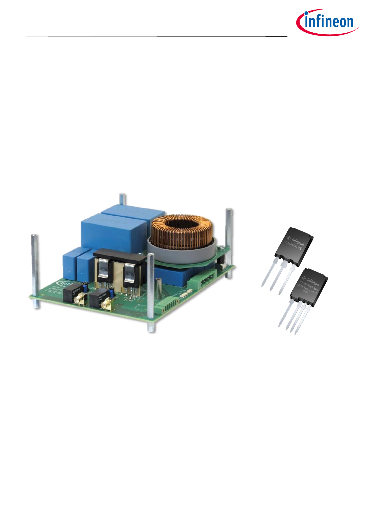
Figure 1 Evaluation board and devices under test: (a) 1200V HighSpeed 3 IGBT in TO-247PLUS
Evaluation Board, (b) TO-247PLUS and TO-247PLUS 4pin package
Two different modes of operation can be implemented with this board. First, it can be used to investigate
the switching behavior and measure the switching losses of IGBTs and diodes at different conditions.
Parameters like the DC link voltage, the load current, the device temperature as well as the gate
voltages and resistors are easily adjustable. If desired, snubbers can be assembled as well. Second, the
board can be operated as a step-up or step-down DC/DC converter. Thus, it is possible to characterize
and run devices in a continuous mode of operation in the same setup.
Care was taken to minimize the parasitic inductances and capacitances of this board wherever possible.
If needed, board users can tune the parasitic circuit elements by simply adding small capacitances and
inductances.
Application Note 3 Revision 1.0
2017-11-15
Page 4
1200V HighSpeed 3 IGBT in TO-247PLUS Evaluation Board
User Manual
Introduction
1.2 Scope of delivery
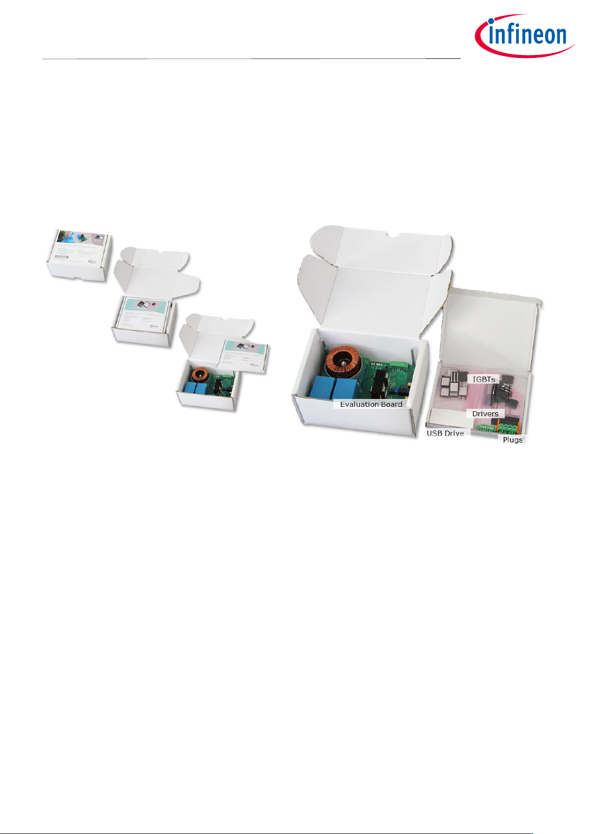
The evaluation board is delivered together with spare parts and complete documentation in an
environmentally friendly carton box as illustrated in Figure 2. As depicted, the carton box contains:
Evaluation board EVAL-IGBT-1200V-TO247PLUS with a size of 172mm x 133mm x 72mm (LxWxH)
1200V HighSpeed 3 IGBTs IKQ50N120CH3, IKQ75N120CH3, IKY50N120CH3 and IKY75N120CH3
1ED Compact isolated gate-driver ICs 1EDI60I12AH in a 300mil wide-body package
USB flash drive containing all related application notes and data sheets
Wire-to-board plugs for connecting the evaluation board to sources and loads
Figure 2 Scope of delivery: evaluation board, spare parts and USB drive with documentation
For high accuracy switching loss measurements, it is highly recommended to use these additional
components which are not included in the delivery:
Coaxial shunt SDN-414-xxx (IB Billmann) for high accuracy current measurements
Probe adapter A-PCB-5,0-L (PMK) for connecting a passive high voltage oscilloscope probe
Probe adapters PK106-4 (LeCroy) for connecting passive low voltage oscilloscope probes
Application Note 4 Revision 1.0
2017-11-15
Page 5

1200V HighSpeed 3 IGBT in TO-247PLUS Evaluation Board
User Manual
Hardware
(a)
(b)
2 Hardware
This section provides a short description of the board hardware. First, it explains the power circuitry, the
main components and the connectors. Then, the application of the recommended accessories is
discussed.
2.1 Circuit and main components
As shown in the block diagram of Figure 3, the evaluation board essentially is a half bridge converter
consisting of two IGBTs, S1 and S2. Due to the clip-based heat sink mounting and the universal socket
on the PCB it is possible to assemble standard TO-247 and TO-247PLUS packages with three as well
as four leads.
The switches are driven using EiceDriver™ 1ED Compact driver ICs. Due to the robust nature of the
coreless transformer technology combined with the 300mil wide-body package, these drivers are well
suited for applications that require high voltages, frequencies and switching speeds. Both drivers are
controlled with independent PWM signals on the connectors SIG-HS and SIG-LS. The driving voltages
are provided using the 12V auxiliary supply and isolated DC/DC converters.
For versatility reasons, the evaluation board was equipped with input and output capacitors Cin and C
out
as well as a load inductor L. While the input capacitor and the load inductor where designed having
mainly switching loss measurements in mind, the output capacitor is required for continuous operation,
for instance as a buck converter. The provided filter inductor might not meet the requirements for the
latter case but it is straightforward to replace it with a custom solution.
The same applies to the heat sink: its size and shape reveals that it cannot provide the cooling
performance required for continuous operation. Rather, it is intended to serve as a heating element for
performing high temperature switching loss measurements. Using the power resistor R
thermistor R
, the heat sink temperature can be adjusted and monitored, respectively. Again, it is
NTC
and the
POW
easily possible to replace the provided heat sink with a high performance solution.
Figure 3 Overview of the board schematics (a) and components (b)
Application Note 5 Revision 1.0
2017-11-15
Page 6

1200V HighSpeed 3 IGBT in TO-247PLUS Evaluation Board
User Manual
Hardware
(a)
(b)
An experimental analysis of a device’s switching behavior requires oscilloscope measurements of the
gate voltage, the collector-emitter voltage as well as the collector current. While voltage measurements
are straightforward, current measurements are more difficult to do, particularly in the presence of steep
current slopes. This evaluation board contains a basic SMD shunt resistor solution. It gives an
impression of the collector current waveform but is not considered an ideal solution for high accuracy
measurements.
2.2 Recommended accessories
The introductory section already clarified which components are delivered with the evaluation board and
which are not. Although the board can be used for switching loss measurements right away, it is strongly
recommended to use additional components for the highest accuracy and signal quality.
Coaxial shunt
Performing oscilloscope measurements of an IGBT’s collector current waveform is typically a non-trivial
task, particularly during switching events where extremely steep current slopes of several Amperes per
nanosecond are reached. An ideal current measurement for this purpose would be non-invasive – at
least it should not require significant changes of the circuit – and have a very high bandwidth.
By default, this evaluation board contains a 50mΩ metal foil SMD shunt resistor and an RC low-pass
filter in order to suppress disturbances caused by parasitic circuit elements. Due to the substantial
filtering, this approach might be considered a current estimation rather than a measurement. For high
accuracy measurements it is recommended to use a coaxial shunt SDN-414-xxx.[3] It has a bandwidth in
the gigahertz range and can be connected to any oscilloscope with a standard BNC cable.
To assemble the coaxial shunt:
1. Unsolder the 50mΩ metal foil resistor R201 and the 100Ω thin film resistor R200 on the bottom side
of the board.
2. Optionally, remove the capacitor C201 and the probe adapter Id2 as they are inoperable.
3. Strip the isolation at the central terminal of the shunt and solder it to the PCB.
As visible in Figure 4, the shunt should be positioned as close to the PCB as possible to minimize
parasitic inductances.
Figure 4 Recommended accessories for switching loss measurements: (a) pictures of the
components, (b) assembly of the components on the board
Application Note 6 Revision 1.0
2017-11-15
Page 7
1200V HighSpeed 3 IGBT in TO-247PLUS Evaluation Board
User Manual
Hardware
25°C
100°C
800V
400V
800V
400V
Turn-On
Turn-Off
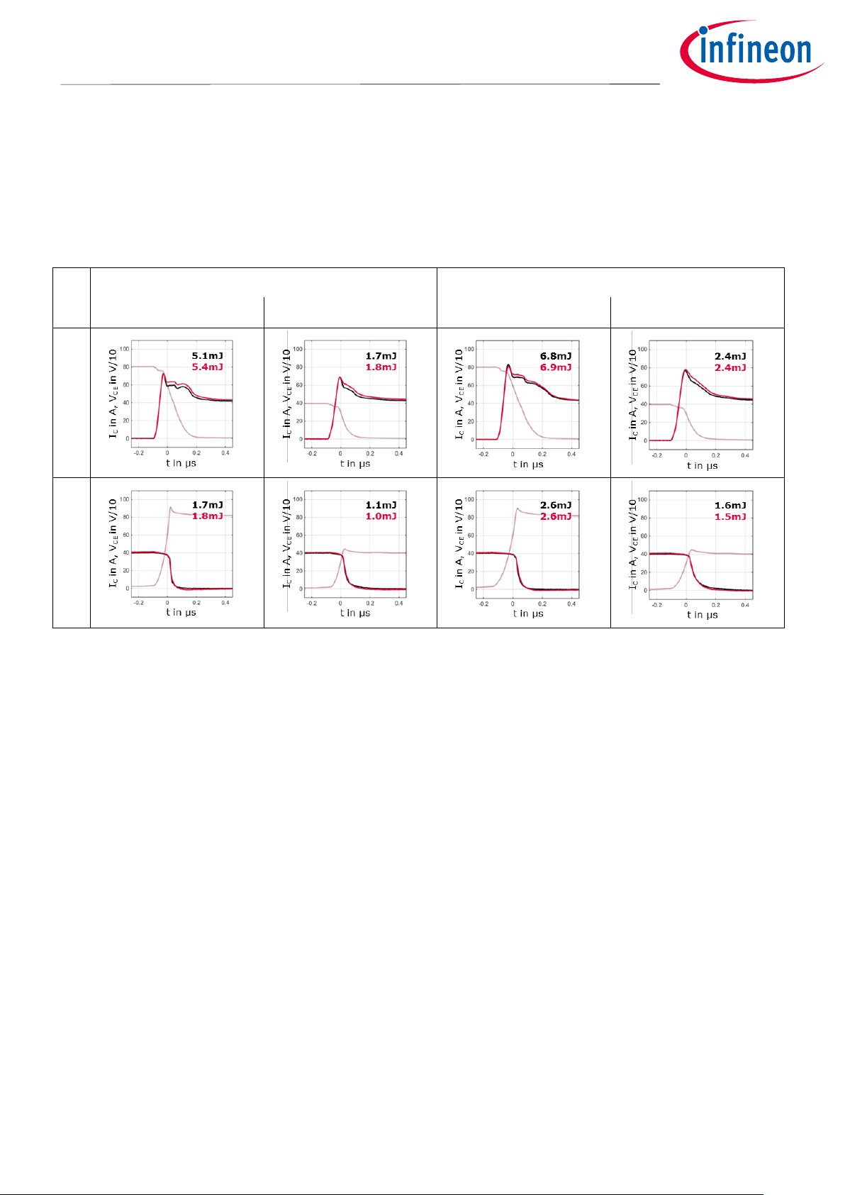
Table 1 compares waveforms as well as switching losses measured with the metal foil SMD resistor and
the coaxial shunt at various temperatures and voltages. As all measurements are done with exactly the
same semiconductor devices, the differences can be attributed to the different current sensors. It is
clearly visible that the SMD solution estimates the basic waveform of the collector current relatively well.
However, the exact determination of switching slopes and losses requires a coaxial shunt.
Table 1 Comparison of the coaxial (black) and the SMD shunt (red) at various conditions. The
double pulse tests were performed with IKY75N120CH3.
Oscilloscope probe adapters
In contrast to current measurements, the acquisition of voltage waveforms is straightforward. By
selecting the emitter potential of the low side IGBT S2 as common ground, the gate voltage, the collectoremitter voltage and the collector current can be measured with ordinary passive probes.
While voltage probes can be connected using grounding wires and clips, the use of PCB adapters is
considered advantageous for several reasons. First and foremost, the grounding of the probe is
improved which leads to a proper and reproducible signal quality, especially in the presence of
disturbances caused by switching transients. Additionally, connecting the probes becomes more
convenient and less error-prone.
The evaluation board was designed to accommodate one PMK high voltage probe adapter A-PCB-5,0-L
and two LeCroy low voltage probe adapters PK106-4 [4][5]. They share the emitter of the low-side switch
as common ground and measure the voltage on the collector, on the gate and on the Kelvin connection
terminal, respectively. Assembling the probe adapters can be done as depicted in Figure 4.b.
Application Note 7 Revision 1.0
2017-11-15
Page 8

1200V HighSpeed 3 IGBT in TO-247PLUS Evaluation Board
User Manual
Usage
(a)
(b)
(c)
(d)
3 Usage
Due to its flexibility, the evaluation board can address a variety of measurement problems. While the
previous sections explained the basic purpose as well as the hardware of the board, this section
provides detailed instructions on how to set it up and operate it. Section 3.1 describes how to modify
certain board settings, section 3.2 deals with the preparation and execution of different experiments.
3.1 Settings
The evaluation board is capable of testing TO-247 and TO-247PLUS packages with three as well as four
leads under many different conditions. This section provides exemplary instructions on how to assemble
different package variants and make the most important adjustments, particularly in the driving circuitry.
Attention: Prevent potential exposure to hazardous voltages by turning off all power supplies
and discharging the DC link capacitors before undertaking any of the modifications
described in the remainder of this section.
3.1.1 Replacing switches or diodes
A PCB is subject to severe thermomechanical stress when soldering and unsoldering components. As a
consequence, the adhesion between the copper layers and the core material gets weaker and
eventually, copper pads or traces may lift off and break. In order to allow a large number of IGBT and
diode replacements, this evaluation board uses press fit pins for connecting the TO packages and the
PCB. As the device is not soldered directly to the board but to the pins, the stress to the PCB is limited.
There are several ways of removing the TO packages from the heat sink and the board. A simple
approach is to cut the package leads, remove the package body from the heat sink and unsolder one
lead after another from the press fit pins. Figure 5 illustrates a different strategy where the
semiconductor device remains intact.
1. Put the board in an upright position so that the IGBT packages face upwards (a).
2. Push a flat screw driver between the clip and the package body and twist it to pull the clip out of the
heat sink’s groove (b).
3. Use two soldering irons to heat up all leads at the same time. When the solder melts on all leads,
gently pull the package away from the board (c).
4. Finally, clean the press fit pins using solder wick (d).
Figure 5 Disassembling a device from the heat sink and the PCB
The assembly of a new device is easier. Figure 6 presents a possible sequence of steps.
1. Prepare the TO package by cutting the leads to a length of around 5mm (a).
2. Place the package freely and perfectly flat on the heat sink (b).
3. Put the spring clip on the package and the heat sink groove and fasten it using pliers (c).
4. Solder one lead after the other to the press fit pins (d).
Application Note 8 Revision 1.0
2017-11-15
Page 9

1200V HighSpeed 3 IGBT in TO-247PLUS Evaluation Board
User Manual
Usage
(a)
(b)
(c)
(d)
Package
TO-247 4pin
TO-247PLUS 4pin
TO-247
TO-247PLUS
Connected
press fit pins
Pins 2-5
Pins 1-3
Reference of
driver output
Pin 3
(0Ω resistor at R2_4)
Pin 4
(0Ω resistor at R2_3)
Pin 3
(0Ω resistor at R2_4)
Pin 4
(0Ω resistor at R2_3)
Connection
Scheme
Picture
Comment
Operation of the
4pin package as a
3pin package
Intended operation
of the 4pin package
Intended operation
of the 3pin package
Attention: floating
gate; setting can
cause device and
circuit destruction
Figure 6 Assembling a device onto the heat sink and the PCB
3.1.2 Changing between 3pin and 4pin packages
Since the evaluation board has to serve as a universal test platform for TO-247-like packages with three
as well as four leads, it contains special five pin sockets which can accommodate all package variants.
The connection schemes for switches and drivers are described in Table 2.
1. Solder the discrete semiconductor package to the proper socket pins: four lead packages to pins 2-5,
three lead packages to pins 1-3.
2. Ensure that the reference of the driver output is connected to the proper Emitter lead using a 0Ω
resistor: assemble R214/R224 for a three-pin, R213/R223 for a four pin configuration.
Table 2 Assembly of TO-247-like packages with three and four pins
Application Note 9 Revision 1.0
2017-11-15
Page 10

1200V HighSpeed 3 IGBT in TO-247PLUS Evaluation Board
User Manual
Usage
(b)
(a)
(c)
3.1.3 Tuning gate voltages and resistors
Figure 7.a illustrates the schematics of the driving circuitry implemented for both, the high side and the
low side switch. It includes the relevant components of the circuitry and highlights the most important
part labels which consist of a letter and a three-digit number. The second digit is replaced by a wildcard
underscore in the picture but would normally indicate whether the component belongs to the high side
(“1”) or the low side (“2”).
A galvanically isolated EiceDriver™ 1ED Compact IC with a nominal current of 6A, separate source and
sink outputs and a wide-body package forms the core of the driving circuitry. The input or primary side of
the driver is powered with a voltage of 5V referring to SGND – this voltage is generated based on the
12V auxiliary input using a linear regulator – and controlled with a PWM signal on the input Sig-X. Please
note that since the driver already contains high accuracy input filters, there is no need to use an external
RC low-pass on the signal path. Such a filter would require additional components, introduces a higher
propagation delay tolerance and is thus not recommended.
The driving voltages on the output or secondary side of the driver are provided by an isolated DC/DC
converter and adjusted using the jumpers X1_1, X1_2 as well as the potentiometer R1_0. These
components are assembled on the top side of the board and highlighted in Figure 7.b.
To adjust the gate voltages levels:
1. Set the jumper X1_1 to ADJ and tune the potentiometer with a flat screw driver until the
recommended value of 15V is reached.
2. Select a turn-off voltage of either -5V or 0V using the jumper X1_2.
3. Monitor or check the gate voltage levels on an oscilloscope or multimeter.
Separate turn-on and –off resistors R2_1 and R2_2 are assembled on the bottom side of the board. As
depicted in Figure 7.c, resistors in a Mini-MELF mounting form were selected and highlighted with the
labels ON and OFF. The gate resistance values can be adapted using a soldering iron.
Figure 7 Explanation of the driving settings: (a) schematics of the driving circuitry, (b) gate
voltage settings, (c) gate resistors
Application Note 10 Revision 1.0
2017-11-15
Page 11

1200V HighSpeed 3 IGBT in TO-247PLUS Evaluation Board
User Manual
Usage
(a)
(b)
3.1.4 Adjusting and monitoring the heat sink temperature
Switching losses are not only measured at room temperature but also at temperatures of 100°C and
above. Consequently, a measurement setup must offer the possibility to adjust and monitor the case
temperature of the devices under test.
This evaluation board contains a small heat sink that has been designed to serve as a small heating
element. The temperature of this element can be set and measured using the power resistor E200 and
the NTC B200, respectively. Both devices are assembled on the back of the heat sink, on the opposite
side of the devices under test.
In order to adjust the heat sink temperature:
1. Connect a laboratory power supply to the HEAT+/HEAT- terminals of the power resistor.
2. Connect an ohmmeter to the SENSE+/SENSE- terminals of the NTC thermistor.
3. Use the power supply to adjust the heat sink temperature. A rough guide is provided by Figure 8.a.
4. Monitor the actual temperature value using the ohmmeter and the NTC characteristic in Figure 8.b.
The heat sink behavior can be approximated with a thermal resistance of around 6 K/W to the ambient
and a thermal time constant of approximately 7 minutes. This analytic description is valid if the heat sink
is facing upwards and not exposed to a forced air cooling.
Figure 8 Characteristics for temperature adjustments: (a) heat sink temperature as a function of
power, (b) NTC value as a function of the heat sink temperature
3.2 Operation
As described in section 2.1 the evaluation board implements a half bridge circuit with independent driver
stages for the high side and the low side semiconductor device. Due to the universal nature of this
topology, the board can be operated in various modes of operation. The remainder of this section
explains the possible measurement configurations and procedures.
Attention: Prior to starting measurements ensure that the board settings are correct. Take
special care that no physical short circuits or floating gates are present. Increase the
input voltages slowly and monitor that the circuit behaves as expected.
3.2.1 Configurations
Table 3 provides a summary of the main board configurations. The first two lines illustrate how to study
the switching behavior of a certain IGBT and diode combination. By switching the IGBT according to a
double pulse signal it is possible to generate a turn-off as well as a turn-on event with a specific voltage
Application Note 11 Revision 1.0
2017-11-15
Page 12

1200V HighSpeed 3 IGBT in TO-247PLUS Evaluation Board
User Manual
Usage
(4) Boost Converter
Switch S2
Diode S1
TS1, TS2,
T
heatsink
, η,
VCE and
VGE
waveforms,
…
VDC / (1-d)
f
sw
P
out
V
GE(on)
V
GE(off)
R
G
Package
< 900V 1
-
- 5
0/-5V
12- 20V
TO-247x-3/4 4
Do not operate a boost converter without a load!
Ensure that the DC link voltage does not exceed 900V!
1
2
3
4
5
Conf.
DUTs
Results
Parameters and limits
Simplified circuit drawing
(1) Switching Cell
(Switch characterization)
Switch S2
Diode S1
VCE, IC and
VGE
waveforms,
Eon, E
off
,
Qrr, I
rrm
,
V
CE(peak)
dv/dt, di/dt,
…
V
CE
I
C
T
C
V
GE(on)
V
GE(off)
R
G
Package
< 900V 1
< 150A 2
< 150°C 3
0/-5V
12- 20V
TO-247x-3/4 4
(2) Switching Cell
(Diode characterization)
Diode S2
Switch S1
VCE, IC and
VGE
waveforms,
E
rec Qrr
,
I
rrm
, dv/dt,
di/dt, …
V
CE
I
C
T
C
V
GE(on)
V
GE(off)
R
G
Package
< 900V 1
< 150A 2
< 150°C 3
0/-5V
12- 20V
TO-247x-3/4 4
(3) Buck Converter
Switch S1
Diode S2
TS1, TS2,
T
heatsink
, η,
VCE and
VGE
waveforms,
…
VDC
f
sw
P
out
V
GE(on)
V
GE(off)
R
G
Package
< 900V 1
-
- 5
0/-5V
12- 20V
TO-247x-3/4 4
and current. Measuring the current and voltage waveforms of the devices on the oscilloscope gives an
impression of the switching behavior and allows a calculation of the switching losses. In order to
maximize the accuracy and minimize the effort, it is recommended to make oscilloscope measurements
on the low side device S2: use configuration (1) to study the IGBT and configuration (2) to study the
diode behavior. More detailed information on this mode of operation can be found in section 3.2.2.
Configuration (3) and (4) correspond to a buck and a boost converter, respectively. Since these
configurations are actually processing power in a continuous manner, both the heat sink and the inductor
need to meet the individual voltage, power and switching frequency requirements. It is straightforward to
replace those components with appropriate custom solutions. Refer to section 3.2.3 for more detailed
information on how to use the board in this mode of operation.
Table 3 Board configurations for switching loss measurements and continuous operation
Limited by the ceramic DC link capacitors C201 and C202 on the bottom side of the PCB.
Not a hard limit due to the soft saturation behavior of the inductor core.
Limited by the maximum temperature of the power resistor.
TO-247x-3/4 refers to TO-247 and TO-247PLUS as well as TO-247 4pin and TO-247PLUS 4pin packages.
Limit depends on the device selection and the cooling performance.
Application Note 12 Revision 1.0
2017-11-15
Page 13

1200V HighSpeed 3 IGBT in TO-247PLUS Evaluation Board
User Manual
Usage
(a)
(b)
3.2.2 Switching loss measurements
Switching losses can be determined using a double pulse test. It generates both a turn-off and a turn-on
event by applying two consecutive pulses on the gate of the switch – hence the expression double pulse.
Due to the fact that the circuit is not operated in a continuous fashion the self-heating of the
semiconductors and the inductor is negligible. This is particularly convenient since the junction
temperatures of S1 and S2 correspond to the heat sink temperature and are therefore well known.
The remainder of this section describes how to perform double pulse tests based on configuration (1). It
is worth noting, however, that configuration (2) is operated in an analogous manner. Figure 9.a shows
the principle current and voltage waveforms of S2 during the double pulse test. Initially, S2 is blocking the
full DC link voltage, thus VCE=VDC. At T0 the switch is turning on and the current IC(t) rises with a rate
V
/L. When the switch is turned off at T1, the load current commutates from S2 to the diode of S1 where
BUS
it is freewheeling until T
microseconds S2 is turned off again. The load current is commutating to the diode one last time and
slowly decaying to zero in tens or hundreds of milliseconds. Using this approach it is simple to produce
defined turn-off and turn-on events at T1 and T2, respectively: while the voltage level is set directly with
the DC link voltage VDC the current value is adjusted with the width of the first pulse (T1-T0). Figure 9.b
shows the current value as a function of the pulse width for the provided inductor and different DC link
voltages.
Then, the switch S2 is turning on and taking over the current again. After a few
2.
Figure 9 Double pulse testing: (a) schematic drawing of the current and voltage waveforms
during a double pulse test, (b) saturation behavior of the provided inductor
To perform a double pulse test on the evaluation board
1. Assemble the devices under test S1 and S2 as described in section 3.1.1.
2. Connect the driver to the proper emitter pin according to section 3.1.2.
a) Solder 0Ω resistors to R214/R224 when using three pin packages.
b) Solder 0Ω resistors to R213/R223 when using four pin packages.
3. Adjust the driving circuitry for S2 and, if necessary, also for S1 according to section 3.1.3.
a) Set the jumper X111/X121 to ADJ.
b) Use the jumper X112/X122 to set the turn-off voltage to 0V or -5V.
c) Adjust the turn-on and turn-off gate resistors R211/R221 and R212/R222, respectively.
4. Connect oscilloscope probes in order to measure VCE, VGE and IC of S2.
a) Measure VCE and VGE with ordinary voltage probes and grounding clips on the package. If
possible use the probe adapters introduced in section 2.2.
b) Measure IC using the probe adapter Id2. If possible use a coaxial shunt as recommended in 2.2.
5. Connect an auxiliary supply to the 12V/SGND terminals of the board and provide a voltage of 12V.
6. Connect a signal generator to X220 and provide a double pulse pattern with 5V amplitude. Please
note that this signal is referenced to SGND.
7. Check the gate voltage waveform on the oscilloscope and adjust it according to section 3.1.3.
Application Note 13 Revision 1.0
2017-11-15
Page 14

1200V HighSpeed 3 IGBT in TO-247PLUS Evaluation Board
User Manual
Usage
8. If required, connect a power supply to the HEAT+/HEAT- terminals and set the voltage level
according to 3.1.4. Monitor the temperature using an ohmmeter connected to SENSE+/SENSE-.
9. Connect a high voltage source to VIN and PGND and short VIN and VOUT.
10. Slowly increase the voltage and monitor the current and voltage waveforms on the oscilloscope.
3.2.3 Efficiency or temperature measurements
Testing a particular semiconductor device inside a switching cell is essential for understanding its
switching behavior. However, it requires some calculation or simulation effort to translate the acquired
switching loss data into quantities that are more relevant for an application, such as the efficiency of the
converter, the temperature of the devices or the required cooling effort. By operating the evaluation
board in a continuous manner these values can be determined in a purely experimental and thus
straightforward way. The remainder of this section explains how to configure and run the board as a
buck converter as sketched in configuration (3) of Table 3.
Prior to running the evaluation board as a buck converter, some preparations are required:
1. Short circuit the shunt resistor R201 in order to avoid unnecessary power dissipation.
2. Disable the LEDs that indicate the presence of the DC link voltage by removing R134, R138 and
R142. Otherwise consider the power dissipation of this block: 1.6W at 800V.
3. Replace the heat sink
a) Unfasten the M3 screws that fix the heat sink to the board.
b) Pull the heat sink away from the board so that the spring clips fall off.
c) Unsolder the power resistor E200 and the NTC B200.
d) Remove the probe adapter Id2 from the board.
e) If necessary, solder the film capacitors C203 and C204 to the other side of the board.
f) Mount a reasonable heat sink. If possible put an insulation sheet between heat sink and board.
4. Replace the filter inductor
a) Disconnect the daughter card containing the inductor by unfastening the M4 screws.
b) Connect a custom inductor between the VMID and the VOUT potential.
After the preparation steps, the efficiency measurements can be performed.
1. Assemble the devices under test S1 and S2 as described in section 3.1.1.
2. Connect the driver to the proper emitter pin according to section 3.1.2.
a) Solder 0Ω resistors to R214/R224 when using three pin packages
b) Solder 0Ω resistors to R213/R223 when using four pin packages
3. Adjust the driving circuitry for S1 and, if necessary, also for S2 according to section 3.1.3.
a) Set the jumper X111/X121 to ADJ.
b) Use the jumper X112/X122 to set the turn-off voltage to 0V or -5V.
c) Adjust the turn-on and turn-off gate resistors R211/R221 and R212/R222, respectively.
4. Connect isolated voltage probes to measure the gate as well as the collector-emitter voltage of S1
and use a current probe to measure the inductor current.
5. Connect an auxiliary power supply to the 12V/SGND terminals of the board and provide a supply
voltage of 12V.
6. Connect a signal generator to X210 and provide a PWM signal with 5V amplitude. Please note that
this signal is referenced to SGND.
7. Check the gate voltage signal on the oscilloscope and adjust the turn-on voltage level to +15V using
the potentiometer R110.
8. Connect a high voltage source to VIN and PGND.
9. Connect an Ohmic load to VOUT and PGND.
10. If possible, measure the input and output power using a power meter and the device temperatures
using an infrared camera.
11. Slowly increase the input voltage while monitoring the waveforms and device temperatures.
Application Note 14 Revision 1.0
2017-11-15
Page 15

1200V HighSpeed 3 IGBT in TO-247PLUS Evaluation Board
User Manual
Examples
Solution 1
Solution 2
Part number (IGBT and diode)
IKQ75N120CH3
IKY75N120CH3
Package
TO-247PLUS
TO-247PLUS 4pin
Junction temperature Tj=Tc
25°C
25°C
Switched voltage VCE
800V
800V
Switched current IC
5A-80A
5A-80A
Gate voltages V
GE(on)
+15V
+15V
Gate resistors R
G(on)
10Ω
10Ω
Driver Ground Connection
0Ω at R214 and R224
0Ω at R213 and R223
(a)
(b)
4 Examples
After the in-depth explanation of possible test settings and procedures that were provided in the previous
section, this section shows two practical examples: a switching loss and a temperature measurement.
4.1 Turn-on loss reduction with a 4pin package
As extensively explained in [2] on the basis of 650V TRENCHSTOP™ 5 IGBTs, the main advantage of
four-pin packages over three-pin packages is the reduction of turn-on losses, particularly at higher
current levels. The reason for that is the virtual elimination of the inductive coupling between the gate
and the commutation loop. This section demonstrates the positive impact of the Kelvin Emitter
connection, i.e. the fourth pin, on 1200V/75A HighSpeed 3 IGBTs. Table 4 summarizes the test cases.
Table 4 Turn-on loss comparison of TO-247PLUS 3pin and 4pin: test conditions
The evaluation board was set up as explained in section 3.2.2. Following the recommendations in
section 2.2, current measurements were made using a coaxial shunt and voltage probes were connected
via PCB adapters. Figure 10.a shows the evaluation board and the measurement hardware as the main
part of the setup – power supplies and the signal generator are not included in the picture.
Figure 10 Turn-on loss comparison of TO-247PLUS 3pin and 4pin: (a) main parts of the test
setup, (b) absolute and relative comparison of the measured losses
By multiplying VCE and IC on the oscilloscope the waveform of the momentary power dissipation was
calculated. Integration of this power waveform resulted in the turn-on energy values Eon which are shown
in Figure 10.b for different current levels and for both package variants. It is clearly visible that the
switching losses can be significantly reduced by going to a 4pin package. Since the Kelvin Emitter is
increasing di/dt, this is particularly true for higher current levels.
Application Note 15 Revision 1.0
2017-11-15
Page 16

1200V HighSpeed 3 IGBT in TO-247PLUS Evaluation Board
User Manual
Examples
Solution 1
Solution 2
Solution 3
Part number IGBT
IKW40N120H3
IKQ75N120CH3
IKQ75N120CH3
Part number diode
IDW40G120C5B (1 leg)
IDW40G120C5B (2 legs)
IDW40G120C5B (2 legs)
Package
TO-247
TO-247PLUS
TO-247PLUS
Electrical isolation
(IGBT and heat sink)
Insulation sheet
Kapton, 1.3W/mK, 150µm
Insulation sheet
Kapton, 1.3W/mK, 150µm
Ceramic plate
Al2O3, 25W/mK, 1mm
Thermal grease
None
None
High performance: 6W/mK
Heat sink assembly
Clip 60N
Clip 60N
Clip 60N
Gate voltages VGE
+15V/-5V
+15V/-5V
+15V/-5V
Gate resistors RG
20Ω
10Ω
10Ω
Topology
Boost
Boost
Boost
Sw. frequency fsw
16kHz
16kHz
16kHz
Voltages Vin/V
out
400V/800V
400V/800V
400V/800V
Output power P
out
2kW
4kW
4kW
Heat sink temp. THS
60°C
60°C
60°C
Inductance L
2mH
1mH
1mH
4.2 Substituting parallel 40A devices with a 75A device
With IKQ75N120CH3 and IKY75N120CH3 Infineon has pioneered assembling 1200V/75A IGBTs and
full-rated diodes inside packages with a footprint of a standard TO-247. One interesting aspect of such
high current ratings is the potential to limit the number of parallel devices. This section demonstrates that
two parallel 40A IGBTs can be substituted by a single 75A IGBT.
Note: Reducing the number of parallel devices by using IGBTs with higher current ratings might
require a slight re-work of the isolation solution but simplifies both the power and the driving
circuitry, reduces the space required on PCB and heat sink, and eliminates potential current
sharing problems as well as the need for an according de-rating.
As listed in Table 5, three boost converter solutions consisting of 1200V HighSpeed 3 IGBTs and 1200V
CoolSiC™ Schottky diodes were compared. Solution 1 was considered as reference and used a 40A
IGBT together with a 20A diode operating at 2kW. Both devices were assembled on the same heat sink
using Kapton-based insulation sheets. Solution 2 and 3, on the other hand, consisted of 75A IGBTs and
40A diodes operating at 4kW. Thus, twice the power was processed with twice the chip size. While the
latter solutions were electrically identical, they differed in the insulation: solution 2 maintained the Kapton
sheets; solution 3 was equipped with an Al2O3 plate for insulating the IGBT. In order to achieve
comparability, care was taken to scale the semiconductor losses with the respective chip size. Besides
the output power, also the switching speed and the ripple current were adjusted accordingly.
Table 5 Comparison of the thermal performance of 40A and 75A IGBTs: test conditions
The evaluation board was set up as explained in section 3.2.3 with one exception: a boost converter was
implemented instead of a buck converter. Figure 11 shows the test setup including the custom inductor
and the custom heat sink. While the inductor was handmade, a LAM 3 K miniature cooling aggregate
from Fischerelektronik was used as heat sink. Since fan speed of this cooling aggregate is variable, the
temperature could be adjusted to the same value during all measurements. An infrared-camera was
used to monitor the heat sink and device temperatures, an oscilloscope to acquire the most relevant
waveforms. Due to the boost converter configuration, the gate and collector-emitter voltage could be
measured with simple passive probes. The inductor current was measured using a caliper-style current
probe.
Application Note 16 Revision 1.0
2017-11-15
Page 17

1200V HighSpeed 3 IGBT in TO-247PLUS Evaluation Board
User Manual
Examples
Solution 1
Solution 2
Solution 3
IR camera picture
(same scale for all pictures)
IGBT temperature T
IGBT
79.4°C
98.1°C
82.8°C
Heat sink temperature THS
62.9°C
62.8°C
62.9°C
Temperature difference ΔT
16.5°C
35.3°C
19.9°C
The picture of the setup does not show the sources and loads. Besides the auxiliary supply which
provides the driving voltages, a high voltage DC source and an active DC load were utilized to provide
the required testing power of up to 4kW.
Figure 11 Comparison of the thermal performance of 40A and 75A IGBTs: test setup
Table 6 shows the resulting device and heat sink temperatures for all tested solutions. Please note that
the scale of the IR camera is kept the same throughout all cases. Thus not only the numeric values but
also the color shades are comparable.
Solution 1 is considered the reference solution because it resembles a situation with two parallel
40A IGBTs processing 4kW in total. While the test was only done with one IGBT processing 2kW one
can imagine a second, parallel IGBT which processes another 2kW. Assuming perfect current sharing
and a constant heat sink temperature, the temperature of the second IGBT would be equal to the one of
the first.
Table 6 Results of the temperature measurement: thermal performance of the solutions 1-3
Comparing the IGBT temperatures of solution 1 and solution 2 indicates that replacing two parallel 40A
devices with one 75A device can lead to a temperature increase if the insulation layer is kept the same.
Particularly for large chips with low thermal resistance values R
, the insulation sheet can become a
th(JC)
bottleneck in terms of thermal performance. To overcome this, it is recommended to use insulators with
a high thermal conductivity. One exemplary case is solution 3 where an Al2O3 ceramic is used to bring
the thermal performance of the 75A device to a level that is competitive with parallel 40A device.
Application Note 17 Revision 1.0
2017-11-15
Page 18

1200V HighSpeed 3 IGBT in TO-247PLUS Evaluation Board
User Manual
Appendix
5 Appendix
5.1 Schematic drawing
Figure 12 Power and driving circuitry
Figure 13 Auxiliary supply and LED indicators
Application Note 18 Revision 1.0
2017-11-15
Page 19

1200V HighSpeed 3 IGBT in TO-247PLUS Evaluation Board
User Manual
Appendix
5.2 Board layout
Figure 14 Layer 1 (top layer)
Figure 15 Layer 2
Application Note 19 Revision 1.0
2017-11-15
Page 20

1200V HighSpeed 3 IGBT in TO-247PLUS Evaluation Board
User Manual
Appendix
Figure 16 Layer 3
Figure 17 Layer 4 (bottom layer)
Application Note 20 Revision 1.0
2017-11-15
Page 21

1200V HighSpeed 3 IGBT in TO-247PLUS Evaluation Board
User Manual
Appendix
Designator
Description
Value
Package
Power Semiconductors
Q211
Power Semiconductor Switch
Infineon IKY75N120CH3
TO-247PLUS 4pin
Q221
Power Semiconductor Switch
Infineon IKY75N120CH3
TO-247PLUS 4pin
U211
Isolated Single Channel Driver
Infineon Technologies 1EDI60I12AH
PG-DSO-8-59
U221
Isolated Single Channel Driver
Infineon Technologies 1EDI60I12AH
PG-DSO-8-59
Ceramic Capacitors
C100 4u7 X7R 25V
C 0805
C101 100n X7R 25V
C 0805
C102 4u7 X7R 25V
C 0805
C110 100n X7R 25V
C 0805
C111 10u X7R 35V
C 0805
C112 10u X7R 35V
C 0805
C113 10u X7R 35V
C 0805
C120 100n X7R 25V
C 0805
C121 10u X7R 35V
C 0805
C122 10u X7R 35V
C 0805
C123 10u X7R 35V
C 0805
C200 470pF C0G 50V
C 0805
C201 TDK Z63000Z2910Z 1 Z21
C202 TDK Z63000Z2910Z 1 Z21
C211 4u7 X7R 25V
C 0805
C212 4u7 X7R 25V
C 0805
C221 4u7 X7R 25V
C 0805
C222 4u7 X7R 25V
C 0805
C312 100n X7R 25V
C 0805
C322 100n X7R 25V
C 0805
Film Capacitors
C203 EPCOS TDK B32654A7224
C204 EPCOS TDK B32654A7224
C205 EPCOS B32778G1276
C206 EPCOS B32778G1276
C207 EPCOS B32776T1275
C208 EPCOS B32776T1275
C209 EPCOS B32776T1275
Light Emitting Diodes
D131 Vishay VLMT3100-GS08
D132 Vishay VLMT3100-GS08
D133 Vishay VLMT3100-GS08
D134 Vishay VLMT3100-GS08
D151 Vishay VLMC3100-GS08
D152 Vishay VLMC3100-GS08
D161 Vishay VLMC3100-GS08
D162 Vishay VLMC3100-GS08
D171 Vishay VLMA3100-GS08
D172 Vishay VLMA3100-GS08
Thick Film Resistors
R111 2k (1.8k) 1%
R 0805
R112 1k 1%
R 0805
R121 2k (1.8k) 1%
R 0805
R122 1k 1%
R 0805
R131 300k
R 2512
R132 300k
R 2512
R133 300k
R 2512
R134 300k
R 2512
R135 300k
R 2512
R136 300k
R 2512
5.3 Bill of materials
Application Note 21 Revision 1.0
2017-11-15
Page 22

1200V HighSpeed 3 IGBT in TO-247PLUS Evaluation Board
User Manual
Appendix
R137 300k
R 2512
R138 300k
R 2512
R139 300k
R 2512
R140 300k
R 2512
R141 300k
R 2512
R142 300k
R 2512
R151 2k2
R 0805
R161 270R
R 0805
R171 1k0
R 0805
R200 100R 1%, 25ppm/K
R 0805
R215 4k7
R 0805
R225 4k7
R 0805
R311 4k7
R 0805
R312 0R
R 0805
R321 4k7
R 0805
R322 0R
R 0805
Metal Foil Resistors
R201 Ohmite FCSL76R050FER
MiniMELF Resistors
R211 10R 1%
R MMA 0204
R212 10R 1%
R MMA 0204
R213 0R 1%
R MMA 0204
R221 10R 1%
R MMA 0204
R222 10R 1%
R MMA 0204
R223 0R 1%
R MMA 0204
Connectors
X111 Samtec TSW-102-07-L-D
X112 Samtec TSW-102-07-L-D
X121 Samtec TSW-102-07-L-D
X122 Samtec TSW-102-07-L-D
X201 Phoenix Contact 1812885
X202 Phoenix Contact 1827907
X204 Wurth Elektronik 93473
X205 Wurth Elektronik 93473
X206 Wurth Elektronik 93473
X210 TE Connectivity 5-1814400-1
X220 TE Connectivity 5-1814400-1
X801 Phoenix Contact GMSTB 2,5 HCV/ 4-ST-7,62-LR - 1812775
X802 Phoenix Contact MC 1,5/ 6-STF-3,81 - 1827745
Mechanical
A201
Heat Sink
Fischer Elektronik SK 492 50 SA
MC821
Screw
M3 x 15mm, metal
MC822
Screw
M3 x 15mm, metal
MP801
Spacer bolt, hexagon
M3 x 60mm
MP802
Spacer bolt, hexagon
M3 x 60mm
MP803
Spacer bolt, hexagon
M3 x 60mm
MP804
Spacer bolt, hexagon
M3 x 60mm
MP805
Spacer bolt, hexagon
M3 x 10mm
MP806
Spacer bolt, hexagon
M3 x 10mm
MP807
Spacer bolt, hexagon
M3 x 10mm
MP808
Spacer bolt, hexagon
M3 x 10mm
MP811
Metal tube
ETTINGER 05.53.053
MP812
Metal tube
ETTINGER 05.53.053
MP813
Metal tube
ETTINGER 05.53.053
MP814
Metal tube
ETTINGER 05.53.053
MP831
Press Fit Pin
Mill-Max 8979-0-00-15-00-00-03-0
MP832
Press Fit Pin
Mill-Max 8979-0-00-15-00-00-03-0
MP833
Press Fit Pin
Mill-Max 8979-0-00-15-00-00-03-0
MP834
Press Fit Pin
Mill-Max 8979-0-00-15-00-00-03-0
Application Note 22 Revision 1.0
2017-11-15
Page 23

1200V HighSpeed 3 IGBT in TO-247PLUS Evaluation Board
User Manual
Appendix
MP835
Press Fit Pin
Mill-Max 8979-0-00-15-00-00-03-0
MP836
Press Fit Pin
Mill-Max 8979-0-00-15-00-00-03-0
MP837
Press Fit Pin
Mill-Max 8979-0-00-15-00-00-03-0
MP838
Press Fit Pin
Mill-Max 8979-0-00-15-00-00-03-0
MP839
Press Fit Pin
Mill-Max 8979-0-00-15-00-00-03-0
MP840
Press Fit Pin
Mill-Max 8979-0-00-15-00-00-03-0
MP841
Isolation Foil
Bergquist Sil-Pad K10
MP842
Isolation Foil
Bergquist Sil-Pad K10
MP851
Spring Clip for TO-247
Fischerelektronik THFU 2
MP852
Spring Clip for TO-247
Fischerelektronik THFU 2
MP853
Spring Clip for TO-247
Fischerelektronik THFU 2
MP854
Spring Clip for TO-220
Fischerelektronik THFU 3
Others
B200
NTC Resistor
US Sensor TO103J2F
E200
Power Resistor
Vishay LTO100F4R700FTE3
G100
Voltage Regulator
Infineon Technologies TLE4264-2G
G111
Isolated DC/DC
MuRata MGJ2D122005SC
G112
Voltage Regulator
Infineon Technologies IFX25401TEV
G121
Isolated DC/DC
MuRata MGJ2D122005SC
G122
Voltage Regulator
Infineon Technologies IFX25401TEV
Id2
Oscilloscope Probe Adapter
LeCroy PK106-4
R110
Potentiometer
Vishay T93YA502KT20
R120
Potentiometer
Vishay T93YA502KT20
Application Note 23 Revision 1.0
2017-11-15
Page 24

1200V HighSpeed 3 IGBT in TO-247PLUS Evaluation Board
User Manual
References
References
[1] Infineon Technologies AG: AN2017-01, TO247PLUS – Description of the packages and assembly
guidelines, Revision 2.0, 2017-02-10
[2] Infineon Technologies AG: TRENCHSTOP™ 5 IGBT in a Kelvin Emitter Configuration –
Performance Comparison and Design Guidelines, Revision 1.0, 2014-10-16
[3] Markus Billmann: Coaxial Shunts – Technical Data, http://www.ib-billmann.de/, May 2014
[4] PMK: Products – 5mm-L Probe Acessories, http://www.pmk.de/en/products/5_0_mm_l_zubehoer,
September 2017
[5] Teledyne LeCroy: Probes – Probe Parts and Kits – Probe Tip to PCB Adapter – PK106-4,
http://teledynelecroy.com/probes/probemodel.aspx?modelid=96&categoryid=3&mseries=434,
September 2017
Application Note 24 Revision 1.0
2017-11-15
Page 25

1200V HighSpeed 3 IGBT in TO-247PLUS Evaluation Board
User Manual
Revision History
Page or Reference
Description of change
--
Revision 1.0 – First Release – Klaus Sobe
Revision History
Major changes since the last revision
Application Note 25 Revision 1.0
2017-11-15
Page 26

Trademarks
All referenced product or service names and trademarks are the property of their respective owners.
Edition 2017-11-15
AN2017-44
Published by
Infineon Technologies AG
81726 Munich, Germany
© 2017 Infineon Technologies AG.
All Rights Reserved.
Do you have a question about this
document?
Email: erratum@infineon.com
Document reference
IMPORTANT NOTICE
The information contained in this application
note is given as a hint for the implementation of
the product only and shall in no event be
regarded as a description or warranty of a
certain functionality, condition or quality of the
product. Before implementation of the product,
the recipient of this application note must verify
any function and other technical information
given herein in the real application. Infineon
Technologies hereby disclaims any and all
warranties and liabilities of any kind (including
without limitation warranties of non-infringement
of intellectual property rights of any third party)
with respect to any and all information given in
this application note.
The data contained in this document is
exclusively intended for technically trained staff.
It is the responsibility of customer’s technical
departments to evaluate the suitability of the
product for the intended application and the
completeness of the product information given in
this document with respect to such application.
For further information on the product,
technology, delivery terms and conditions and
prices please contact your nearest Infineon
Technologies office (www.infineon.com).
Please note that this product is not qualified
according to the AEC Q100 or AEC Q101
documents of the Automotive Electronics
Council.
WARNINGS
Due to technical requirements products may
contain dangerous substances. For information
on the types in question please contact your
nearest Infineon Technologies office.
Except as otherwise explicitly approved by
Infineon Technologies in a written document
signed by authorized representatives of Infineon
Technologies, Infineon Technologies’ products
may not be used in any applications where a
failure of the product or any consequences of the
use thereof can reasonably be expected to result
in personal injury.
 Loading...