

N
Datenblatt / Data sheet
Netz-Thyristor-Modul
Phase Control Thyristor
Maßbild
Maßbild
Maßbild
Module
DT500N
12 3
45 76
TT
12 3
45 76
TT-A
12 3
45
TD
12 3
45
TD-A
12 3
76
DT
BIP AC / 05.08.96 R.Jörke
A 33/94
Seite/page
3/12

TT 500 N
Elektrische Eigenschaften Electrical properties
Periodische Vorwärts- und
Rückwärts-Spitzensperrspannung
repetitive peak forward off-state
and reverse voltages
RRM
600 800 1000
1200 1400 1600
Vorwärts-
Stoßspitzensperrspannung
non-repetitive peak forward off-
state voltage
600 800 1000
1200 1400 1600
700 900 1100
1300 1500 1700
I2 t-value
I2 t
1445 . 10
s
1051 . 10
s
critical rate of rise of on-state
current
critical rate of rise of off-state
voltage
max. 1,53
max. 250
max. 2,2
max. 10
max. 0,25
max. 300
Vorwärts- und Rückwärts-
Sperrstrom
forward off-state and reverse
currents
=180° sin
thermal resistance, case to
heatsink
Anzugsdrehmoment für
mechanische Befestigung
Anzugsdrehmoment für elektrische
Anschlüsse
Höchstzulässige Werte Maximum rated values
tvj = -40°C... t
vj max
V
DRM
, V
V
Rückwärts-Stoßspitzenspannung non-repetitive peak voltage
Durchlaßstrom-Grenzeffektivwert RMS on-state current
Dauergrenzstrom average on-state current
Stoßstrom-Grenzwert surge current
Grenzlastintegral
Kritische Stromsteilheit
tvj = -40°C... t
tvj = +25°C... t
vj max
vj max
tc = 85°C I
tc = 77°C
tvj = 25°C, tp = 10 ms I
tvj = t
, tp = 10 ms
vj max
tvj = 25°C, tp = 10 ms
tvj = t
, tp = 10 ms
vj max
DIN IEC 747-6
V
DSM
V
RSM
I
TRMSM
TAVM
TSM
(diT/dt)
900 A
500 A
573 A
17 kA
14,5 kA
3A2
3A2
cr
200 A/µs
f = 50 Hz, IGM = 1 A, diG = 1 A/µs
Kritische Spannungssteilheit
tvj = t
, vD = 0,67 V
vj max
DRM
(dvD/dt)
cr
6.Kennbuchstabe/6th letter F 1000 V/µs
Charakteristische Werte Characteristic values
Durchlaßspannung on-state voltage
Schleusenspannung threshold voltage
Ersatzwiderstand slope resistance
Zündstrom gate trigger current
Zündspannung gate trigger voltage
Nicht zündender Steuerstrom gate non-trigger current
Nicht zündende Steuerspannung gate non-trigger voltage
Haltestrom holding current
Einraststrom latching current
tvj = t
tvj = t
tvj = t
tvj = 25 °C, vD = 6 V I
tvj = 25 °C, vD = 6 V V
tvj = t
tvj = t
tvj = t
tvj = 25 °C, vD = 6 V, RA = 5 Ω
tvj = 25 °C,vD = 6 V, RGK > = 10 Ω
, iT = 1,7 kA v
vj max
vj max
vj max
, vD = 6 V I
vj max
, vD = 0,5 V
vj max
, vD = 0,5 V
vj max
DRM
DRM
V
r
V
I
I
T
T
GT
GD
H
L
T(TO)
GT
GD
0,9 V
0,27 mΩ
mA
mA
max. 5 mA
mA
mA
iGM = 1 A, diG/dt = 1 A/µs, tg = 20 µs
Zündverzug gate controlled delay time
tvj = t
vj max
vD = V
DRM
, vR = V
RRM
DIN IEC 747-6, tvj = 25°C t
iD, i
gd
R
max. 4 µs
mA
iGM = 1 A, diG/dt = 1 A/µs
Freiwerdezeit circuit commutated turn-off time
tvj = t
vRM = 100 V, vDM = 0,67 V
vj max
, iTM = I
TAVM
DRM
t
q
typ. 250 µs
dvD/dt = 20 V/µs,-diT/dt = 10A/µs
5.Kennbuchstabe/5th letter O
Isolations-Prüfspannung insulation test voltage RMS, f = 50 Hz, t = 1 min
V
ISOL
3 kV
Thermische Eigenschaften Thermal properties
Innerer Wärmewiderstand thermal resistance, junction pro Modul/per module, Θ
R
thJC
°C/W
pro Zweig/per arm, Θ =180° sin max. 0,0650 °C/W
to case pro Modul/per module, DC max. 0,0310 °C/W
pro Zweig/per arm, DC max. 0,0620 °C/W
Übergangs-Wärmewiderstand
Höchstzul.Sperrschichttemperatur max. junction temperature
Betriebstemperatur operating temperature
Lagertemperatur storage temperature
pro Modul/per module
pro Zweig/per arm
R
t
vj max
t
c op
t
stg
thCK
°C/W
°C/W
125 °C
-40...+125 °C
-40...+130 °C
Mechanische Eigenschaften Mechanical properties
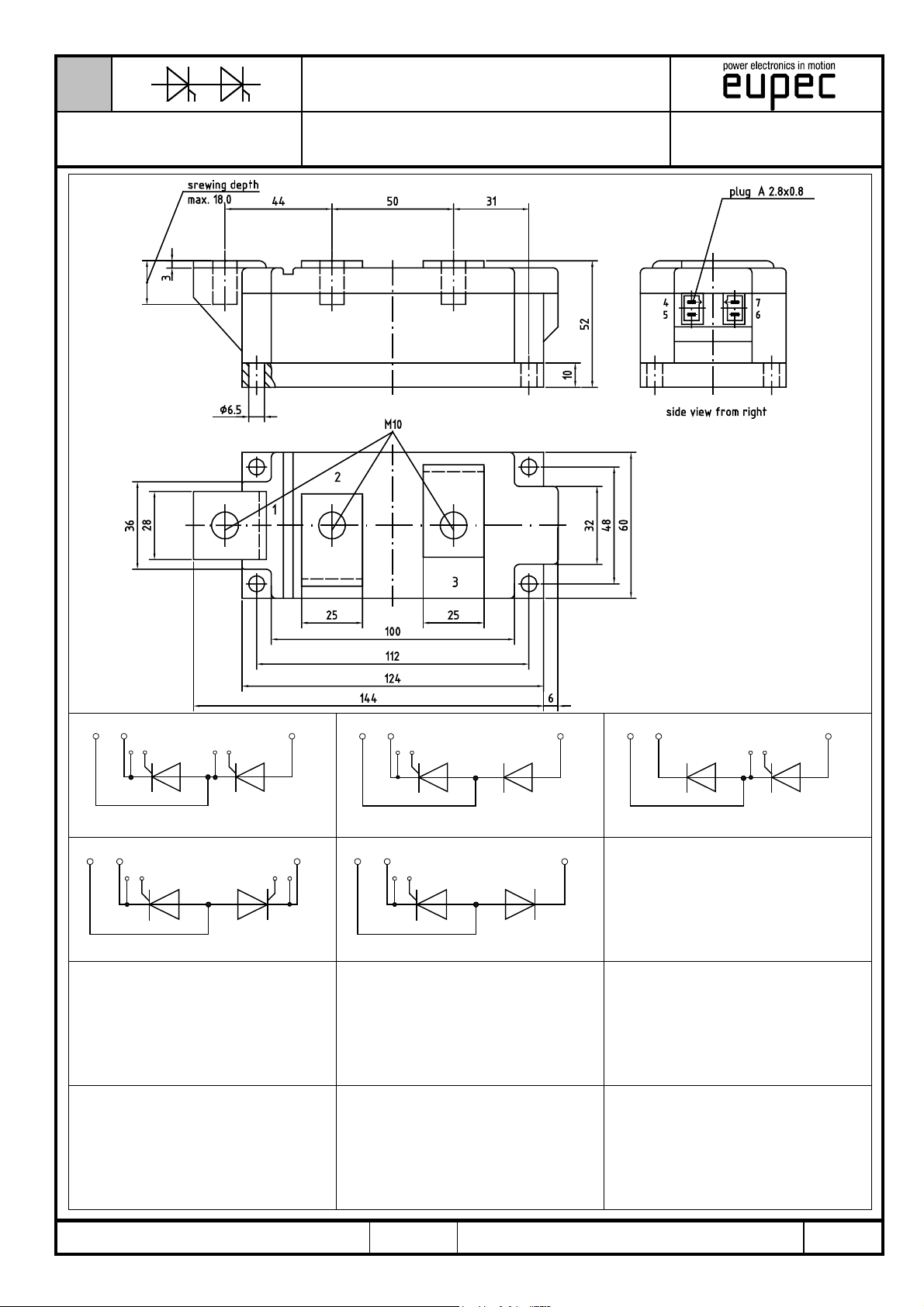
Gehäuse, siehe Seite case, see page 1
Si-Element mit Druckkontakt Si-pellet with pressure contact
Amplifying Gate amplifying gate
Innere Isolation internal insulation AlN
mounting torque Toleranz/tolerance +/- 15% M1 6 Nm
V
V
V
V
V
terminal connection torque Toleranz/tolerance +5%/-10% M2 12 Nm
Gewicht weight G typ. 1500 g
Kriechstrecke creepage distance 19 mm
Schwingfestigkeit vibration resistance f = 50 Hz 50 m/s²

TT 500 N
800
700
P
TAV
[W]
600
500
0 Θ
60°
θ=30°
400
300
200
100
0
0
TT 500 N/1
100 200 300 400 500 600
Bild / Fig. 1
Durchlaßverlustleistung je Zweig / On-state power loss per arm
P
= f(I
TAV
)
TAV
Parameter: Stromflußwi nk el / current conduction angle θ
1200
1000
P
TAV
0
θ
120°
90°
60°
[W]
800
600
θ=30°
400
180°
90°
I
TAV
120°
[A]
180°
DC
140
120
t
C
[°C]
100
80
60
40
20
0
TT 500 N/2
100 200 300 400 500 600
θ=30° 60° 90° 120° 180°
I
TAV
Bild / Fig. 2
Höchstzulässige Gehäusetemperatur / Maximum allowable case temperature
tC = f(I
Strombelastung je Zweig / current load per arm
TAVM
)
Parameter: Stromflußwi nk el / current conduction angle θ
140
120
t
C
[°C]
100
80
60
0 Θ
[A]
0
θ
200
0
0
TT 500 N/3
200 400 600 800 1000
Bild / Fig. 3
Durchlaßverlustleistung je Zweig / On-state power loss per arm
P
= f(I
TAV
Parameter: Stromflußwi nk el / current conduction angle θ
4000
3500
0.015
P
tot
0.020
[W]
0.025
2500
0.030
2000
0.040
0.050
1500
0.060
0.080
1000
0.100
0.120
0.150
0.200
500
0.300
0
TT 500 N/5
)
TAV
R
[°C/W]
thCA
0.010
20 40 60 80 100 1200
0 400 800 1200
tA [°C]
I
TAV
[A]
R-Last
R-load
Id [A]
L-Last
L-load
40
20
0
TT 500 N/4
θ=30° 60° 90° 120° 180° DC
200 400 600 800
I
[A]
TAVM
Bild / Fig. 4
Höchstzulässige Gehäusetemperatur / Maximum allowable case temperature
tC = f(I
Strombelastung je Zweig / current load per arm
TAVM
)
Parameter: Stromflußwi nk el / current conduction angle θ
5000
4000
P
[W]
3000
2000
1000
0.015
tot
0.020
0.025
0.030
0.040
0.050
0.060
0.080
0.100
0.120
0.150
0.200
0
TT 500 N/6
0.010
20 40 60 80 100 1200
R
tA [°C]
thCA
[°C/W]
0
400 800 1200 1600
Id [A]
1000
Bild / Fig. 5
B2 - Zweiplus-Brückens chaltung / Two-pulse bridge circuit
Höchstzulässiger Ausgangsstrom / Maximum rated output current I
Gesamtverlustleist. der Schaltung / total power dissip. of the circuit P
Parameter: Wärmewiderstand zwischen Gehäus e und Umgebung /
thermal resistance case to ambient R
thCA
Bild / Fig. 6
B6 - Sechpuls-Brückenschaltung / Six-pulse bridge circuit
d
tot
Höchstzulässiger Ausgangsstrom / Maximum rated output current I
Gesamtverlustleist. der Schaltung / Total power dissip. of the circuit P
Parameter: Wärmewiderstand zwischen Gehäus e und Umgebung /
thermal resistance case to ambient R
thCA
d
tot

TT 500 N
t
1600
1400
P
1200
[W]
1000
tot
800
600
400
200
0
0.040
0.050
0.060
0.080
0.100
0.120
0.150
0.200
0.300
0.400
0.500
20 40 60 80 100 1200
TT 500 N/7
0.030
0.025
R
thCA
tA [°C]
[°C/W]
0
400 800
200 600 1000 1400
I
RMS
Bild / Fig. 7
W1C - Einphasen-Wechselwegschaltung / Single-phase inverse parallel circuit
Höchstzulässiger Effektivstrom / Maximum ratet RMS current I
Gesamtverlustleist. der Schaltung / Total power dissip. of the
circuit P
tot
Parameter: Wärmewiderstand zwischen Gehäus e und Umgebung/
thermal resistance case to ambient R
thCA
14
12
I
T(OV)M
10
[kA]
8
6
a
b
4
2
[A]
RMS
P
[W]
5000
4000
tot
3000
2000
1000
0.015
0.020
0.025
0.030
0.040
0.050
0.060
0.080
0.100
0.120
0.150
0
20 40 60 80 100 1200 0
TT 500 N/8
R
[°C/W]
thCA
0.010
tA [°C] I
400
800
RMS
Bild / Fig. 8
W3C - Dreiphasen-Wechselwegschaltung / Three-phase inverse parallel circui
Höchstzulässiger Effektivstrom je Phase / Maximum ratet RMS current per
phase I
RMS
Gesamtverlustleist. der Schaltung / Total power dissip. of the circuit P
Parameter: Wärmewiderstand zwischen Gehäus e und Umgebung/
thermal resistance case to ambient R
thCA
10000
5000
4000
3000
2000
Qr [µAs]
1000
700
500
400
300
200
[A]
iTM=
1200
tot
2000A
1000A
100A
50A
20A
0
0.01 0.02
TT 500 N/9
0.06 0.1 0.2 0.4 0.6 0.8 1
0.04
Bild / Fig. 9
Grenzstrom je Zweig I
Maximum overload on- state current per arm I
no-load conditions, VR = 0,8 V
a - tA = 35 °C, verstärkte Luftkühlung / forced cooling
. Belastung aus Leerlauf, VRM = 0,8 V
T(OV)M
RRM
T(OV)M
. Surge current under
b - tA = 45 °C, Luftselbstkühlung / natural cooling
3
2
1
10
vG [V]
5
4
3
2
0
10
5
4
3
2
-1
10
-2
2 3 4 5 2 3 4 52 3 4 5
10
TT 500 N/11
-1
10
o
10
Bild / Fig. 11
Steuercharakteristik mit Zündbereichen / Gate characteristic with triggering
areas, vG = f(iG), vD = 6 V
Parameter: a b c
___________________________________________________
Steuerimpulsdauer / Pulse duration tg [ms] 10 1 0,5
___________________________________________________
Höchstzulässige Spitzensteuerleistung/
Maximum allowable peak gate power [W] 20 40 60
___________________________________________________
t [s]
a
iG [A]
RRM
b
100
1 2 3 4 5 6 7 10 20 30 40 50 70 100
TT 500 N/10
-di/dt [A/µs]
Bild / Fig. 10
Sperrverzögerungsladung / Recovery charge Qr = f(-di/dt)
tvj = t
Parameter: Durchlaßstrom / On-state c urrent i
3
10
t
gd
c
2
10
vjmax
, v
≤ 0,5 V
R
, vRM = 0,8 V
RRM
RRM
TM
[µs]
1
10
0
10
a
b
-1
10
1
10
-1
10
TT 500 N/12
3
2
0
5
10
5 5
2
3
1
10
2
iG [A]
3
2
10
Bild / Fig. 12
Zündverzug / Gate controlled delay time tgd = f(iG)
tvj = 25°C, diG/dt = iGM/1µs
a - maximaler Verlauf / limiting characteristic
b - typischer Verlauf / typical characteristic

TT 500 N
0.08
0.07
Z
(th) JC
0.06
[°C/W]
0
Θ
0.05
0.04
0.03
0.02
0.01
0
-3
10
TT 500 N/13
10
θ=
30°
60°
90°
120°
180°
-2
-1
10
0
10
Bild / Fig. 13
Transienter innerer Wärmewiderstand je Zweig / Transient thermal impedance
per arm Z
Parameter: Stromflußwinkel / current c onduction angle θ
(th)JC
= f(t)
0.1
0.08
Z
(th)JC
[°C/W]
0
θ
0.06
0.04
30°
60°
10
90°
120°
180°
DC
-2
-1
10
0
10
1
10
2
10
t [s]
0.02
0
-3
1
10
2
10
t [s]
10
TT 500 N/14
Bild / Fig. 14
Transienter innerer Wärmewiderstand je Zweig / Transient thermal impedance
per arm Z
Parameter: Stromflußwinkel / current conduction angle θ
Analytische Elemente des transienten Wärmewiderstandes Z
Analytical elements of tr ansient thermal impedance Z
(th)JC
= f(t)
thJC
per arm for DC
thJC
pro Zweig für DC
Pos. n 1 2 3 4 5 6 7
R
τ
thn
[s]
n
[°C/W]
0,00137 0,00486
0,00076 0,0086
0,0114 0,0223 0,0221
0,101 0,56 3,12
Analytische Funktion / Analytical function:
n
Z
thJC
max
= R
Σ
n=1
(1-e )
thn
t
-
τ
n
 Loading...