

Technische Information / Technical Information
Schnelle beschaltungslose Diode
Fast Hard Drive Diode
Features:
D 931 SH 65T
SH
• Speziell entwickelt für beschaltungslosen
• Specially designed for snubberless operation
Betrieb
• Niedrige Verluste, weiches Ausschalten • Low losses, soft recovery
• Volle Sperrfähigkeit bei 140°C mit 50Hz • Full blocking capability at 140°C with 50Hz
• Hohes di/dt und niedriger Wärmewiderstand
durch NTV-Verbindung zwischen Silizium und
Mo-Trägerscheibe
• High di/dt and low thermal resistance by
using low temperature-connection NTV
between silicon wafer and molybdenum
• Elektroaktive Passivierung durch a-C:H • Electroactive passivation by a-C:H
Elektrische Eigenschaften / Electrical properties
Höchstzulässige Werte / Maximum rated values
Periodische Spitzensperrspannung
repetitive peak reverse voltage
Durchlaßstrom-Grenzeffektivwert
RMS forward current
Dauergrenzstrom
mean forward current
Stoßstrom-Grenzwert
surge forward current
Grenzlastintegral
2
t-value
I
Max. Ausschaltverluste
max. turn-off losses
Tvj = 0°C ... T
f = 50Hz
Tc = 60°C. f = 50Hz
TC = 85°C, f = 50Hz
T
= 60°C, f = 50Hz
C
Tvj = T
vj max
Tvj = T
vj max
I
= 2500A, VCL = 2800V,
FM
clamp circuit L
C
= 3µF, DCL = 34DSH65
CL
Tvj = T
vj max
vj max
, Tp = 10ms
, Tp = 10ms
≤ 0,25 µH, R
σ
CL
= 68Ω
V
6500 V
RRM
I
1600 A
FRMSM
I
820
FAVM
1050A A
I
16 kA
FSM
I2t
W
4MW
max
1.28 ⋅ 10
6
A2s
BIP AC / 2002-04-16, Schneider / Keller Release 3 Seite/page
1
Technische Information / Technical Information
Schnelle beschaltungslose Diode
Fast Hard Drive Diode
D 931 SH 65T
SH
Elektrische Eigenschaften / Electrical properties
Charakteristische Werte / Characteristic values
Gleichsperrspannung
continuous direct reverse voltage
Durchlaßspannung
forward voltage
Schleusenspannung
threshold voltage
Ersatzwiderstand
forward slope resistance
Durchlaßrechenkennlinie 250 A ≤ iF ≤ 3200 A
On-state characteristics for calculation
VABiCi Di
=+⋅+⋅ ++⋅ln 1
FFF F
()
Spitzenwert der Durchlaßverzögerungsspannung
peak value of forward recovery voltage
Sperrstrom
reverse current
Rückstromspitze
peak reverse recovery current
Sperrverzögerungsladung
recovered charge
Ausschaltverlust Energie
turn-off energy
Abklingsanftheit
reverse recovery softness factor
)/(
dtdi
0
irr
F
=
RRS
rf
=
)/(
dtdi
max
failure rate λ < 100
estimate value
Tvj = T
, iF = 2500A
vj max
Tvj = T
vj max
Tvj = T
vj max
Tvj = T
vj max
Tvj = T
, diF/dt = 5000A/µs
vj max
I
= 4000A
FM
Tvj = T
I
FM
clamp circuit Lσ ≤ 0,25 µH, R
C
CL
Tvj = T
I
FM
-di
rr
Tvj = T
= V
vj max, vR
= 2500A, VCL = 2800V,
= 3µF, DCL = 34DSH65
vj max
= 2500A, VR = 2800V
/dt
= 1000A/µs, dt = 200ns
(i=0)
vj max
RRM
CL
,
V
R(D)
VF
V
2V
(TO)
rT 1.43
A
B
C
D
V
typ. 430 V
FRM
typ.
max
0.69938
0.00051941
0.0228043
0.067633
3200 V
5.6 V
mΩ
max.
iR 100 mA
IRM max 1300 A
= 68Ω
Qr max 3500 µAs
E
8.0 Ws
off
F
typ. 1,6
RRS
BIP AC / 2002-04-16, Schneider / Keller Release 3 Seite/page
2

Technische Information / Technical Information
Schnelle beschaltungslose Diode
Fast Hard Drive Diode
D 931 SH 65T
SH
Thermische Eigenschaften / Thermal properties
Innerer Wärmewiderstand
thermal resistance, junction to case
Übergangs-Wärmewiderstand
thermal resistance, case to heatsink
Höchstzulässige Sperrschichttemperatur
max. junction temperature
Betriebstemperatur
operating temperature
Lagertemperatur
storage temperature
Kühlfläche / cooling surface
beidseitig / two-sided, DC
Anode / anode, DC
Kathode /cathode, DC
Kühlfläche / cooling surface
beidseitig / two-sided
einseitig / single sided
R
thJC
R
thCK
T
140 °C
vj max
T
0...+140 °C
c op
T
-40...+150 °C
stg
max
max
max
max
max
0,0100
0,0178
0,0230
0.003
0.006
°C/W
°C/W
°C/W
°C/W
°C/W
Mechanische Eigenschaften / Mechanical properties
Gehäuse, siehe Anlage
case, see appendix
Si - Element mit Druckkontakt
Si - pellet with pressure contact
Anpreßkraft
clampig force
Gewicht
weight
Kriechstrecke
creepage distance
Luftstrecke
air distance
Feuchteklasse
humidity classification
Schwingfestigkeit
vibration resistance
DIN 40040
f = 50Hz
Seite 3
65DSH65
F 27...45 kN
G
typ
850 g
30 mm
17 mm
C
50 m/s2
Mit dieser technischen Information werden Halbleiterbauelemente spezifiziert, jedoch keine Eigenschaften zugesichert. Sie gilt in Verbidung mit den zugehörigen technischen Erläuterungen.
This technical Information specifies semiconductor devices but promises no characteristics. It is valid in combination with the belonging technical notes
BIP AC / 2002-04-16, Schneider / Keller Release 3 Seite/page
3
Technische Information / Technical Information
Schnelle beschaltungslose Diode
Fast Hard Drive Diode
D 931 SH 65T
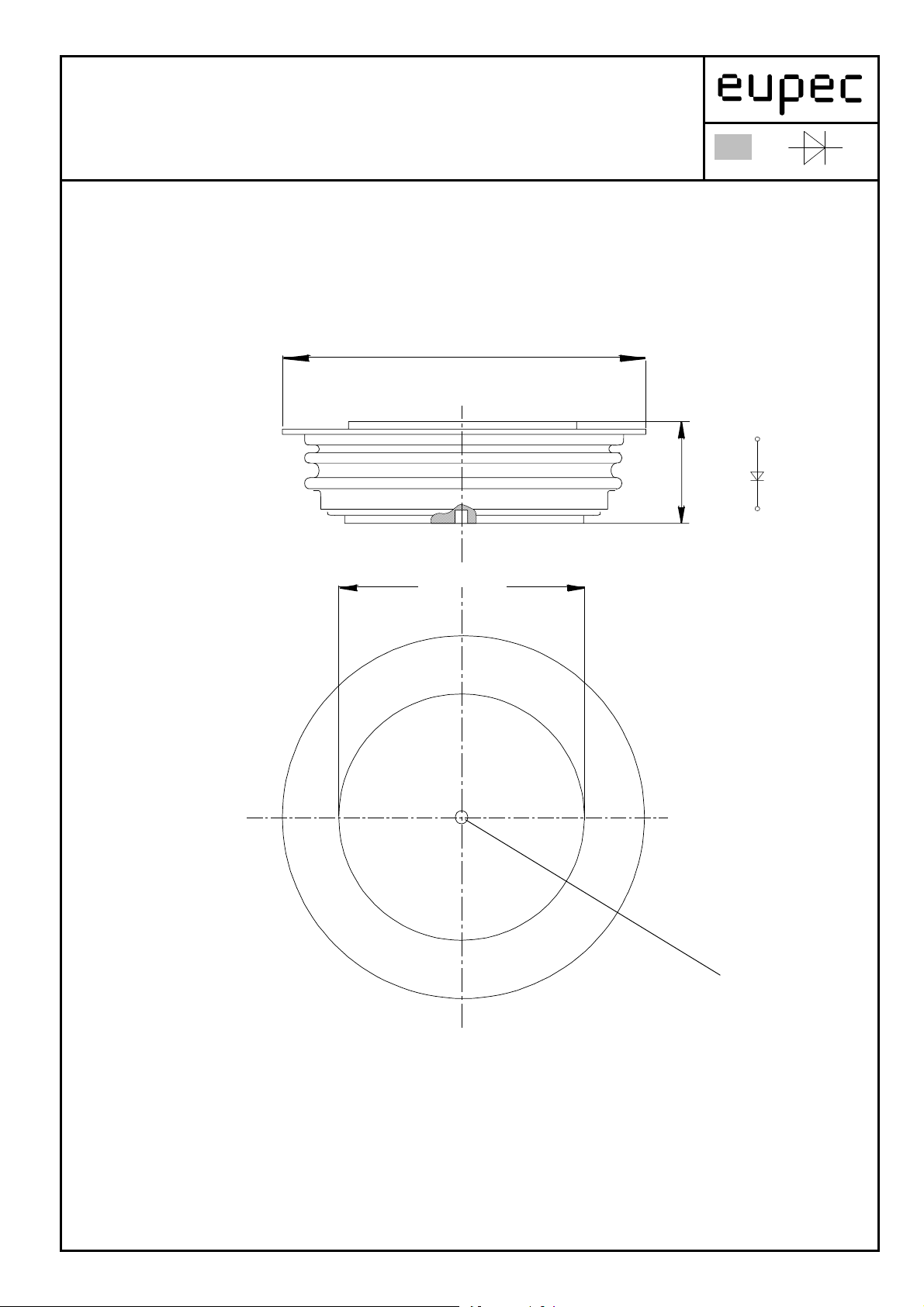
Maßbild / Outline drawing
100 max
SH
A
+-0.5
26
62,8
C
2 center holes
3.5 ×1.8
∅
BIP AC / 2002-04-16, Schneider / Keller Release 3 Seite/page
4

Technische Information / Technical Information
Schnelle beschaltungslose Diode
Fast Hard Drive Diode
Durchlaßkennlinie / On-state characteristics iF = f ( VF )
3500
3000
D 931 SH 65T
upper limit of scatter range
SH
2500
2000
1500
1000
= 25°C
vj
Tvj =140°CT
500
0
012345678
/ [V]
V
F
BIP AC / 2002-04-16, Schneider / Keller Release 3 Seite/page
5

Technische Information / Technical Information
(
)
∑
Schnelle beschaltungslose Diode
Fast Hard Drive Diode
Double side
r [K/W] [s] r [K/W] [s] r [K/W] [s]
1 0,00535 0,504 0,01658 3,77 0,01057 3,77
2 0,00266 0,0879 0,00149 0,381 0,0031 0,287
3 0,00122 0,0156 0,00314 0,0844 0,00251 0,066
4 0,00074 0,00302 0,00114 0,0122 0,0011 0,00957
5 0,00003 0,000819 0,00065 0,00265 0,00052 0,00221
0,01 - 0,023 - 0,0178 -
Σ
Transienter innerer Wärmewiderstand
Transient thermal Impedance Z
cooled
D 931 SH 65T
1)(
nthJCth
n
Cathode side
cooled
= f (t)
(th)JC
−
τ
/
t
n
−⋅=
eRtZ
Anode side
cooled
SH
BIP AC / 2002-04-16, Schneider / Keller Release 3 Seite/page
6

Technische Information / Technical Information
Schnelle beschaltungslose Diode
Fast Hard Drive Diode
Stoßstrom / Grenzlastintegral Charakteristik
Surge current / I²t value characteristics
D 931 SH 65T
I
Sine half-wave, T
= f ( tp ) / i2 dt = f ( tp )
FSM
=140 ° C , v R = 0
vj
SH
1,E+05
/ [A]
FSM
1,E+04
_____ I
1,E+07
i²dt /
1,E+06
−−−−− ∫
1,E+03
0,1 1 10 100
Time / [ms]
1,E+05
BIP AC / 2002-04-16, Schneider / Keller Release 3 Seite/page
7

Technische Information / Technical Information
Schnelle beschaltungslose Diode
Fast Hard Drive Diode
Sperrverzögerungsladung / recovered charge Qr = f ( - di/dt )
Upper limit of scatter range for VF = 5,1V @2500A, 140°C
Conditions: T
clamping circuit CCL = 3 µF RCL = 68Ω 34DSH65
D 931 SH 65T
= 140 ° C
vj
Parameter: I
VCL = 2800 V
FM
SH
4000
3500
3000
2500
2000
IFM =
2500A
1000A
1500
1000
500
0
0 100 200 300 400 500 600 700 800 900 1000
BIP AC / 2002-04-16, Schneider / Keller Release 3 Seite/page
500A
100A
-di/dt / [A/µs]
8

Technische Information / Technical Information
Schnelle beschaltungslose Diode
Fast Hard Drive Diode
Rückstromspitze / peak reverse recovery current I
Upper limit of scatter range for VF = 5,1V @2500A, 140°C
Conditions: T
clamping circuit CCL = 3 µF RCL = 68Ω 34DSH65
D 931 SH 65T
= 140 ° C
vj
Parameter: I
VCL = 2800 V
FM
RM
SH
= f ( - di/dt )
1500
1250
1000
750
IFM =
2500A
1000A
500
250
0
0 100 200 300 400 500 600 700 800 900 1000
BIP AC / 2002-04-16, Schneider / Keller Release 3 Seite/page
500A
100A
-di/dt / [A/µs]
9

Technische Information / Technical Information
Schnelle beschaltungslose Diode
Fast Hard Drive Diode
Ausschaltverlust Energie / turn-off energy E
Upper limit of scatter range for VF = 5,1V @2500A, 140°C
Conditions: T
clamping circuit CCL = 3 µF RCL = 68Ω 34DSH65
10
9
D 931 SH 65T
= f ( - di/dt )
off
= 140 ° C
vj
Parameter: I
VCL = 2800 V
FM
SH
8
7
6
5
4
3
2
IFM =
2500A
1000A
500A
1
100A
0
0 100 200 300 400 500 600 700 800 900 1000
-di/dt / [A/µs]
BIP AC / 2002-04-16, Schneider / Keller Release 3 Seite/page
10

Technische Information / Technical Information
/
Schnelle beschaltungslose Diode
Fast Hard Drive Diode
500
400
300
Spitzen-Durchlassverzögerungsspannung
peak forward recovery voltage V
typische Abhängigkeit / typical dependence
D 931 SH 65T
Tvj = 140°C, IFM = 4000A
= f ( diF/dt )
FRM
SH
[V]
FRM
V
200
100
0
0 1000 2000 3000 4000 5000 6000
di
dt [A/µs]
F
BIP AC / 2002-04-16, Schneider / Keller Release 3 Seite/page
11
 Loading...