

Page 1

Never stop thinking.
Power Management & Supply
ICE3BRxx65J(Z)(G)
CoolSET®-F3R (DIP-8, DIP-7 & DSO-16/12)
new Jitter version Design Guide
Application Note, V 2.2, June 2010
Page 2

Edition 2010-06-20
Published by Infineon Technologies Asia Pacific,
8 Kallang Sector,
349282 Singapore, Singapore
© Infineon Technologies AP 2008.
All Rights Reserved.
Attention please!
The information herein is given to describe certain components and shall not be considered as a guarantee
of characteristics.
Terms of delivery and rights to technical change reserved.
We hereby disclaim any and all warranties, including but not limited to warranties of non-infringement,
regarding circuits, descriptions and charts stated herein.
Information
For further information on technology, delivery terms and conditions and prices please contact your nearest
Infineon Technologies Office (www.infineon.com).
Warnings
Due to technical requirements components may contain dangerous substances. For information on the types
in question please contact your nearest Infineon Technologies Office.
Infineon Technologies Components may only be used in life-support devices or systems with the express
written approval of Infineon Technologies, if a failure of such components can reasonably be expected to
cause the failure of that life-support device or system, or to affect the safety or effectiveness of that device or
system. Life support devices or systems are intended to be implanted in the human body, or to support
and/or maintain and sustain and/or protect human life. If they fail, it is reasonable to assume that the health
of the user or other persons may be endangered.
Page 3

ICE3BRXX65J(Z)(G)
Revision History: 2010-06-20 V2.2
Previous Version: V2.1a
Page Subjects (major changes since last revision)
Add ICE3BR4765JZ
CoolSET®-F3R (DIP-8, DIP-7 & DSO-16/12) new Jitter version Design Guide:
License to Infineon Technologies Asia Pacific Pte Ltd AN-PS0025
Kyaw Zin Min
Kok Siu Kam Eric
We Listen to Your Comments
Any information within this document that you feel is wrong, unclear or missing at all?
Your feedback will help us to continuously improve the quality of this document.
Please send your proposal (including a reference to this document) to:
ap-lab.admin@infineon.com
Page 4

ICE3BRXX65J(Z)(G)
Table of Contents Page
Application Note 4 2010-06-20
1 Introduction ...................................................................................................................................5
2 List of Features .............................................................................................................................5
3 Package..........................................................................................................................................5
4 Block Diagram ...............................................................................................................................7
5 Typical Application Circuit...........................................................................................................8
6 Functional description and component design .........................................................................9
6.1 Startup time .....................................................................................................................................9
6.1.1 Vcc capacitor...................................................................................................................................9
6.2 Soft Start .......................................................................................................................................10
6.3 Low standby power - Active Burst Mode.......................................................................................10
6.3.1 Entering Active Burst Mode...........................................................................................................10
6.3.2 Working in Active Burst Mode .......................................................................................................11
6.3.3 Leaving Active Burst Mode ...........................................................................................................12
6.3.4 Minimum VCC supply voltage during burst mode...........................................................................13
6.4 Low EMI noise...............................................................................................................................13
6.4.1 Frequency jittering.........................................................................................................................13
6.4.2 Soft gate drive ...............................................................................................................................13
6.4.3 Other suggestions to solve EMI issue...........................................................................................14
6.5 Tight maximum power control - Propagation delay compensation ...............................................14
6.6 Protection Features .......................................................................................................................15
6.6.1 Auto Restart Protection Mode .......................................................................................................15
6.6.2 Blanking Time for over load protection .........................................................................................16
6.6.3 User defined protection by external protection enable pin............................................................17
7 Input power curve .......................................................................................................................17
8 Layout Recommendation ...........................................................................................................20
9 Product portfolio of CoolSET®-F3R (DIP-8, DIP-7 & DSO-16/12) new Jitter version ............20
10 Useful formula & external component design .........................................................................21
11 References ...................................................................................................................................22
Page 5

ICE3BRXX65J(Z)(G)
Application Note 5 2010-06-20
1 Introduction
The CoolSET®-F3R, ICE3BRxx65J(Z)(G) is the latest development of the CoolSET®-F3. It is a PWM
controller with power MOSFET and startup cell in a DIP or DSO package. The switching frequency is running
at 65 KHz and it targets for DVD player, set-top box, portable game console, auxiliary power supply, etc.
The ICE3BRxx65J(Z)(G) adopts the BiCMOS technology and provides a wider Vcc operating range up to
25V. It inherits the proven good features of CoolSET
®
-F3 such as the active burst mode achieving the lowest
standby power, the propagation delay compensation making the most precise current limit control in wide
input voltage range, etc. In addition, it also adds on some useful features such as built-in soft start time, builtin basic with extendable blanking time for over load protection and built-in switching frequency modulation (
frequency jittering ), external auto-restart enable, etc.
2 List of Features
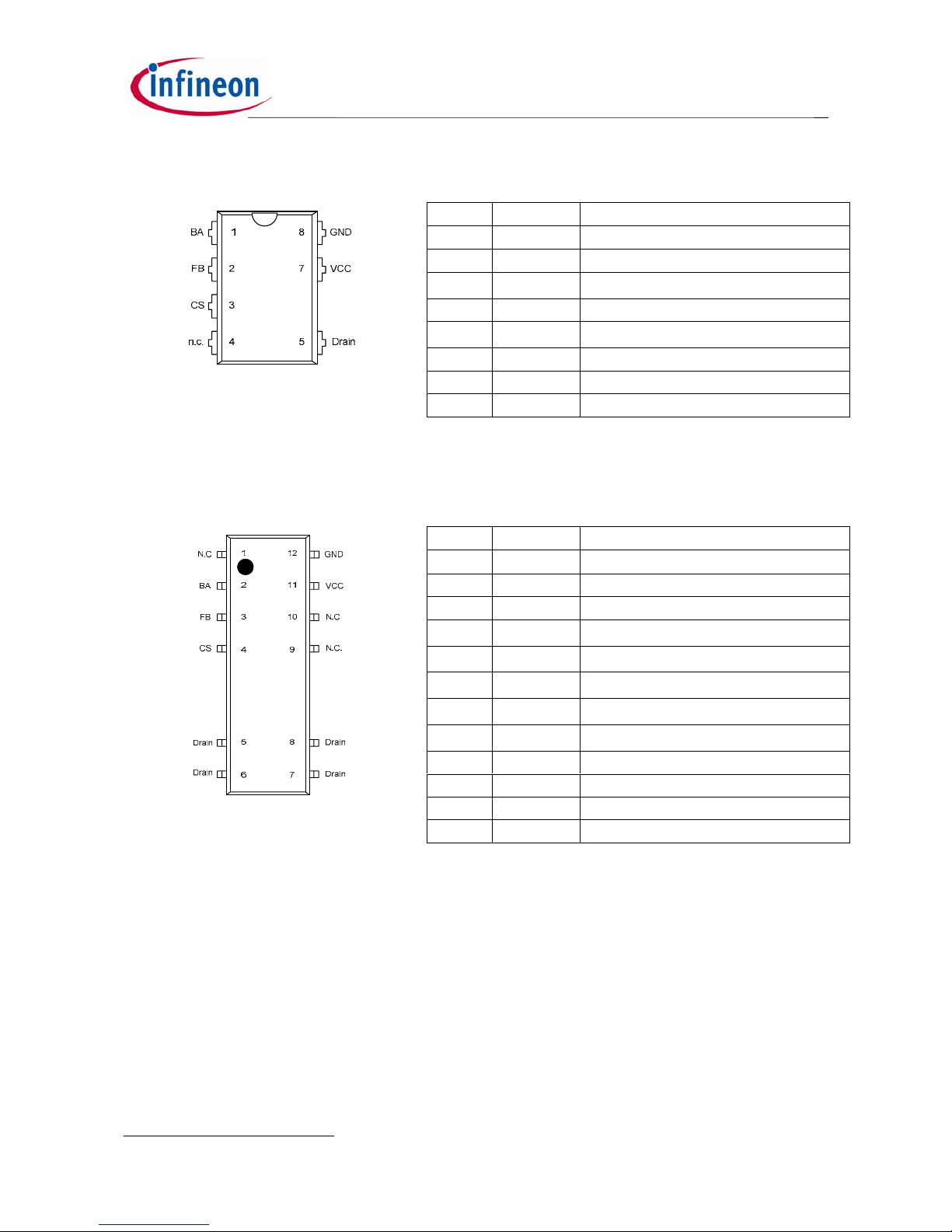
3 Package
The package for F3R ICE3BRXX65J Jitter mode product is DIP-8.
Figure 1 Pin configuration –
ICE3BRxx65J
1
at Tj=110°C
650V avalanche rugged CoolSET® with built-in Startup Cell
Active Burst Mode for lowest Standby Power
Fast load jump response in Active Burst Mode
65 kHz internally fixed switching frequency
Auto Restart Protection Mode for Over-load, Open Loop, Vcc Undervoltage, Over temperature & Vcc
Over-voltage
Built-in Soft Start
Built-in blanking window with extendable blanking time for short duration high current
External auto-restart enable pin
Max Duty Cycle 75%
Overall tolerance of Current Limiting < ±5%
Internal PWM Leading Edge Blanking
BiCMOS technology provides wide VCC range
Built-in Frequency jitter feature and soft driving for low EMI
Pin Name Description
1 BA extended Blanking & Auto-restart enable
2 FB FeedBack
3 CS
Current Sense / 650V
1
CoolMOS® Source
4 Drain
650V
1
CoolMOS® Drain
5 Drain
650V
1
CoolMOS® Drain
6 n.c. Not Connected
7 VCC Controller Supply Voltage
8 GND Controller Ground
1
6
7
8
4
3
2
5
GND BA
FB
CS
VCC
n.c
Drain
Drain
Page 6
ICE3BRXX65J(Z)(G)
Application Note 6 2010-06-20
The package for F3R ICE3BRXX65JZ Jitter mode product is DIP-7.
Figure 2 Pin configuration – ICE3BRxx65JZ
The package for F3R ICE3BRXX65JG Jitter mode product is DSO-16/12.
Figure 3 Pin configuration – ICE3BRxx65JG
1
at Tj=110°C
Pin Name Description
1 BA extended Blanking & Auto-restart enable
2 FB FeedBack
3 CS
Current Sense / 650V
1
CoolMOS® Source
4 n.c. Not connected
5 Drain
650V
1
CoolMOS® Drain
6 - No Pin
7 VCC Controller Supply Voltage
8 GND Controller Ground
Pin Name Description
1 N.C. Not Connected
2 BA extended Blanking & Auto-restart enable
3 FB FeedBack
4 CS
Current Sense / 650V
1
CoolMOS® Source
5 Drain
650V
1
CoolMOS® Drain
6 Drain
650V
1
CoolMOS® Drain
7 Drain
650V
1
CoolMOS® Drain
8 Drain
650V
1
CoolMOS® Drain
9 N.C. Not Connected
10 N.C. Not Connected
11 VCC Controller Supply Voltage
12 GND Controller Ground
Page 7

ICE3BRXX65J(Z)(G)
Application Note 7 2010-06-20
4 Block Diagram
Figure 4 Block Diagram of ICE3BRXX65J(Z)(G)
Page 8

ICE3BRXX65J(Z)(G)
Application Note 8 2010-06-20
5 Typical Application Circuit
Figure 5 Typical application circuit with ICE3BR4765J 12W 5V
5V/2 . 4A
COM
F1
3. 15 A
C1
0. 1uF/2 75V
EMI
2 x 4 7mH, 0. 4A
BR1
2KBB80R
+
C2
47uF/ 400V
R1
150k /2W
D1
UF4005
C3
2. 2nF/4 00V
2
1
3
4
IC2
SFH 617A- 3
C7
10nF
+
C5 22uF/50V
C6
0. 1uF
D2
1N41 48
R2
510R
Rc6
470R
R4
1. 5R
IC3
TL431
Cc2
1nF
Rc4
6. 8k
Cc1
1uF
Rc2
0R
Rc3
10k
+
C21
1800 uF/ 25V
L2 1
1. 5uH
+
C22
220u F/25V
85V - 26 5V ac
12W 5V SMPS Demoboard with ICE3BR4765J(V0.2)
Eric Kok, Kyaw Zin Min / 8 Nov 2007
L1
L
N
Rc5
2. 2K
Rc1
10 k
C4
1nF/ 250V, Y1
C8
1nF
R4A
15R
Rc3A
*
C23
*
R21 *
ZD1
24V
R3
39R
*SG 1
*SG 2
65
4
3
9
2
1
TR1 830uH
BA
CS
Vcc
DRAIN
GND FB
ICE3BR4765 J
345
1
82 7
IC1
C13
0. 1uF/50V
L2
D21
SB540
Page 9

ICE3BRXX65J(Z)(G)
Application Note 9 2010-06-20
6 Functional description and component design
6.1 Startup time
Startup time is counted from applying input voltage to IC turn on. ICE3BRXX65J(Z)(G) has a startup cell
which is connected to input bulk capacitor. When there is input voltage, the startup cell will act as a constant
current source to charge up the Vcc capacitor and supply energy to the IC. When the Vcc capacitor reaches
the Vcc_on threshold 18V, the IC turns on. Then the startup cell is turned off and the Vcc is supplied by the
auxiliary winding. Start up time is independent from the AC line input voltage and it can be calculated by the
equation (1). Figure 6 shows the start up time of 85Vac line input.
3arg eVCCch
VccVCCon
STARTUP
I
CV
t
⋅
=
(1)
where, I
VCCcharge3
: constant current to charge Vcc capacitor ( 0.7mA ),
V
VCCon
: IC turns on threshold ( 18V ), C
VCC
: Vcc capacitor
Pls refer to the datasheet for the symbol used in the equation.
Channel 1; C1 : CS Voltage (V
CS
)
Channel 2; C2 : Supply Voltage (V
CC
)
Channel 3; C3 : FB voltage (V
FB
)
Channel 4; C4 : BA Voltage (V
BA
)
Startup time = 0.54s
Startup delay time @ Vin=85Vac & 12W
load
Figure 6 The startup delay time at AC line input voltage of 85Vac
Precaution : For a typical application, start up should be VCC ramps up first, other pin (such as FB pin)
voltage will follow VCC voltage to ramp up. It is recommended not to have any voltage on other
pins (such as FB; BA and CS) before VCC ramps up.
6.1.1 Vcc capacitor
The minimum value of the Vcc capacitor is determined by voltage drop during the soft start time. The formula
is expressed in equation (2).
3
2
2sup
⋅
⋅
=
CChys
ssVCC
VCC
V
tI
C
(2)
where, I
VCCsup2
: IC consumption current ( 4.2mA ), tss : soft start time ( 20ms ),
V
CChys
: Vcc turn-on/off hysteresis voltage ( 7.5V )
Therefore, the minimum Vcc capacitance can be 7.4µF. In order to give more margins, 22uF is taken for the
design. The startup time t
STARTUP
is then 0.528s. The measured start up time is 0.54s (Figure 6). A 0.1uF
filtering capacitor is always needed to add as near as possible to the Vcc pin to filter the high frequency
noise. The filter capacitor C6 and the auxiliary series resistor R2 form a R-C filter which can effectively filter
the transformer switching noise from auxiliary winding going into the IC.
0.54s
V
CS
V
CC
V
FB
VBA
Page 10

ICE3BRXX65J(Z)(G)
Application Note 10 2010-06-20
6.2 Soft Start
When the IC is turned on after the Startup time, a digital soft start circuit is activated. A gradually increased
soft start voltage is generated by the digital soft start circuit, which in turn releases the duty cycle gradually
from zero. The duty cycle increases to maximum (which is limited by the transformer design) at the end of
the soft start period. When the soft start time ends, IC goes into normal mode and the duty cycle is controlled
by the FB signal. The soft start time is set at 20ms for maximum load. The soft start time is load dependent;
shorter soft start time with lighter load.
Figure 7 shows the soft start behavior at 85Vac input. The primary peak current increases slowly to the
maximum in the soft start period.
Channel 1; C1 : CS Voltage (V
CS
)
Channel 2; C2 : Supply Voltage (V
CC
)
Channel 3; C3 : FB voltage (V
FB
)
Channel 4; C4 : BA Voltage (V
BA
)
Soft start time = 20ms
20ms built in SoftStart time @
Vin=85Vac & 12W load
Figure 7 Soft start at AC line input voltage of 85Vac
6.3 Low standby power - Active Burst Mode
The IC will enter Active Burst Mode function at light load condition which enables the system to achieve the
lowest standby power requirement of less than 50mW. Active Burst Mode means the IC is always in the
active state and can therefore immediately respond to any changes on the FB signal, V
FB
.
6.3.1 Entering Active Burst Mode
Because of the current mode control scheme, the feedback voltage VFB actually controls the power delivery
to output. An important relationship between the V
CS
and the VFB is expressed in equation (3).
RampOffsetVCSFB
VAVV
−
+⋅= (3)
where, V
FB
:feedback voltage, VCS:current sense voltage, AV:PWM OP gain, V
Offset-Ramp
:voltage ramp offset
When the output load reduces, the feedback voltage V
FB
drops. If the VFB stays below 1.35V for 20ms, the IC
enters into the Active Burst Mode. The threshold power to enter burst mode is expressed in equation (4).
SW
Vsense
RampOffsetFBC
PSW
sense
CS
PSW
p
PenterBURST
f
AR
VV
Lf
R
V
LfILP ⋅
⋅
−
⋅⋅=⋅⋅⋅=⋅⋅⋅=
−
2
5
22
_
)(
2
1
)(
2
1
2
1
(4)
where, L
p
: transformer primary inductance
R
sense
: current sense resistance, fsw: switching frequency, V
FBC5
: Feedback level to enter burst mode
Figure 8 shows the waveform with the load change from nominal load to light load. After the 20ms blanking
time IC goes into burst mode.
20ms
1V
VCS
V
BA
V
CC
V
FB
Page 11

ICE3BRXX65J(Z)(G)
Application Note 11 2010-06-20
Channel 1; C1 : Drain-Source Voltage (VDS)
Channel 2; C2 : Supply Voltage (V
CC
)
Channel 3; C3 : FB voltage (V
FB
)
Channel 4; C4 : BA Voltage (V
BA
)
Entering Active Burst mode with preset
time 20ms when load changes from full to
light @ Vin=85Vac
Figure 8 Entering Burst Mode
6.3.2 Working in Active Burst Mode
In the active burst mode, the IC is constantly monitoring the output voltage by feedback pin, VFB, which
controls burst duty cycle and burst frequency. The burst “ON” starts when V
FB
reaches 3.5V and it stops
when V
FB
is dropped to 3.0V. During burst “ON”, the primary current limit is set to 34% of maximum peak
current (V
CS
=0.34V) to reduce the conduction losses and to avoid audible noise. The FB voltage is changing
like a saw tooth between 3.0V and 3.5V. The corresponding secondary output ripple (peak to peak) is
controlled to be small. It can be calculated by equation (5).
FB
TLoptoFB
opto
pprippleout
V
GGR
R
V ∆⋅
⋅⋅
=
431
__
(5)
where, R
opto
: series resistor with opto-coupler at secondary side (e.g. Rc6 in Figure 5), RFB : IC internal pull
up resistor connected to FB pin (R
FB
=15.4K), G
opto
: current transfer gain of opto-coupler, G
TL431
: voltage
transfer gain of the loop compensation network (e.g. Rc1, Rc2, Rc3, Rc4, Cc1, Cc2 in Figure 5),
∆
V
FB
:
feedback voltage change (0.5V)
Usually there is a noise coupling capacitor at the FB pin to filter the switching noise and spike (e.g. C8 in
Figure 5). However, if this capacitor is too large (>10nF), it would affect the normal operation of the
controller. This capacitor should be as small as possible (without the capacitor is the best). In the mean time,
it is found that this filter capacitor will also affect the output ripple voltage during burst mode; larger
capacitance will get larger ripple voltage and smaller capacitance get lower ripple voltage.
Figure 9 is the output ripple waveform of the 12W demo board. The burst ripple voltage is about 50mV.
Channel 2; C2 : Output ripple Voltage (V
o
)
Output ripple voltage at light load @ Vin=85Vac
Figure 9 Output ripple during Active Burst Mode at light load
VDS
V
BA
20ms
50mV
VFB
V
CC
V
o
Page 12

ICE3BRXX65J(Z)(G)
Application Note 12 2010-06-20
6.3.3 Leaving Active Burst Mode
When the output load increases to be higher than the maximum burst power, P
burst_max
, V
out
will drop and VFB
will rise up fast to exceed 4.0V. The system leaves burst mode immediately when V
FB
reaches 4.0V. Once
system leaves burst mode, the current sense voltage limit, V
CS_MAX
, is released to 1V, the feedback voltage
V
FB
swings back to the normal control level.
The leaving burst power threshold (i.e. maximum power to be handled during burst operation) is expressed
in equation (6).
max_
2
max_
2
max_max_
1156.0)34.0(5.0)34.0(5.0
inSW
sense
CS
PSWpPburst
Pf
R
V
LfILP ⋅=⋅⋅⋅⋅=⋅⋅⋅⋅= (6)
where,
max_p
I : maximum primary peak current, V
CS_max
: current limit threshold at CS pin, P
in_max
: maximum
input power
The calculated maximum power in burst mode is around 6.76% of P
in_max
. However, the actual power can be
higher as it would include propagation delay time.
The leave burst mode timing diagram is shown in Figure 10. The maximum output drop during the transition
can be estimated in equation (7).
431431
max__
75.0
)
2
5.33
4(
TLoptoFB
opto
TLoptoFB
opto
dropout
GGR
R
GGR
R
V
⋅⋅
⋅
=
+
−⋅
⋅⋅
= (7)
Figure 10 Timing diagram of leaving burst mode
Figure 11 is the captured waveform when there is a load jump from light load to full load. The output ripple
drop during the transition is about 88mV.
Channel 1; C1 : CS Voltage (V
CS
)
Channel 2; C2 : Output Voltage (V
o
)
Channel 3; C3 : FB voltage (V
FB
)
Leaving Active Burst mode when load change from
light to full @ Vin=85Vac
Figure 11 Leaving burst mode waveform
V
FB
V
out_AV
V
out_drop_max
3.5V
3.0V
V
out
4.0V
V
CS
0.34V
1.03V
88mV
Vo
VFB
V
CS
Page 13

ICE3BRXX65J(Z)(G)
Application Note 13 2010-06-20
6.3.4 Minimum VCC supply voltage during burst mode
It is particularly important that the Vcc voltage must stay above V
VCCoff
(i.e. 10.5V). Otherwise, the expected
low standby power cannot be achieved. The IC will go into auto-restart mode instead of Active Burst Mode. A
reference Vcc circuit is presented in Figure 5. This is for a low cost transformer design where the transformer
coupling is not too good. Thus the circuit R3 and Zd1 is added to clamp the Vcc voltage exceeding 25V in
extreme case such as high load and the Vcc OVP protection is triggered. If the transformer coupling is good,
this circuit is not needed.
6.4 Low EMI noise
6.4.1 Frequency jittering
The IC is running at a fixed frequency of 65 KHz with jittering frequency at +/-2.6 KHz in a switching
modulation period of 4ms. This kind of frequency modulation can effectively help to obtain a low EMI noise
level particularly for conducted EMI. The jittering frequency measured is 63.8 KHz ~ 67.4 KHz (refer to
Figure 12).
Channel 1; C1 : Drain to Source Voltage (V
DS
)
Frequency jittering at full load @ Vin=85Vac
Figure 12 Switching frequency jittering ( Vds )
6.4.2 Soft gate drive
The gate soft driving is to split the gate driving slope into 2 so that the MOSFET turns on speed is relatively
slower comparing to a single slope drive (see Figure 13). In this way, the high I/t noise is greatly reduced
and the noise signal reflected in the EMI spectrum is also reduced.
Figure 13 Soft gate drive waveform
67.4kHz
63.8kHz
VDS
Page 14

ICE3BRXX65J(Z)(G)
Application Note 14 2010-06-20
6.4.3 Other suggestions to solve EMI issue
Some more suggestions to improve the EMI performance and is listed below.
1. Add capacitor (C
ds
) at the drain source pin: it can slow down the turn off speed of the MOSFET and
the high V/t noise will be reduced and so is the EMI noise. The drawback is more energy will be
dissipated due to slower turn off speed of MOSFET.
2. Add snubber circuit to the output rectifier: Most of the radiated EMI noise comes out from the output
of the system esp. for a system with output cable. Adding snubber circuit (R21 and C23) to the
output rectifier is a more direct way to suppress those EMI noise (refer to Figure 5).
6.5 Tight maximum power control - Propagation delay compensation
The maximum power of the system is changed with the input voltage; higher voltage got higher maximum
power. This is due to the propagation delay of the IC and the different rise time of the primary current under
different input voltage. The propagation delay time is around 200ns. But if the primary current rise time is
faster, the maximum power will increase. The power difference can be as high as >14% between high line
and low line. In order to make the maximum power control become tight, a propagation delay compensation
network is implemented so that the power difference is greatly reduced to best around 2%. Figure 14 shows
the compensation scheme of the IC. The equation (8) explains the rate of change of the current sense
voltage is directly proportional to the input voltage and current sense resistor. For a DCM operation, the
operating range for the dV
sense
/dt is from 0.1 to 0.7. It can show in Figure 14 that higher dV
sense
/dt will give
more compensation; i.e. lower value of V
sense
.
p
in
sense
sense
p
in
sense
p
sense
p
in
p
L
V
R
dt
dV
L
V
R
dt
dI
R
L
V
dt
dI
⋅=⇒⋅=⋅⇒=
(8)
where, I
p
: primary peak current, V
in
: input voltage, Lp : primary inductance of the transformer,
V
sense
: current sense voltage, R
sense
: current sense resistor
The measured maximum input power for the 12W demo boards at 85Vac and 265Vac shows ±1.71% of
maximum input power. This function is limited to discontinuous conduction mode flyback converter only.
0,9
0,95
1
1,05
1,1
1,15
1,2
1,25
1,3
0 0,2 0,4 0,6 0,8 1 1,2 1,4 1,6 1,8 2
with compensation
without compensation
dt
dV
Sense
s
V
µ
Sense
V
V
Figure 14 Propagation delay compensation curve
Page 15

ICE3BRXX65J(Z)(G)
Application Note 15 2010-06-20
6.6 Protection Features
The IC provides several protection features which lead to the Auto Restart Protection Mode. The following
table shows the conditions of the system failure and the associate protection mode.
Protection function Failure condition Protection Mode
Vcc Over-voltage
1. Vcc > 25.5V or
2. Vcc > 20.5V & FB > 4.0V & during soft start period
Auto Restart
Over-temperature
(controller junction)
T
J
> 130°C Auto Restart
Over-load / Open loop
V
FB
> 4.0V and VBA > 4.0V
(Blanking time counted from charging V
BA
from 0.9V to
4.0V )
Auto Restart
Vcc Under-voltage / short
Opto-coupler
Vcc < 10.5V Auto Restart
Auto-restart enable VBA < 0.33V Auto Restart
Table 1 Protection functions and failure conditions
The 25.5V OVP protection is inactivated during burst mode so that it can achieve lower standby power
performance.
6.6.1 Auto Restart Protection Mode
When the failure condition meets the auto restart protection mode, the IC will go into auto-restart. The
switching pulse will stop. Then the Vcc voltage will drop. When the Vcc voltage drops to 10.5V, the startup
cell will turn on again. The Vcc voltage is then charged up. When it hits 18V, the IC will turn on and the
startup cell will turn off. It would then start the startup phase with soft start. After the startup phase the failure
condition is checked to determine whether the fault persists. If the fault is removed, it will go to normal
operation. Otherwise, the IC will repeat the auto restart protection and the switching pulse stop again.
Figure 15 shows the switching waveform of the V
CC
and the feedback voltage VFB when the output is
overloaded by shorting the outputs. The IC is turned on at V
CC
= 18V. After going through the startup phase,
IC is off again due to the presence of the fault. V
CC
is discharged until 10.5V. Then, the Startup Cell is
activated again to charge up capacitor at V
CC
that initiates another restart cycle.
Channel 1; C1 : Drain-Source Voltage (V
DS
)
Channel 2; C2 : Supply Voltage (V
CC
)
Channel 3; C3 : Feedback Voltage ( V
FB )
Channel 4; C4 : BA voltage ( V
BA )
System enters auto restart mode when output
voltage short circuit @ Vin=85Vac
Figure 15 Auto Restart Mode
VDS
Vcc
VFB
VBA
Page 16

ICE3BRXX65J(Z)(G)
Application Note 16 2010-06-20
6.6.2 Blanking Time for over load protection
The IC controller provides a blanking window before entering into the auto restart mode due to output
overload/short circuit. The purpose is to ensure that the system will not enter protection mode unintentionally.
There are 2 kinds of the blanking time; basic and the extendable. The basic one is a built-in feature which is
set at 20ms. The extendable one is to extend the basic one with a user defined additional blanking time. The
extendable blanking time can be achieved by adding a capacitor, C
BK
to the BA pin. When there is over load
occurred ( V
FB
> 4V ), the CBK capacitor will be charged up by a constant current source, IBK ( 13uA ) from
0.9V to 4.0V. Then the auto restart protection will be activated. The charging time from 0.9V to 4.0V to the
C
BK
capacitor is the extended blanking time. The total blanking time is the addition of the basic and the
extended blanking time.
BK
BK
BK
blanking
Cms
I
C
msExtendedBasict *5.23846120
*)9.00.4(
20 +=
−
+=+= (9)
The measured total blanking time showing in Figure 17 is 45ms using C
BK
=0.1uF.
In case of output overload or short circuit, the transferred power during the blanking period is limited to the
maximum power defined by the value of the sense resistor R
sense
.
The noise level in BA pin can be quite high particularly in some high power application. In order to avoid mistriggering of other protection features, it is recommended to add a minimum 100pF filter capacitor at BA pin.
The maximum capacitor added at BA is restricted to be less than 0.65uF. Otherwise, the IC cannot be
startup properly.
Channel 1; C1 : Output Voltage ( V
o
)
Channel 2; C2 : Output current ( I
o
)
Channel 3; C3 : Feedback Voltage ( V
FB )
Channel 4; C4 : BA voltage ( V
BA )
Blanking time to enter auto-restart mode : 19ms
Over load protection without extended blanking
time;Cba=100pF @ Vin=85Vac and output power
step from 2.4A to 4A load
Figure 16 Blanking window for output over load protection ( basic blanking time )
Channel 1; C1 : Output Voltage ( V
o
)
Channel 2; C2 : Output current ( I
o
)
Channel 3; C3 : Feedback Voltage ( V
FB )
Channel 4; C4 : BA voltage ( V
BA )
Blanking time to enter auto-restart mode : 71ms
Over load protection with extended blanking
time;C7 = 0.22µF @ Vin=85Vac and output power
step from 2.4A to 4A load
Figure 17 Blanking window for output overload protection ( extended blanking time=24ms with
C
BK
=0.1uF )
19ms
52ms
19ms
Vo
Io
V
FB
V
BA
Vo
Io
V
FB
V
BA
Page 17

ICE3BRXX65J(Z)(G)
Application Note 17 2010-06-20
6.6.3 User defined protection by external protection enable pin
Although there are lots of pre-defined Auto Restart Protection is implemented in the IC, customer still can
have some tailor-made protection for the application needs by pulling down the BA pin to lower 0.33V. When
BA pin lower than 0.33V, the gate drive switching will be stopped and IC will enter to auto restart mode until
the external auto restart enable signal released.
Figure 18 User defined Auto Restart Protection circuit
7 Input power curve
The purpose of the input power curve is to simplify the selection of the CoolSET® device. The curve is a
function of ambient temperature to the input power of the system in which the input filter loss, bridge rectifier
loss and the MOSFET power loss are considered. The only information needed is the required output power,
the input voltage range, the operating ambient temperature and the efficiency of the system. The required
input power can then be calculated as equation (10).
η
o
in
P
P =
(10)
where P
in
: input power, Po : output power, : efficiency
It then simply looks up the closed input power at the required ambient temperature from the input power
curve.
The input power curves for the CoolSET-F3R (DIP-8 & DIP-7) family are listed below.
ICE3BR0665J : Vin=85Vac~265Vac ICE3BR0665J : Vin=230Vac±15%
Figure 19 Input power curve for ICE3BR0665J
Ambient Temperature [°C]
Input power (230Vac) [W]
PI-002-ICE3X2565_230Vac
0
10
20
30
40
50
60
70
80
90
100
0 102030405060708090100110120130
Ambient Temperature [°C]
Input power (85~265Vac) [W]
PI-001-ICE3X2565_85Vac
0
6
12
18
24
30
36
42
48
54
60
0 10 20 30 40 50 60 70 80 90 100 110 120 130
Page 18

ICE3BRXX65J(Z)(G)
Application Note 18 2010-06-20
ICE3BR1765J : Vin=85Vac~265Vac ICE3BR1765J : Vin=230Vac±15%
Figure 20 Input power curve for ICE3BR1765J
ICE3BR4765J : Vin=85Vac~265Vac ICE3BR4765J : Vin=230Vac±15%
Figure 21 Input power curve for ICE3BR4765J
ICE3BR0665JZ : Vin=85Vac~265Vac ICE3BR0665JZ : Vin=230Vac±15%
Figure 22 Input power curve for ICE3BR0665JZ
Ambient Temperature [°C]
Input power (230Vac) [W]
PI-0010-ICE3X0565_230Vac
0
3
6
9
12
15
18
21
24
27
30
33
0 1020304050 60708090100110120130
Ambient Temperature [°C]
Input power (85~265Vac) [W]
PI-009-ICE3X0565_85Vac
0
3
6
9
12
15
18
21
24
27
0 102030405060708090100110120130
Ambient Temperature [°C]
Input power (230Vac) [W]
PI-006-ICE3X1565_230Vac
0
6
12
18
24
30
36
42
48
54
60
0 102030405060708090100110120130
Ambient Temperature [°C]
Input power (85~265Vac) [W]
PI-005-ICE3X1565_85Vac
0
4
8
12
16
20
24
28
32
36
40
0 102030405060708090100110120130
Page 19

ICE3BRXX65J(Z)(G)
Application Note 19 2010-06-20
ICE3BR1765JZ : Vin=85Vac~265Vac ICE3BR1765JZ : Vin=230Vac±15%
Figure 23 Input power curve for ICE3BR1765JZ
ICE3BR4765JZ : Vin=85Vac~265Vac ICE3BR4765JZ : Vin=230Vac±15%
Figure 24 Input power curve for ICE3BR4765JZ
Ambient Temperature [°C]
Input power (85~265Vac) [W]
PI-003-ICE3B0565JG_85Vac
0
3
6
9
12
15
18
21
24
27
0 10 20 30 40 50 60 70 80 90 100 110 120 130
Ambient Temperature [°C]
Input power (230Vac) [W]
PI-004-ICE3B0565JG_230Vac
0
3
6
9
12
15
18
21
24
27
30
33
0 10 20 30 40 50 60 70 80 90 100 110 120 130
ICE3BR4765JG : Vin=85Vac~265Vac ICE3BR4765JG : Vin=230Vac±15%
Figure 25 Input power curve for ICE3BR4765JG
Page 20

ICE3BRXX65J(Z)(G)
Application Note 20 2010-06-20
The major assumption for the calculation is listed below.
1. Reflection voltage from secondary side to primary side is 100V.
2. The maximum power for the device is estimated when the junction temperature of the integrated
CoolMOS
®
reaches 125°C. (With some margins to reach the over temperature protection of the
device : 130°C). The maximum R
dson
of the device at 125°C is taken for calculation.
3. There is no copper area as heatsink and the R
thja
=90K/W for DIP-8, R
thja
=96K/W for DIP-7 &
R
thja
=110K/W for DSO-16/12.
4. Saturation current (I
d_max
@ 125°C) of the MOSFET is considered. The voltage drop for the bridge
rectifier is assumed to be 1V. The typical resistance of the EMI filter is estimated for different
CoolSET. Those parameters are listed in the below table
Rdson_125°C () I
d_max
@125°C (A) R
EMI_filter
() V
F_bridge
(V)
ICE3BR0665J(Z) 1.58 9.95 2 * 0.56 2 * 1
ICE3BR1765J(Z) 4.12 4.03 2 * 1 2 * 1
ICE3BR4765J(Z)(G) 12.5 1.67 2 * 3 2 * 1
8 Layout Recommendation
In order to get the optimized ruggedness of the IC to the transient surge events like ESD and lightning Surge
test, the grounding of the PCB layout must be connected carefully. From the circuit diagram in Figure 5, it
indicates that the grounding for the controller can be split into several groups; signal ground, Vcc ground,
Current sense resistor ground and EMI return ground. All the split grounds should be “star” connected to the
bulk capacitor ground directly. The split grounds are described as below.
• Signal ground includes all small signal grounds connecting to the controller GND pin such as filter
capacitor ground, C6, C7, C8 and opto-coupler ground.
• Vcc ground includes the Vcc capacitor ground, C5 and the auxiliary winding ground, pin 2 of the power
transformer.
• Current Sense resistor ground includes current sense resistor R4 and R4a.
• EMI return ground includes Y capacitor, C4.
9 Product portfolio of CoolSET®-F3R (DIP-8, DIP-7 & DSO-16/12)
new Jitter version
Device Package V
DS
1
Frequency
/ kHz
R
dson
/Ω2 P
in
85-265Vac 3
P
in
230Vac±15%
3
ICE3BR0665J PG-DIP-8 650V 65 0.65 49W 74W
ICE3BR1765J PG-DIP-8 650V 65 1.70 31W 46W
ICE3BR4765J PG-DIP-8 650V 65 4.70 18W 27W
ICE3BR0665JZ PG-DIP-7 650V 65 0.65 47W 71W
ICE3BR1765JZ PG-DIP-7 650V 65 1.70 29.5W 44.5W
ICE3BR4765JZ PG-DIP-7 650V 65 4.70 18W 26W
ICE3BR4765JG PG-DSO-16/12 650V 65 4.70 16.5W 24W
1
Tj=110°C
2
Typ @ 25°C
3
Calculated maximum input power rating at Ta=50°C, Tj=125°C and without copper area as heat sink. Refer to the input power curve
for other T
a
Page 21

ICE3BRXX65J(Z)(G)
Application Note 21 2010-06-20
10 Useful formula & external component design
Transformer calculation (DCM flyback)
Input data
V
in_min
= 90Vdc, V
in_max
= 380Vdc,
V
ds_max
= 470V for 600V MOSFET,
D
max
≤ 50%
Turn ratio
diodeout
inds
ratio
VV
VV
N
+
−
=
max_max_
Maximum Duty ratio
ratiodiodeoutin
ratiodiodeout
NVVV
NVV
D
⋅++
⋅
+
=
)(
)(
min_
max
Primary Inductance
swin
in
p
fP
DV
L
⋅⋅
⋅
≤
2
)(
2
maxmin_
Primary peak current
swp
in
p
fL
DV
I
⋅
⋅
=
maxmin_
max_
Primary turns
minmax
max_
AB
LI
N
pp
p
⋅
⋅
≥
Secondary turns
ratio
p
s
N
N
N =
Auxiliary turns
s
diodeout
diodecc
aux
N
VV
VV
N ⋅
+
+
=
ICE3BRXX65J(Z)(G) external component Design
Current sense resistor
max_p
csth
sense
I
V
R ≤
Soft start time
mstss20=
Vcc capacitor
3
2
2sup
×
×
=
VCChys
ssVCC
VCC
V
tI
C
Startup delay time
3argeVCCch
VccVCCon
DELAY
I
CV
t
×
=
Enter burst mode power
SW
Vsense
RampOffsetFBC
PenterBURST
f
AR
VV
LP ×
×
−
××=
−
2
5
_
)(5.0
Leave burst mode power
SWpPburst
fILP ××××=
2
max_max_
)34.0(5.0
Page 22

ICE3BRXX65J(Z)(G)
Application Note 22 2010-06-20
Output ripple during burst mode
FB
TLoptoFB
opto
pprippleout
V
GGR
R
V ∆×
××
=
431
__
Voltage drop when leave burst mode
431
max__
75.0
TLoptoFB
opto
dropout
GGR
R
V
××
×
=
Total blanking time for over load
protection
BK
BK
blanking
I
C
mst
×
−
+=
)9.00.4(
20
11 References
[1] Infineon Technologies, Datasheet “CoolSET®-F3R ICE3BR4765J Off-Line SMPS Current Mode
Controller with Integrated 650V CoolMOS
®
and Startup Cell (frequency jitter mode) in DIP-8”
[2] Infineon Technologies, Datasheet “CoolSET
®
-F3R ICE3BR1765J Off-Line SMPS Current Mode
Controller with Integrated 650V CoolMOS
®
and Startup Cell (frequency jitter mode) in DIP-8”
[3] Infineon Technologies, Datasheet “CoolSET
®
-F3R ICE3BR0665J Off-Line SMPS Current Mode
Controller with Integrated 650V CoolMOS
®
and Startup Cell (frequency jitter mode) in DIP-8”
[4] Infineon Technologies, Datasheet “CoolSET
®
-F3R ICE3BR4765JZ Off-Line SMPS Current Mode
Controller with Integrated 650V CoolMOS
®
and Startup Cell (frequency jitter mode) in DIP-7”
[5] Infineon Technologies, Datasheet “CoolSET
®
-F3R ICE3BR1765JZ Off-Line SMPS Current Mode
Controller with Integrated 650V CoolMOS
®
and Startup Cell (frequency jitter mode) in DIP-7”
[6] Infineon Technologies, Datasheet “CoolSET
®
-F3R ICE3BR0665JZ Off-Line SMPS Current Mode
Controller with Integrated 650V CoolMOS
®
and Startup Cell (frequency jitter mode) in DIP-7”
[7] Infineon Technologies, Datasheet “CoolSET
®
-F3R ICE3BR4765JG Off-Line SMPS Current Mode
Controller with Integrated 650V CoolMOS
®
and Startup Cell (frequency jitter mode) in DSO-16/12”
[8] Eric Kok Siu Kam, Kyaw Zin Min, Infineon Technologies, Application Note “AN-EVALSF3-
ICE3BR4765J, 12W 5.0V SMPS Evaluation Board with CoolSET
®
-F3R ICE3BR4765J”
[9] Eric Kok Siu Kam, Kyaw Zin Min, Infineon Technologies, Application Note “AN-EVALSF3-
ICE3BR0665J, 30W 16V SMPS Evaluation Board with CoolSET
®
-F3R ICE3BR0665J”
[10] Harald Zoellinger, Rainer Kling, Infineon Technologies, Application Note “AN-SMPS-ICE2xXXX-1,
CoolSET
TM
ICE2xXXXX for Off-Line Switching Mode Power supply (SMPS )”
 Loading...