

Page 1

CoolMOS™ CE Selection Guide
High voltage MOSFETs for consumer applications
500 V, 600 V, 650 V, 700 V and 800 V
www.infineon.com/ce
Page 2

Powering a green world with CoolMOS™ CE
2
Page 3

Content
CoolMOS™ CE – overview
CoolMOS™ CE – smartphone and tablet chargers
CoolMOS™ CE – notebook adapters
CoolMOS™ CE – TV sets
CoolMOS™ CE for lighting applications
CoolMOS™ CE – demonstrator boards
CoolMOS™ CE – target topologies
CoolMOS™ CE – product portfolio
CoolMOS™ CE portfolio package overview
CoolMOS™ CE – cross reference
3
Page 4

Ictam quodita dolorepCoolMOS™ CE
0.02
0.04
0.06
0.08
0.10
0.12
0.14
0.16
0.18
CoolMOS™ comes with a DPM of less than 0.1 and FIT rate of less than 0.15
DPM (data code related)
80
10-2014
11-2014
12-2014
01-2015
02-2015
03-2015
04-2015
05-2015
06-2015
07-2015
08-2015
09-2015
82
84
86
88
90
92
94
96
98
Wish date
10%
Wish date
Longer
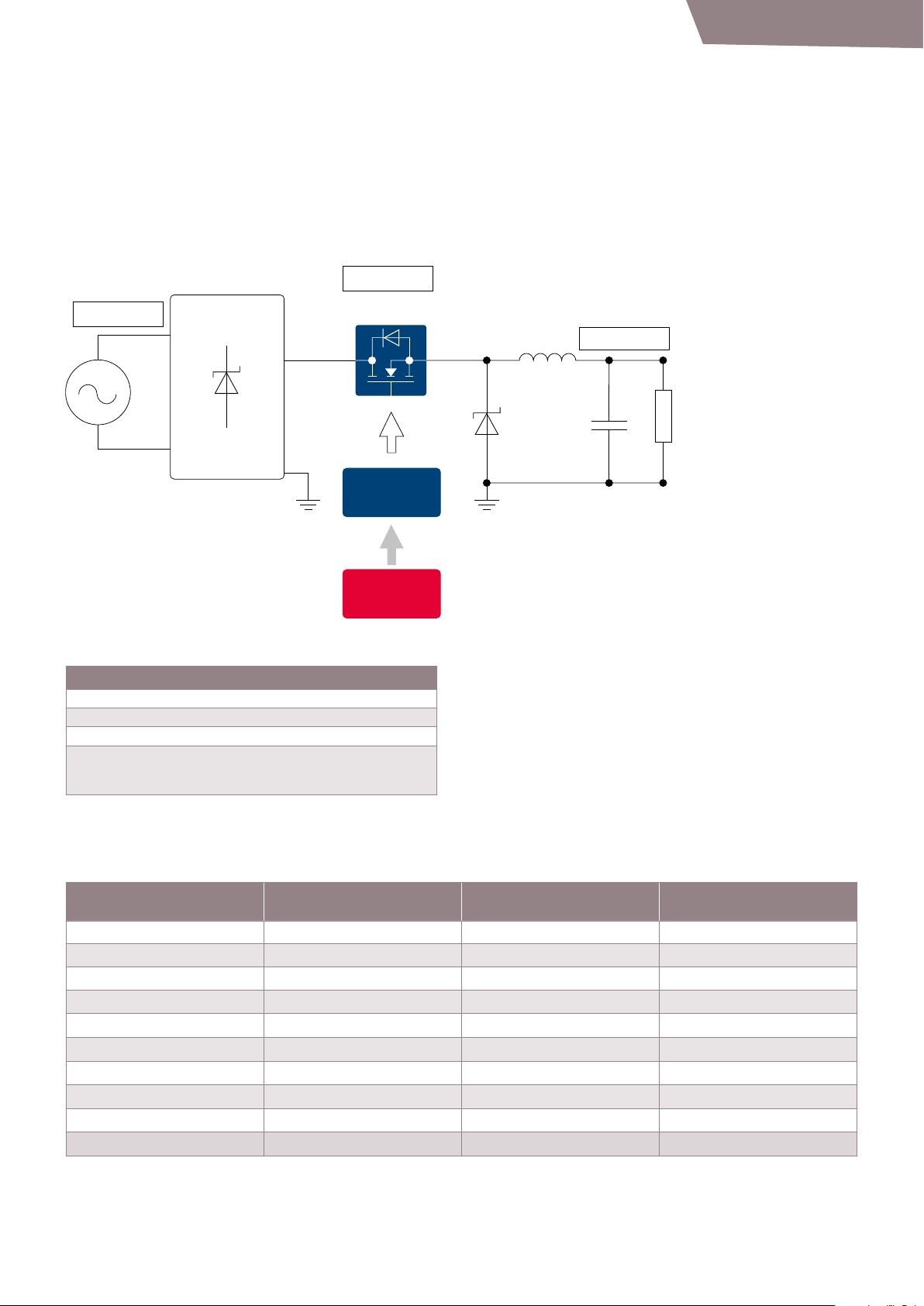
CoolMOS™ CE – overview
CoolMOS™ CE is a product family launched by Infineon to address consumer and lighting applications. It oers
benefits in eiciency and thermal behavior versus standard MOSFETs and has been optimized for ease-of-use and costcompetitiveness, while at the same time delivering state-of-the-art performance and Infineon quality and supply security.
Powered by Infineon multi-source program, CoolMOS™ CE is determined to support customers’ success in various consumer
markets by full FAE (field application engineer) support, short lead time and fast quote response.
CoolMOS™ quality - benchmark in short term and long
Potentially additional
defects reported in 2016
based on 130 million
0
2011 2012 2013 2014 2015
+
FIT rate < 0.15
device hours
term reliability
CoolMOS™ technology is legendary in the industry
dierentiated for its high quality, which has been proven
over the past years across billions of devices shipped with
continuous improved DPM down to less than 0.10 DPM.
Infineon has implemented firm and proven measures
from the beginning with design-for-quality program
and continuous improvement in production. There is
a constant proactive collaboration among technology,
design, quality, reliability and manufacturing teams to
achieve this result. This eort is above and beyond the
fact that all Infineon sites are ISO/TS16949 certified.
CoolMOS™ supply chain – delivery reliability, flexibility and supply security
Our customers value CoolMOS™ not only for its technical merits but also for the outstanding delivery reliability: once a
CoolMOS™ order date is committed, more than 96 percent of orders are shipped at or before the committed date. And
CoolMOS™ orders are committed to more than 80 percent to the date that the customers request. Security of supply and
flexibility to demand changes are focus targets and enabled by a well balanced production network. For example more than
90 percent of our products are qualified for production in at least two back end locations and more than 80 percent of the
volumes in two wafer fabs. This enables CoolMOS™ supply chain to react fast to changes in customer and market requirements.
Delivery reliability: ship date = committed date Delivery capability: confirm customers’ wish date
≥ 96% of CoolMOS™ orders are shipped by the committed date and ≥ 80% of wish dates can be met
4
Wish date
+1 week
+2 weeks
6%
4%
80%
www.infineon.com/ce
Page 5

Voltage range
This selection guide takes you to explore the advantages of CoolMOS™ CE in charger, adapter, TV and lighting applications
Soloreiust cone pratendeCoolMOS™ CE
CoolMOS™ CE
Charger
500 V
Product family and R
0.19 Ω – 3 Ω
600 V 650 V
range
DS(on)
0.19 Ω – 3.4 Ω 0.4 Ω – 1.5 Ω
Power supply topology and market segment
Adapter/charger
Quasi-resonant flyback
PC power
PFC/TTF 80+; PFC/LLC 90+
LCD TV
LLC half-bridge
LED retrofit/LED drivers
PFC/LLC/Non-isolated bulk
700 V
0.6 Ω – 2.1 Ω
LCD TV adapter
Quasi-resonant flyback
LED retrofit/LED drivers
Quasi-resonant flyback
800 V
0.31 Ω – 2.8 Ω
Reasons to choose CoolMOS™ CE
Non-technical benefits provided by CoolMOS™ CE
Product portfolio We own a broad portfolio covering five voltage classes in both through-hole and surface-mount packages.
Capacity We own the world’s largest capacity for power devices, with three dedicated frontends and four backends.
Thanks to factors such as the continued investment in our production facilities, we ensure a secure supply during a market
upswing.
Lead time We understand consumer and lighting market dynamics and oer a lead time for middle-sized orders of 4-6 weeks.
Delivery performance Our supply chain performance is constantly greater than or equal to 96 percent
(adhering to the customer committed date).
Quality Our field failure rates are as low as 0.1 PPM.
Design-in support We have a large field application engineering team dedicated to providing professional and flexible support for your design.
www.infineon.com/ce
5
Page 6
Ictam quodita dolorepChargers
10 W design: IPS65R1K5CE
15 W design: IPS65R1K0CE
Level [dBµV/m]
1G
Horizontal direction Vertical direction Horizontal direction Vertical direction
CoolMOS™ CE – smartphone and tablet chargers
Chargers for smartphones and tablets as well as other mobile applications demand for a growing output power at same
or smaller form factors, leading to increasing power density, and stringent requirements on thermal management, EMI
emissions and overall system cost. For example, many OEMs request a device temperature less than 90°C with an open
case and close case temperature less than 50°C.
Infineon recommends its series of 700 V CoolMOS™ CE superjunction MOSFETs for this application, which are used by
leading charger OEMs and design houses in their charger applications. Compared to planar MOSFETs the 700 V CoolMOS™
CE oers reduced switching and thus higher eiciency while passing EMI standards and ringing requirements. Several
reference designs have been developed by Infineon to help customers to simplify charger design and thus providing fast
time-to-market (see reference design selection table at end of section).
Value proposition of 700 V CoolMOS™ CE:
›
High eiciency, meeting application requirements
›
More than enough safety margin in thermals, for 10 W-25 W chargers
›
Good EMI performance – meets the EMI EN55022B standard without extra design-in eort
›
Easy-to-use product due to good controllability via gate resistor
›
Large breakdown voltage of nominal 700 V (and additional guard band typical) for safety on voltage spikes
Infineon recommends CoolMOS™ CE in 700 V for charger applications to secure suicient margin for voltage spikes.
CoolMOS™ CE products are also available in 650 V and 600 V for use in less sensitive designs.
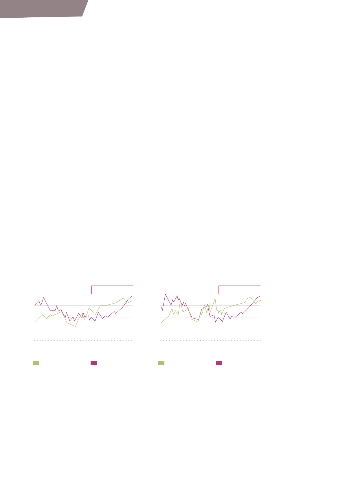
EN 55022 B radiated HF-field
30 MHz – 1 GHz position
40
30
20
10
0
-10
30M 50 60 80 100M
EN 55022 B RE 10 m OP EN 55022 B RE 10 m OP
200 300400 500 800 1G
Frequency [Hz]
40
30
20
10
Level [dBµV/m]
0
-10
30M 50 60 80 100M 200 300 400 500 800
EN 55022 B radiated HF-field
30 MHz – 1 GHz position
Frequency [Hz]
This figure shows the CoolMOS™ CE EMI performance in 10 W and 15 W charger applications. Maximum EMI limits are
indicated in the figure. CoolMOS™ CE could meet the EMI requirement thus oering design in flexibilities.
6
www.infineon.com/ce
Page 7
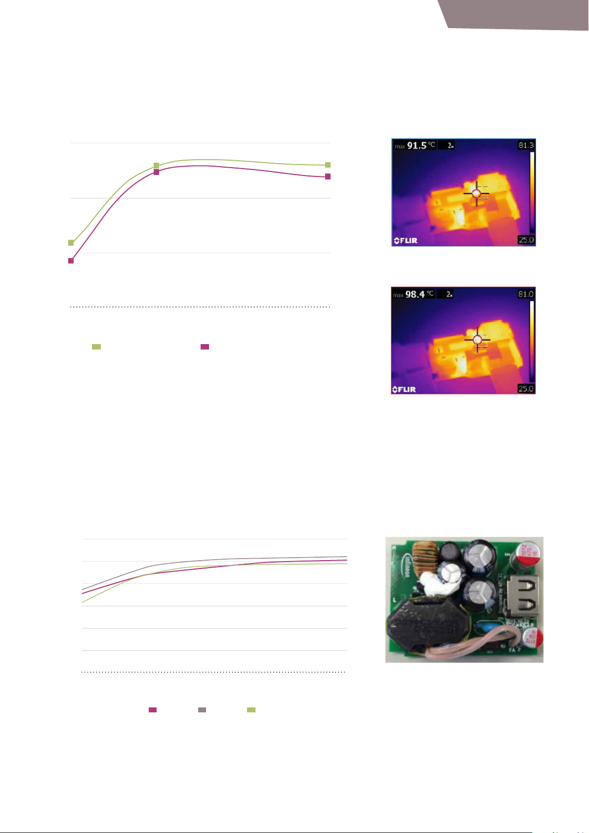
15 W QC 2.0 charger powered by IPS70R2K0CE IPS70R2K0CE
86
100
IPS70R2K0CE
Competitor 700 V, 1.6 Ω
Eiciency [%]
92
100
Eiciency [%]
5 V 9 V 12 V
Soloreiust cone pratendeChargers
85.19
84.98
85.22
84.80
84
82.32
82
81.73
Competitor 700 V, 1.6
80
25 50 75
Load [%]
Infineon CoolMOS™ CE oers higher eiciency and better thermals than planar MOSFETs: When replacing a 1.6 Ω planar
MOSFET with an Infineon 2.0 Ω CoolMOS™ CE in a 15 W QC 2.0 charger we measured ≥0.2 percent eiciency improvement. At the
same time, the MOSFET temperature was 7°C cooler, showing a clear benefit of using CoolMOS™ CE for charger applications.
Infineon’s 24 W QC 2.0 charger powered by IPS70R950CE Infineon’s 24 W quick charger
90
88
86
84
82
80
Also for 24 W quick chargers CoolMOS™ CE oers excellent eiciency, e.g., with the IPS70R950CE. Besides eiciency it
passes other spec requirements. The board is orderable through Infineon’s sample center.
www.infineon.com/ce
25 50 75
Load \[%]
DEMO_24W_QUICKCHARGER
7
Page 8
Ictam quodita dolorepChargers
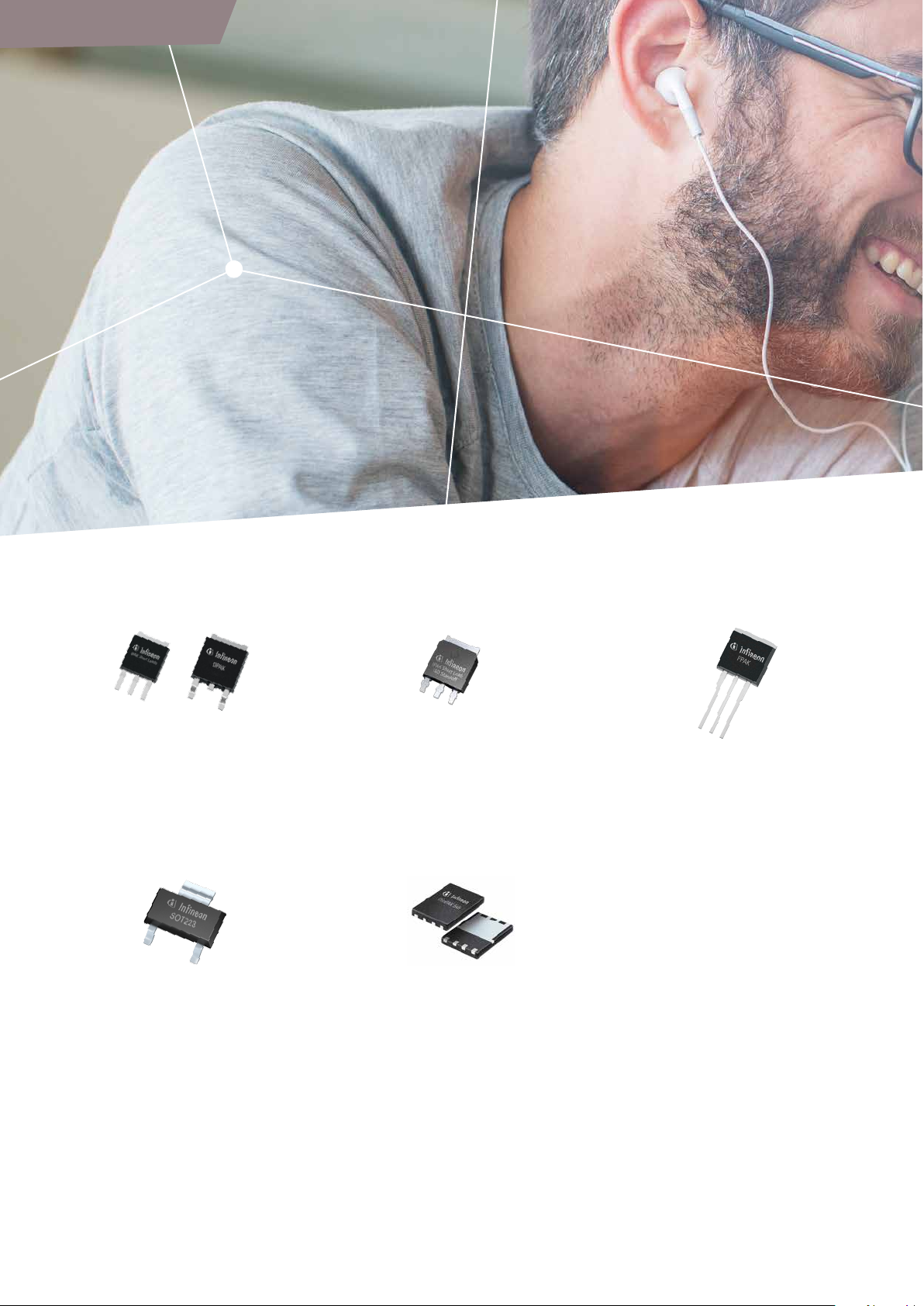
CoolMOS™ CE – package options for charger application
IPAK Short Lead and DPAK
Standard packages used in chargers
today with excellent reliability and
wide usage in the industry
SOT-223
Highly cost optimized surface-mount
package with small footprint. The
SOT-223 shows slightly worse thermal
performance than DPAK, however this
can be compensated with little eort
by oering a slightly larger copper
area (~15 mm²) around the package
for heatsinking on the PCB (see
page 14, lighting application)
IPAK Short Lead with
Isolation Stando:
Innovative package for charger
applications providing a defined
stando between package and PBC
ThinPAK 5x6
Very flat package (0.8 mm height)
package targeting slim charger
solutions. Bottom side cooling is
applied by many customers, but heat
sinking through the top side is also
possible
I2PAK
Larger package with better thermal
performance than IPAK short lead for
more than 20 W charger application.
The package carries higher cost yet
saves eorts in heat sinking
www.infineon.com/ce
8
Page 9

Soloreiust cone pratendeChargers
IPAK Short Lead with Isolation Stando
The new IPAK Short Lead with Mold Stopper will provide a defined stando
between package body and PCB for proper cleaning aer wave soldering to
avoid leakage current on board level. Mold bumps at the bottom of the package
body allow to fully insert the MOSFET into the PCB leaving a well-defined
isolation distance of 0.3 mm between the PCB and package body. Creepage
distance is increased and production yield is improved as area between
package and PCB can eectively be cleaned.
CoolMOS™ CE solutions for charger application
CoolMOS™ CE portfolio for charger – 700 V recommended for most designs
R
DS(on)
[m]
600 > 20
950/1000 18-25
1400/1500 10-18
2000/2100 < 10
General
proposal
[W] TO-262
(IPAK)
IPI70R950CE IPS70R950CE IPSA70R950CE IPD70R950CE IPN70R1K0CE
For 18 W-25 W charger Standard package
TO-251
(IPAK Short Lead)
IPS70R600CE IPSA70R600CE IPD70R600CE
IPS70R1K4CE IPSA70R1K4CE IPD70R1K4CE IPN70R1K5CE
IPS70R2K0CE IPSA70R2K0CE IPD70R2K0CE IPL70R2K1CES
for charger
TO-251
(IPAK Short Lead with
ISO Stando)
Standard package
for charger
TO-252
(DPAK)
For slim charger For slim charger Low cost/thermal
ThinPAK 5x6 SOT-223
adjustment needed
www.infineon.com/ce
9
Page 10
Ictam quodita dolorepNotebook adapters
DS
V
89.5
Eiciency [%]
Average eiciency
CoolMOS™ CE – notebook adapters
The CoolMOS™ CE series has been widely chosen by leading OEMs in notebook adapters. With ease-of-use, cost
competitiveness and short lead time as well as corresponding reference designs, customers can easily design CoolMOS™ CE
products in their adapters and have a faster time-to-market.
Value proposition of 600 V and 650 V CoolMOS™ CE for adapters
›
High eiciency exceeding values achieved with planar MOSFETs
›
Good thermals, especially for high density, small form factor designs
›
High breakdown voltage corridor – typical breakdown voltage by far exceeds specified max. value and is higher than
typical MOSFETs from other vendors
›
Easy-to-use product due to good controllability via gate resistor
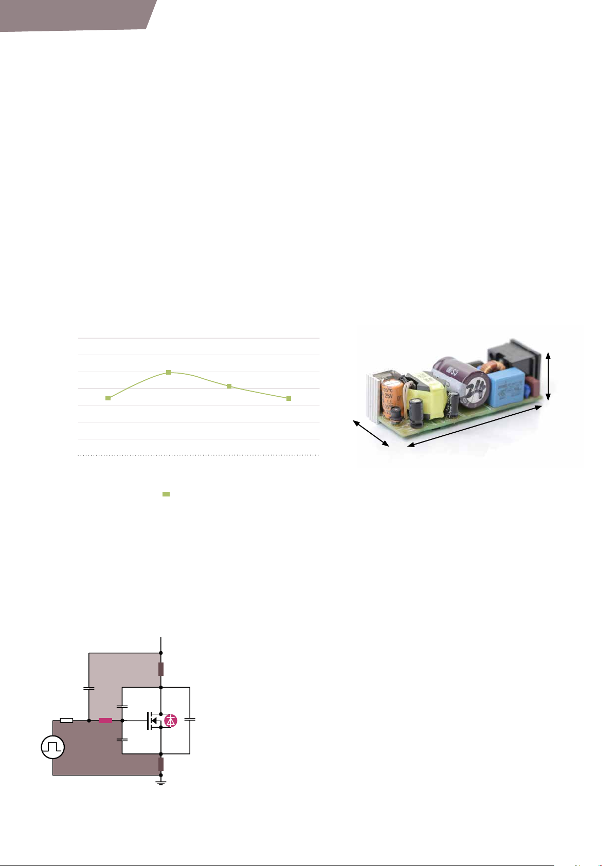
Infineon’s 35 W adapter powered by IPD60R650CE:
Active-mode eiciency versus AC line input voltage
Infineon’s 35 W adapter reference design has been powered by IPD60R650CE, which oers an eiciency of more than
87 percent and a peak power of 45 W for 2 ms. The dynamic load response is only ±2 percent and standby power is below
100 mW. Customers could modify this board according to their requirements, gaining time-to-market. The board is
orderable through Infineon’s sample center.
89.0
88.5
88.0
87.5
87.0
86.5
86.0
R
G,ext
Oscillation due to di/dt
88.72
Oscillation due to dV/dt
C
par
R
88.45
88.06
87.70
90 115 230 264
AC line input voltage [VAC]
Optimization for EMI and eiciency/thermals
EMI and eiciency/thermals need a careful trade-o in notebook adapters
DS
– better eiciency/thermals require faster switching, which leads to worse
EMI, e.g., due to the oscillations triggered by a high dV/dt (di/dt). With a small
L
C
GD
G
G,in
C
GS
par
D
S
L
source
adjustment this challenge can be overcome. We recommend our customers to
optimize EMI when designing-in high voltage superjunction MOSFETs by:
›
C
Adding additional drain-source capacitor CDS, e.g., 100 pF
›
Adjusting external RG, e.g., 5 Ω–30 Ω
›
Optimizing PCB layout for short path from controller to MOSFET gate and a
small loop inductance
›
Adjusting EMI filter (only if other measures are insuicient)
27 mm
35 mm 89 mm
REF-35W Adapter
10
www.infineon.com/ce
Page 11

Soloreiust cone pratendeNotebook adapters
Standard adapter
T
Narrow Lead
EMI optimization for a 45 W adapter
Radiation (db) in vertical direction
115 V
AC
IPA60R800CE -2.18* 187.78 -1.67* 186.22
Competitor A (planar MOS) -7.74* 120.13 -8.72 161.13
IPA60R800CE C
* Quasi-peak
: 100 pF -8.17* 182.24 -8.80* 183.28
DS
Frequency [MHz] 230 V
AC
Frequency [MHz]
The figure above shows a typical
Semi-slim adapter
example of adjusting EMI. It has been
done on a common 45 W adapter from
Slim adapter
the market, using a planar MOSFET.
Simply replacing the planar MOSFET
with IPA60R800CE leads to a worse
EMI performance. However, adding a
100 pF CDS significantly improves the
O-220 FullPAK TO-220 FullPAK
DPAK
EMI while meeting other specifications
such as eiciency, temperature, etc.
CoolMOS™ CE – Package options for notebook adapter application (35 W-65 W)
TO-220 FullPAK
Standard package used in
adapters today
TO-220 FullPAK Narrow Lead
Package for semi-slim adapter solution,
where height is smaller compared to
standard adapters. The legs of the
TO-220 FullPAK Narrow Lead package
have been modified with stando
height reduced from about 3.3 mm to
approximately 1.8 mm such that the
leads can be fully inserted into the PCB
without any production concerns. As a
result, MOSFET height is reduced while
creepage distance is preserved
DPAK
The DPAK solution has no concerns on
the package height for semi-slim and
slim adapter solutions, as its height
is far below the allowed height, and
it is on the other side of the package,
meaning space saving and power
density increasing, however better
thermal management is required
CoolMOS™ CE portfolio for 30 W to 65 W adapter
Voltage class
[V]
600
650
General proposal
R
DS(on)
[m]
400 IPA60R400CE IPD60R400CE
460 IPA60R460CE IPD60R460CE
650 IPA60R650CE IPD60R650CE IPAN60R650CE
800 IPA60R800CE IPD60R800CE IPAN60R800CE
400 IPA65R400CE IPD65R400CE
650 IPA65R650CE IPD65R650CE IPAN65R650CE
For standard adapter For slim adapter For semi-slim adapter
TO-220 FullPAK TO-252 DPAK TO-220 FullPAK Narrow Lead
www.infineon.com/ce
11
Page 12

Ictam quodita dolorep
95
Eiciency [%]
TV sets
CoolMOS™ CE – TV sets
CoolMOS™ CE oers a wide range of products for the TV SMPS application and is selected by the world’s leading TV manufacturers
due to high quality, reliability and ease-of-use. Together with XDP™ digital power, OptiMOS™, EiceDRIVER™ and other components
from Infineon, we oer system solutions as demonstrated by a wide range of reference designs. Our dedication for TV application has
been further demonstrated by developing 600 V CoolMOS™ CE in TO-220 FullPAK Wide Creepage products mainly for TV application.
Value proposition of 500 V, 600 V, 650 V and 700 V CoolMOS™ CE for TV applications:
For the AC-DC power supply in TV applications, CoolMOS™ CE devices come in dierent voltage classes of 500 V, 600 V, 650 V
and 700 V so as to be used in both PFC and LLC stages. The CoolMOS™ CE devices are oered in dierent packages such as TO-220
FullPAK, TO-220 FullPAK Wide Creepage, DPAK and SOT-223. This variety enables customer to use these packages in dierent stages
of the power supply to ease the PCB layout design and manufacturing. As an example, the TO-220 FullPAK can be used in the topside PFC stage and the DPAK or SOT-223 can be used in the bottom side LLC stage making the layout simpler, and eiciently meeting
the thermal and EMI requirements. When CoolMOS™ CE devices are driven with optimal gate driving techniques, they exhibit low
temperature rise and provide high eiciency performance. These devices are robust and are capable of withstanding higher stress
under fault conditions. This high reliability feature makes them suitable for operation in environments which have unstable power
conditions. As an example, the stress on the PFC MOSFETs can be high under input line transient or faulty load conditions. The
CoolMOS™ CE devices safely carry high peak currents until the PWM controller responds to the transient condition.
Infineon’s 120 W TV SMPS design powered by IPD60R400CE and IPD60R1K5CE
Infineon oers a reference design for a 120 W TV SMPS which combines the advantages of XDP™ digital power and
CoolMOS™ CE to oer the state-of-the-art performance, where IDP2302 is used to control system, and IPD60R400CE and
IPD60R1K5CE are used in the PFC and LLC stages respectively. It is a slim design and cost optimized for customers.
CoolMOS™ CE portfolio for TV
91
87
83
79
75
Voltage class
[V]
R
DS(on)
[m]
190
280
800
400/380
500/460
650/600
950/1000
1500/1400
General
proposal
150 mm
200 mm
30 60 90 120
Load [W]
90 V
AC
TO-220 FullPAK TO-252
IPA50R190CE IPAW60R190CE
IPA50R280CE IPD50R280CE IPAW60R280CE
IPA50R800CE IPD50R800CE IPA60R800CE IPD60R800CE
IPA50R380CE IPD50R380CE IPA60R400CE IPD60R400CE IPAW60R380CE IPA65R400CE IPD65R400CE
IPA50R500CE IPD50R500CE IPA60R460CE IPD60R460CE
IPA50R650CE IPD50R650CE IPA60R650CE IPD60R650CE IPAW60R600CE IPA65R650CE IPD65R650CE IPAW70R600CE
IPA50R950CE IPD50R950CE IPA60R1K0CE IPD60R1K0CE IPA65R1K0CE IPD65R1K0CE IPAW70R950CE
PFC: 190 mΩ – 600 mΩ
LLC: 400 mΩ – 1500 mΩ
110 V
AC
500 600 650 700
(DPAK)
IPD50R1K4CE IPA60R1K5CE IPD60R1K5CE IPA65R1K5CE IPD65R1K5CE
230 V
AC
TO-220 FullPAK TO-252
PFC: 190 mΩ – 600 mΩ LLC: 400 mΩ – 1500 mΩ
265 V
AC
(DPAK)
Flyback: 400 mΩ – 1500 mΩ
TO-220 FullPAK
Wide Creepage
DEMO-IDP2302-120W
TO-220 FullPAK TO-252
(DPAK)
Flyback: 400 mΩ – 1500 mΩ Flyback
TO-220 FullPAK
Wide Creepage
www.infineon.com/ce
14 mm
12
Page 13

Soloreiust cone pratende
10.6
16.013.7
11.3
2.3
TV sets
New TO-220 FullPAK Wide Creepage package for CoolMOS™
TO-220 FullPAK
standard
3.3
2.54
Wider creepage for applications
susceptible to pollution
TO-220 FullPAK
The
to increase creepage distance: the application of potting, the usage of sleeves, pre-bending of leads and other
workarounds come at an extra cost of estimated 2-5 USD cents. This cost and the additional process steps can be
removed with the Wide Creepage package.
Wide Creepage reduces system cost by oering an alternative to frequently used approaches
TO-220 FullPAK
Wide Creepage
16.313.2
4.25
The TO-220 FullPAK Wide Creepage increases the creepage distance
to 4.25 mm compared to 2.54 mm for a standard TO-220 package. It
fully meets requirements of the EN60664-1 standard that requires
at least 3.6 mm for open frame electrical power supplies which are
oen found in LED TV, PC power or industrial power supplies: in these
applications, air vents in the external casing to allow some air flow
which will assist in cooling the internal components. This makes
the inside susceptible to pollutants such as dust particles. These
pollutants reduce the eective creepage between pins. High voltage
arcing can destroy the MOSFET used in SMPS when the pollutants
reduce the eective creepage distance.
Benefits
›
Wide creepage of 4.25 mm to avoid arcing even in polluted environment
›
Cost savings of 2-5 USD cent in creepage protection by removing additional process steps
›
Fully automated PCB assembly eliminating process variation
›
FullPAK benefit of isolation, lower package capacitances, lower EMI
CoolMOS™ CE oers 500 V, 600 V, 650 V and 700 V products in TO-220 FullPAK, TO-252 (DPAK) and TO-220 FullPAK Wide
Creepage for TV SMPS solutions. For the PFC section 500 V/600 V products with an R
preferred. We recommend 400 mΩ to 1500 mΩ 500 V/600 V products in the LLC section. For flyback 400 mΩ to 1500 mΩ
600 V/ 650 V parts are recommended for customer design.
www.infineon.com/ce
between 190 mΩ and 600 mΩ are
DS(on)
13
Page 14

Ictam quodita dolorepLighting
3.5
6.5
CoolMOS™ CE for lighting applications
Good eiciency, ease-of-use and EMI performance at an attractive cost position make the CoolMOS™ CE series the product of choice for LED drivers or LED tubes in buck, flyback, PFC and LLC topology. Its benefits include an improvement in
eiciency and thermal behavior compared to standard MOSFETs.
CoolMOS™ products aimed at lighting bring the benefits of highest quality and delivery reliability as outlined in the overview section for the CoolMOS™ portfolio. However, the CoolMOS™ CE series has been defined with a particular focus on the
customers’ needs, for an attractive price and fastest supply availability.
CoolMOS™ CE in SOT-223 package
With the rapid conversion from CFL to LED lighting, customer requirements are rapidly changing: On the one hand, power
levels are further decreasing, while on the other hand, increasing cost pressure compels power designers to optimize designs to a fraction of a cent. The completion of the CoolMOS™ CE portfolio with the SOT-223 package is Infineon’s answer to
this challenge: It facilitates a further reduction in BOM cost – and additional footprint optimization in some designs – with
only a minor compromise in terms of thermal behavior.
SOT-223 as drop-in replacement for DPAK at a lower cost
The SOT-223 package with a decapped middle pin is fully compatible with the footprint of a DPAK, therefore allowing
one-on-one drop-in replacements and second sourcing.
DPAK SOT-223
6.2
6.7
6.5
3.5
14
www.infineon.com/sot-223
Page 15

Soloreiust cone pratendeLighting
T [°C]
P
= 250 mW
Thermal behavior – on a par with DPAK
The thermal behavior of the SOT-223 primarily depends on the layout of the board where the package is used and on the
power consumed. We have measured the thermals in a test environment and compared them with a simulation. Compared to a DPAK positioned on a typical DPAK footprint, the SOT-223 displays the following thermal behavior:
70
65
60
55
57.8
DPAK on DPAK
footprint (reference)
loss
68.0
+10°C
SOT-223 on SOT-223
footprint
Good for low
›
power levels
Footprint savings
›
vs. DPAK
62.8
+5°C
SOT-223 on DPAK
footprint
Drop-in replacement
›
for DPAK
Good for designs
›
with thermal margin
Recommended use case
59.8
+2°C
SOT-223 on footprint
of DPAK + 20 mm
Replacement for DPAK
›
Good for designs
›
with suicient
cooling area
2
Cu
›
Same footprint as DPAK – when mounted on a standard DPAK footprint, the SOT-223 package shows a temperature
elevated by 4–5 K. This behavior makes the SOT-223 suitable for designs with a thermal margin
›
Footprint of DPAK plus ~20 mm2 additional copper area – in many designs, the MOSFET is mounted on a larger
Cu area which serves as a heatsink embedded in the PCB. As soon as 20 mm2 Cu or more is available in addition to the DPAK
footprint, the temperature increase is no more than 2–3 K above DPAK and the SOT-223 can be used as a drop-in replacement
›
SOT-223 on SOT-223 footprint – when mounted on the SOT-223 footprint without an additional surrounding Cu area, the
package leads to a 10 °C temperature increase compared to a DPAK. This means that the option of space savings via the
SOT-223 is only useful for very low power applications
www.infineon.com/sot-223
15
Page 16

Ictam quodita dolorepLighting
footprint ~40 mm
Min. SO
footprint
350
Simulation result: P
= 250 mW, T
= 70°C, board 76 x 114 mm
Thermal behavior – on a par with DPAK
100
B
95
90
85
[°C]
j
T
80
75
70
65
T-223
loss
98°C
C
A
85°C
0
D
50 100
Standard DPAK
amb
SOT-223 slightly higher temperature on
DPAK standard footprint – ∆T ~ 4–5°C
Same thermal performance of SOT-223 as
DPAK with a Cu footprint of ~60 mm
(increase of ~20 mm2 board space)
+4°C
150 200
2
Cu area [mm
2
SOT-223
DPAK
2
]
250 300
The laboratory findings on thermal behavior are confirmed by a thermal simulation with T
= 70°C and P
ambient
= 250 mW.
loss
The size of the copper area in the footprint is shown on the x-axis, while the y-axis displays the temperature of the package top side. In the case of an SOT-223 on DPAK footprint, the 4–5 K temperature increase over DPAK is confirmed. But
when used in conjunction with an enlarged copper area of ~20 mm2, a temperature increase of 2–3 K is measured.
CoolMOS™ CE SOT-223 product portfolio
R
[m] 500 V 600 V 650 V 700 V
DS(ON)
3400 IPN60R3K4CE
3000 IPN50R3K0CE
2000/2100 IPN50R2K0CE IPN60R2K1CE
1400/1500 IPN50R1K4CE IPN60R1K5CE IPN65R1K5CE IPN70R1K5CE
950/1000 IPN50R950CE IPN60R1K0CE IPN70R1K0CE
800 IPN50R800CE
650 IPN50R650CE
www.infineon.com/sot-223
16
Page 17

CoolMOS™ CE – demonstrator boards
Soloreiust cone pratendeDemonstrator boards
ICL8201 demoboard with 500 V CoolMOS™
End application: 5 W-10 W LED lamp
Parameter Value
Output power 7.5 W
Input voltage 90 V
Frequency 50 Hz/60 Hz
Power factor > 0.95 at low line
THD < 20% at low line
Eiciency 85%
Output voltage 33 V
Output current 180 mA
Infineon order code
1)
–265 V
AC
AC
> 0.80 at high line
< 30% at high line
–47 V
DC
DC
EVALLEDICL8201F1 / SP001339448
ICL5101 demoboard with 600 V CoolMOS™
2)
End applications: indoor and outdoor high power LED lighting,
high-bay and low-bay lighting, street lighting, parking garages
and area lighting, oice panel and shop lighting
Parameter Value
Output power 110 W
Input voltage 85 V
Output voltage 54 V
Output current 2060 mA
Eiciency ~ 94%
Power factor > 99%
THD < 10%
TAmbient 80°C–100°C
Infineon order code
1)
–305 V
AC
AC
DC
EVALLEDICL5101E1 / SP001296078
ICL8201 demoboard with 650 V CoolMOS™
End application: Single end cap T8 form factor LED lamp
Parameter Value
Output power 18 W
Input voltage 170 V
Frequency 50 Hz
Power factor > 0.95
THD < 20%
Eiciency > 90%
Output voltage 55 V
Output current 270 mA
Infineon order code
1)
Go to our website for more specific information about the demoboard
2)
Also suitable for 500 V due to excellent V
3)
Launch in 09/2016, higher eiciency and lower price
1)
–277 V
AC
AC
–75 V
DC
DC
EVALLEDICL8201F2 / SP001339450
regulation and error protection
bulk
ICL8105 demoboard with 800 V CoolMOS™
End application: Electronic control gear
for LED luminaires (20 W–80 W)
Parameter Value
Output power 40 W
Nominal input voltage 90 V–300 V~
Input overvoltage 310 V~
Output voltage 15 V–45 V
Output overvoltage threshold 50 V
Output current 880 mA
Eiciency <91%
Power factor >0.95
THD
Infineon order code:
20 W-80 W version:
1)
<16%
EVALLEDICL8105F2 / SP001296076
EVALLEDICL8105E1 / SP001296074
3)
www.infineon.com/ce
17
Page 18

Ictam quodita dolorepTarget topologies
CoolMOS™ CE – target topologies
Single switch topologies – boost/PFC
Typically used in high power adapters, PC power, TV power supplies front-end
PFC stage
MOSFET driver
Digital/analog controller
Design equations for MOSFET selection
= V
V
DS
out
ID = I
* 1 / (1-D)
out
= 1.5 * VDS (with derating for all variables on board)
V
DS_FET
max. 25°C for acceptable power dissipation in MOSFET package
R
DS(on)
= (1.5 * P
case operation conditions. Ipk = 1.5 * I
P
device
) / (Ipk² * D). Ipk is derated value of ID to cover all worst
device
= (Tj – Ta) / R
thJA
D
400 V at 0.5 A
18
* Two in parallel
Output power
[W]
200 85 V
150 85 V
100 85 V
75 85 V
Input voltage
[V]
…265 V
AC
…265 V
AC
…265 V
AC
…265 V
AC
PFC output load current at 400 V
output voltage
CoolMOS™ CE
device options
[A]
AC
AC
AC
AC
0.60 IPx60R400CE*
0.40 IPx60R460CE
0.30 IPx60R650CE
0.20 IPx60R800CE
www.infineon.com/ce
Page 19

CoolMOS™ CE – target topologies
Quasi-resonant flyback topologies
Typically used in chargers, adapters, auxiliary power supplies
Soloreiust cone pratendeTarget topologies
PFC stage
MOSFET driver
Digital/analog controller
Design equations for MOSFET selection
= Vin + VR, where VR = (0.8 * V
V
DS
= Vin * ton / L
I
D
V
DS_FET
R
DS(on)
= (1.5 * P
case operation conditions. Ipk = 1.5 * I
P
= (Tj – Ta) / R
device
p
= 1.5 * VDS (with derating for all variables on board)
max. 25°C for acceptable power dissipation in MOSFET package
) / (Ipk² * D). Ipk is derated value of ID to cover all worst
device
thJA
* (NP / NS))
out
D
Snubber/
active clamp
MOSFET driver
PWM/QR stage - flyback
12 V at 3 A
Isolation
Selection is based for 85 V
to 265 VAC input voltage,
AC
100 kHz switching frequency. Reflected voltage (VR) design greatly aects MOSFET VDS selection criteria. Mode
of operation – CCM (continuous conduction mode) or
DCM (discontinuous conduction mode) also aects
MOSFET R
selection criteria.
DS(on)/ID
Output
power
[W]
120 19 6 71 143 IPx65R650CE IPx65R650CE
100 24 5 107 214 IPx65R650CE IPx65R1k0CE
75 19 6 107 214 IPx65R650CE IPx65R1k0CE
50 12 10 107 214 IPx65R650CE IPx65R1k0CE
36 12 10 143 286 IPx70R600CE IPx70R1K4CE
25 9 13 143 286 IPx70R950CE IPx70R1K4CE
15 5 24 143 286 IPx70R950CE IPx70R1K4CE
10 5 24 214 429 IPx70R1K4CE IPx70R1K4CE
5 5 24 429 857 IPx70R2K0CE IPx70R1K4CE
www.infineon.com/ce
Output
voltage
[V]
Turns ratio
NP/NS
Primary
inductance
DCM
[uH]
Primary
inductance
CCM
[uH]
CoolMOS™ CE
device options
DCM
CoolMOS™ CE
device options
CCM
19
Page 20

Ictam quodita dolorepTarget topologies
CoolMOS™ CE – target topologies
Wide input range flyback topologies
Typically used in LED drivers and adapters
90 Vto 300 V
AC AC
Bridge rectifier
Digital/analog controller
Design equations for MOSFET selection
= V
+ VR, where VR = (0.8 * V
V
DS
in
= Vin * ton / L
I
D
V
DS_FET
max. 25°C for acceptable power dissipation in MOSFET pack-
R
DS(on)
age = (1.5 * P
case operation conditions. Ipk = 1.5 * I
P
= (Tj – Ta) / R
device
p
= 1.5 * VDS (with derating for all variables on board)
) / (Ipk² * D). Ipk is derated value of ID to cover all worst
device
thJA
* (NP / NS))
out
D
Snubber/
active clamp
MOSFET driver
PWM/QR stage - flyback
Isolation
Selection is based for 85 VAC to 300 VAC input voltage,
100 kHz switching frequency. Reflected voltage (VR) design
aects MOSFET VDS selection criteria. 800 V devices allow
greater VR range. Mode of operation – CCM (continuous
conduction mode) or DCM (discontinuous conduction
mode) also aects MOSFET R
selection criteria.
DS(on)/ID
5 V at 3 A
20
Output
power
[W]
Output
voltage
[V]
Turns ratio
NP/NS
Primary
inductance
DCM
[uH]
Primary
inductance
CCM
[uH]
CoolMOS™ CE
device options
DCM
CoolMOS™ CE
device options
CCM
150 24 5 71 143 IPA80R310CE IPA80R460CE
100 24 5 107 214 IPA80R310CE IPA80R650CE
50 12 10 107 214 IPA80R310CE IPA80R650CE
36 12 10 143 286 IPA80R460CE IPA80R1K0CE
25 9 13 143 286 IPA80R460CE IPA80R1K0CE
15 5 24 143 286 IPA80R460CE IPA80R1K0CE
10 5 24 214 429 IPA80R650CE IPA80R1K4CE
5 5 24 429 857 IPA80R1K0CE IPx80R2K8CE
www.infineon.com/ce
Page 21
CoolMOS™ CE – target topologies
Single switch topologies – buck
Typically used in LED drivers, motor controllers, high power adapters, TV power supplies front-end
Buck
to 265 V
85 V
AC AC
24 V at 2 A
Soloreiust cone pratendeTarget topologies
Design equations for MOSFET selection
= V
V
DS
in
ID = I
out
V
= 1.5 * VDS (with derating for all variables on board)
DS_FET
max. 25°C for acceptable power dissipation in MOSFET package
R
DS(on)
= (1.5 * P
case operation conditions
) / (Ipk² * D). Ipk is derated value of ID to cover all worst
device
Input voltage
Output load current
[V]
110 V
AC
110 V
AC
85 V
…265 V
85 V
85 V
85 V
85 V
85 V
85 V
85 V
AC
AC
AC
AC
AC
AC
AC
AC
…265 V
…265 V
…265 V
…265 V
…265 V
…265 V
…265 V
AC
AC
AC
AC
AC
AC
AC
AC
[A]
Driver
Microcontroller
Output power
[W]
CoolMOS™ CE
device options
7 200 IPx50R190CE*
6 180 IPx50R280CE*
5 150 IPx60R400CE
4 120 IPx60R460CE
4 100 IPx60R650CE
3 75 IPx60R650CE
3 50 IPx60R1k0CE
2 25 IPx60R1k5CE
2 10 IPx60R2k1CE
1 5 IPx60R3k4CE
* Two in parallel
www.infineon.com/ce
21
Page 22

Ictam quodita dolorepTarget topologies
CoolMOS™ CE – target topologies
Two switch topologies – half-bridge LLC
Typically used in PC power and TV power supplies
The ideal MOSFET for the LLC converter would allow for zero dead time (maximum power transfer) and no conduction
loss. Hence selecting a lower R
appropriate MOSFET QG, Q
caused by E
can be considered negligible, and to this extent, E
oss
oss
MOSFET will help lower condition losses. Since LLC operates fully in ZVS-mode (given
DS(on)
, selected Q
and m-values – and ample pre-programmed deadtime), switching loss
max
is not a critical MOSFET parameter for LLC.
oss
From PFC
output
Half-bridge driver
Digital/
analog controller
Design equations for MOSFET selection
= V
V
DS
in
ID = I
* (NS / NP)
out
= 1.5* VDS (with derating for all
V
DS_FET
variables on board)
max. 25°C for acceptable power
R
DS(on)
dissipation in MOSFET package = (1.5 * P
(Ipk² * D). Ipk is derated value of ID to cover all
worst case operation conditions
device
LLC half-bridge
Isolation
12 V at 10 A
In LLC topology, the MOSFET body diode could potentially experience hard
current commutation in abnormal conditions, if steps are not taken specifically to avoid this either by a good control scheme or additional circuitry in the
topology. The CoolMOS™ CE addresses the potential issue of reverse recovery of
body diode by employing a self-snubbing scheme causing the channel to partial-
) /
ly turn on at high dV/dt (induced by C
voltage divider) in order to prevent
GD/CGS
avalanche breakdown, thus providing the extra measure of protection during
hard body diode commutation.
22
Input voltage
VDC [V]
400 250 24 128 109 356 20 IPx60R400CE IPx50R380CE
400 200 24 160 136 445 16 IPx60R460CE IPx50R500CE
400 150 24 213 181 594 12 IPx60R650CE IPD50R650CE
400 100 24 320 272 890 8 IPx60R800CE IPD50R800CE
400 75 24 427 363 1187 6 IPx60R1k0CE IPD50R950CE
Output
voltage
[V]
Output volt-
age Vo [V]
Rac
[]
Lr
[uH]
Lp
[uH]
Cr
[nF]
600 V
CoolMOS™ CE
device
options
CoolMOS™ CE
www.infineon.com/ce
500 V
device
options
Page 23

Soloreiust cone pratendeSoloreiust cone pratende
Infineon support for high voltage MOSFETs
Useful links and helpful information
Further information, datasheets and documents
www.infineon.com/ce
›
www.infineon.com/coolmos
›
www.infineon.com/coolmos-500V
›
www.infineon.com/coolmos-600V
›
Videos
www.infineon.com/mediacenter
›
Simulation
www.infineon.com/coolmos-650V-700V
›
www.infineon.com/coolmos-800V
›
www.infineon.com/powermosfet-simulationmodels
›
23
Page 24

Ictam quodita dolorepProduct portfolio
500V CoolMOS™ CE
R
DS(on)
[mΩ]
190
280 IPP50R280CE IPA50R280CE IPW50R280CE IPD50R280CE
380
500 IPP50R500CE IPA50R500CE IPAN50R500CE IPD50R500CE
650 IPA50R650CE IPD50R650CE IPN50R650CE
800 IPA50R800CE IPD50R800CE IPN50R800CE
950 IPA50R950CE IPD50R950CE IPU50R950CE IPN50R950CE
1400 IPD50R1K4CE IPU50R1K4CE IPN50R1K4CE
2000 IPD50R2K0CE IPU50R2K0CE IPN50R2K0CE
3000
TO-220 TO-220 FullPAK
IPP50R190CE IPA50R190CE IPW50R190CE
IPP50R380CE IPA50R380CE IPD50R380CE
600V CoolMOS™ CE
R
DS(on)
[mΩ]
190
280 IPAW60R280CE
380 IPAW60R380CE
400 IPA60R400CE IPD60R400CE IPS60R400CE
460 IPA60R460CE IPD60R460CE IPS60R460CE
600 IPAW60R600CE
650 IPA60R650CE IPAN60R650CE IPD60R650CE IPS60R650CE
800 IPA60R800CE IPAN60R800CE IPD60R800CE IPS60R800CE
1000 IPA60R1K0CE IPD60R1K0CE IPU60R1K0CE IPS60R1K0CE IPN60R1K0CE
1500
2100 IPD60R2K1CE IPU60R2K1CE IPS60R2K1CE IPN60R2K1CE
3400 IPD60R3K4CE IPU60R3K4CE IPS60R3K4CE IPN60R3K4CE
TO-220 FullPAK
IPA60R1K5CE IPD60R1K5CE IPU60R1K5CE IPS60R1K5CE IPN60R1K5CE
650V CoolMOS™ CE
R
DS(on)
[mΩ]
400 IPA65R400CE IPD65R400CE IPS65R400CE
650
1000 IPA65R1K0CE IPD65R1K0CE IPS65R1K0CE
1500 IPA65R1K5CE IPD65R1K5CE IPS65R1K5CE IPN65R1K5CE
TO-220 TO-220 FullPAK
700V CoolMOS™ CE
R
DS(on)
[mΩ]
600
950
1000
1400
1500
2000
2100
TO-220
ACTIVE & PREFERRED
ACTIVE & PREFERRED
TO-220 FullPAK
Wide Creepage
IPAW60R190CE
ACTIVE & PREFERRED
IPA65R650CE IPAN65R650CE IPD65R650CE IPS65R650CE
ACTIVE & PREFERRED
TO-220 FullPAK
Wide Creepage
IPAW70R600CE IPD70R600CE IPSA70R600CE IPS70R600CE
IPAW70R950CE IPI70R950CE IPD70R950CE IPSA70R950CE IPS70R950CE
TO-220 FullPAK
Narrow Lead
TO-220 FullPAK
Narrow Lead
TO-220 FullPAK
Narrow Lead
TO-262
(I2PAK)
TO-247
TO-252
(DPAK)
IPD50R3K0CE IPU50R3K0CE IPN50R3K0CE
TO-251
(IPAK)
TO-252
(DPAK)
TO-252
(DPAK)
TO-252
(DPAK)
IPD70R1K4CE IPSA70R1K4CE IPS70R1K4CE
IPN70R1K5CE
IPD70R2K0CE IPSA70R2K0CE IPS70R2K0CE
TO-251
(IPAK Short Lead
with ISO Stando)
TO-251
(IPAK)
TO-251
(IPAK)
TO-251
(IPAK Short Lead)
(IPAK Short Lead)
(IPAK Short Lead)
TO-251
(IPAK Short Lead)
TO-251
TO-251
SOT-223 ThinPAK 5x6
IPN70R1K0CE
IPL70R2K1CES
SOT-223
Charger
SOT-223
SOT-223
Charger
Charger
800V CoolMOS™ CE
R
DS(on)
[mΩ]
310
460 IPA80R460CE
650 IPA80R650CE
1000 IPA80R1K0CE IPD80R1K0CE IPU80R1K0CE
1400 IPA80R1K4CE IPD80R1K4CE IPU80R1K4CE
2800
24
ACTIVE
TO-220 TO-220 FullPAK TO-247
IPA80R310CE
TO-252
(DPAK)
IPD80R2K8CE IPU80R2K8CE
TO-251
(IPAK)
TO-251
(IPAK Short Lead)
www.infineon.com/ce
Page 25

Soloreiust cone pratendePackage overview
CoolMOS™ CE portfolio package overview
Package Vol-
SOT-223
TO-247 500
IPAK
IPAK Short Lead
IPAK Short Lead with
ISO Stando
DPAK
IPAK 700
TO-220 FullPAK
TO-220 Standard 500
TO-220 FullPAK Narrow Lead
TO-220 FullPAK Wide Creepage
ThinPAK 5x6 700
tage
[V]
500 650/800 950/1400 2000/3000
600 1000/1500 2100/3400
650 1500
700
600
800
600
650
700
700
500
600
650
700
800
500
600 400 460 650/800 1000/1500
650 400 650 1000/1500
800
500
600
650
600
700
0-59 60-89 90-149 150-199 200-299 300-400 401-600 601-899 900-1500 >1500
190 280
190 280 380 500 650/800 950
190 280 380 500
190 280 380 600
R
[m]
DS(on)
1000/1500
1000/1500 2100
1000/1400 2800
400 460 650/800 1000/1500 2100/3400
400 650 1000/1500
600 950/1400 2000
600 950/1400 2000
280 380 500 650/800 950/1400 2000/3000
400 460 650/800 1000/1500 2100/3400
400 650 1000/1500
600 950/1400 2000
1000/1400 2800
950
310 460 650 1000/1400
500
650/800
650
600
950
2100
ACTIVE & PREFERRED ACTIVE
www.infineon.com/ce
25
Page 26
Ictam quodita dolorepCross reference
500 V CoolMOS™ CE
CoolMOS™ CE
IPA50R950CE
IPA50R800CE
IPA50R650CE
IPA50R500CE
IPA50R380CE
IPA50R280CE
IPA50R190CE
IPP50R500CE
IPP50R380CE
IPP50R280CE
IPP50R190CE
IPD50R3K0CE
IPD50R2K0CE
IPD50R1K4CE
IPD50R950CE
IPD50R800CE
IPD50R650CE
IPD50R500CE
IPD50R380CE
IPD50R280CE
IPU50R3K0CE
IPU50R2K0CE
IPU50R1K4CE
IPU50R950CE
IPW50R280CE
IPW50R190CE
Superjunction MOSFET Planar MOSFET
STMicroelectronics
STF8NM50N AOTF8T50P SiHFI840G
STF10NM50N
STF11NM50N AOTF12N50 SiHFIB7N50A FMV12N50E
STF19NM50N SiHF18N50D FMV20N50E
STF23NM50N
STP11NM50N SiHP12N50C FMP12N50E
STP12NM50 SiHP12N50E FMP16N50E
STP19NM50N SiHP15N50E FMP20N50E
STP23NM50N SiHP20N50E
STD8NM50N AOD9N50
STD10NM50N
STD11NM50N
STD14NM50N SiHD12N50E
STW19NM50N AOK22N50 SiHG460B
STW23NM50N SiHFP31N50L
Alpha and Omega
Semiconductor
AOTF14N50 SiHF16N50C FMV16N50E
AOD3N50 SiHFR420 TK3P50D
AOD6N50 SiHD5N50D TK5P50D
AOU3N50 SiHFU420
Vishay Fuji Electric Toshiba
FMV08N50E
SiHF8N50D
FMV12N50ES
FMV16N50ES
FMV21N50ES
FMP12N50ES
FMP16N50ES
FMP20N50ES
SiHU5N50D CS830 A3RD SVF830M MDIS5N50TH
TK12A50D
TK13A50D
TK18A50D
TK7P50D
600 V CoolMOS™ CE
CoolMOS™ CE
IPA60R1K5CE
IPA60R1K0CE
IPA60R800CE
IPA60R650CE
IPA60R460CE
IPA60R400CE
IPD60R3K4CE
IPD60R2K1CE
IPD60R1K5CE
IPD60R1K0CE
IPD60R800CE
IPD60R650CE
IPD60R460CE
IPD60R400CE
IPU60R3K4CE
IPU60R2K1CE
IPU60R1K5CE
IPU60R1K0CE
IPS60R3K4CE
IPS60R2K1CE
IPS60R1K5CE
IPS60R1K0CE
IPS60R800CE
IPS60R650CE
IPS60R460CE
IPS60R400CE
Semiconductor
FCPF600N60Z STF10NM60N STF10N60M2 TK7A60W AOTF7S60 SiHF7N60E MMF60R580PTH NCE60R540F
FCPF380N60 STF13NM60N STF13N60M2 TK10A60W SiHF12N60E MMF60R360PTH NCE60R360F
FCD900N60Z STD7NM60N STD7N60M2 TK5P60W AOD4S60 NCE60R900K
FCD600N60Z STD10NM60N STD10N60M2 TK7P60W AOD7S60 SiHD7N60E MMD60R580PRH NCE60R540K
FCU900N60Z TK5Q60W AOI4S60 MMIS60R900PTH
Fairchild
Superjunction MOSFET Planar MOSFET
STMicroelectronics STMicroelectronics Toshiba
STF5N60M2 NCE60R1K2F
STF7NM60N STF7N60M2 TK5A60W AOTF4S60 NCE60R900F
STF9NM60N STF9N60M2 TK6A60W MMF60R750PTH
STF12N60M2 TK8A60W AOTF11S60
STD5N60M2 NCE60R1K2K
STD9NM60N STD9N60M2 TK6P60W
STD12N60M2 TK8P60W
STD13NM60N STD13N60M2 TK10P60W AOD11S60 MMD60R360PRH NCE60R360K
STU5N60M2 NCE60R1K2I
STU7NM60N STU7N60M2 AOU4S60 NCE60R900I
TK6Q60W
TK7Q60W SiHU7N60E
TK8Q60W
TK10Q60W AOI11S60
Alpha and Omega
Semiconductor
Vishay
MagnaChip
Semiconductor
chip
NCE Micro- and
Nanotechnology
NCE60R2K2K
NCE60R2K2I
26
www.infineon.com/ce
Page 27

Soloreiust cone pratende
STMicroelectronics Vishay Huajing Rectifier Silan MagnaChip Semiconductor Fairchild Semiconductor
CS8N50F A9R SVF840F MDF7N50BTH FDPF8N50NZ
IRFI840G CS10N50F A9R SVF9N50F MDF10N50TH FQPF9N50C
MDF12N50BTH FDPF12N50T
STF13NK50Z IRFIB7N50A CS13N50F A9R SVF13N50F MDF13N50BTH FDPF12N50NZ
STP14NK50ZFP CS15N50F A9R SVF18N50F MDF16N50GTH FDPF16N50
STF20NK50Z SVF20N50F MDF18N50BTH FDPF18N50
STP11NK50Z CS13N50 A8R SVF13N50T MDP13N50BTH FDP12N50NZ
STP14NK50Z CS15N50 A8R MDP16N50GTH
STP20NK50Z SVF18N50T MDP18N50BTH FDP18N50
STD3NK50Z IRFR420 MDD3N50GRH
Cross reference
STD5NK50Z SVF830D MDD5N50RH FDD5N50
STD6NK50Z SVF840D FDD6N50
IRFU420 CS3R50 A3 FQU4N50TU_WS
STW20NK50Z IRFP460B
Silikron
Semiconductor
SSF7N60F LSDO4N60 TK9A60D CS8N60F A9H SVF10N60F MDF8N60BTH
SSF10N60F TK10A60D STP10NK60ZFP CS10N60F A9HD SVF11N60F MDFS10N60DTH FDPF10N60NZ
SSF7NS60F LSD07N60 TK11A60D STP13NK60ZFP CS12N60F A9HD MDF11N60TH FDPF12N60NZ
SSF11NS60F LSD11N60F TK15A60D MDF15N60GTH FDPF17N60NT
LSG02N60
SSF5N60D STD4NK60Z CS6N60 A4TY SVF5N60D MDD4N60BRH FDD5N60NZ
LSG03N60 STD5NK60Z CS6N60 A4D SVF6N60D MDD6N60GRH FDD7N60NZ
LSG04N60
IRFP31N50L
Lonten Toshiba STMicroelectronics Huajing Rectifier Silan
TK5A60D CS6N60F A9TY SVF6N60F MDF6N60BTH
TK13A60D CS20N60F A9H SVF18N60F
MagnaChip
Semiconductor
FDD8N50NZ
FQU3N50C
Fairchild
Semiconductor
SSF7NS60D LSG07N60
SSF11NS60D LSG11N60
CS3N60 A3
SSF5N60G STD4NK60Z-1 CS6N60 A3TY SVF5N60MJ
SSF6N60G CS6N60 A3D SVF6N60MJ FDU7N60NZTU
MDI4N60BTH
MDI6N60BTH
www.infineon.com/ce
27
Page 28

Ictam quodita dolorepCross reference
650 V CoolMOS™ CE
CoolMOS™ CE
IPA65R1K5CE
IPA65R1K0CE
IPA65R650CE
IPA65R400CE
IPD65R1K5CE
IPD65R1K0CE
IPD65R650CE
IPD65R400CE
IPS65R1K5CE
IPS65R1K0CE
IPS65R650CE
IPS65R400CE
Superjunction MOSFET Planar MOSFET
STMicroelectronics STMicroelectronics Toshiba
Alpha and Omega
Semiconductor
Vishay
NCE Micro- and
Nanotechnology
STF6N65M2 TK5A65W
STF9N65M2 TK6A65W NCE65R900F
STF11N65M2 TK8A65W SiHF6N65E NCE70R540F
STF15NM65N STF16N65M2 TK11A65W AOTF11S65 SiHF12N65E NCE65R360F
STD6N65M2 TK5P65W
STD9N65M2 TK6P65W NCE65R900K
STD11N65M2 TK8P65W AOD7S65 SiHD6N65E NCE70R540K
STD11NM65N STD16N65M2 TK11P65W NCE65R360K
STU6N65M2 TK5Q65W
STU9N65M2 TK6Q65W NCE65R900L
STU11N65M2 TK8Q65W AOI7S65 SiHU6N65E NCE65R540I
STU16N65M2 TK11Q65W
700 V CoolMOS™ CE
Superjunction MOSFET Planar MOSFET
CoolMOS™ CE
IPD70R2K0CE
IPD70R1K4CE
IPD70R950CE
IPD70R600CE
IPS70R2K0CE
IPS70R1K4CE
IPS70R950CE
IPS70R600CE
IPI70R950CE
CoolMOS™ CE
(IPAK Short Lead
with ISO Stando)
MagnaChip
Semiconductor
NCE Micro- and
Nano-technology
Silikron
Semiconductor
Lonten SemiHow
NCE70R2K2K CS6N70 A4D-G
MMD70R1K4PRH NCE70R1K2K SSF5NS70D HCD6N70S TSM70N1R4CP
MMD70R900PRH NCE70R900K LSG04N70 TSM70N900CP
MMD70R600PRH NCE70R540K LSG07N70 HCD70R600S TSM70N600CP
IPSA70R2K0CE NCE70R2K2I SSF6N70G CS6N70
IPSA70R1K4CE MMIS70R1K4PTH NCE70R1K2I SSF5NS70G HCU6N70S TSM70N1R4CH
IPSA70R950CE MMIS70R900PTH NCE70R900I SSF7NS70UG LSH04N70 TSM70N900CH
IPSA70R600CE NCE70R540I LSH07N70 HCU70R600S TSM70N600CH
LSF04N70
Taiwan
Semiconductor
Manufacturing
Huajing Rectifier
CoolMOS™ CE in SOT-223 package
Superjunction MOSFET Planar MOSFET
CoolMOS™ CE
SOT-223
IPN70R1K5CE IPD70R2K0CE NCE70R2K2K CS6N70 A4D-G
IPN70R1K5CE IPD70R1K4CE
IPN65R1K5CE IPD65R1K5CE STD6N65M2 TK5P65W SSF5NS65UD LSG03N65 AOD7N65 CS7N65 A4R
IPN60R3K4CE IPD60R3K4CE LSG02N60
IPN60R2K1CE IPD60R2K1CE NCE60R2K2K SSF5N60D STD4NK60Z CS6N60 A4TY SVF5N60D MDD4N60BRH FDD5N60NZ
IPN60R1K5CE IPD60R1K5CE STD5N60M2 NCE60R1K2K LSG03N60 STD5NK60Z CS6N60 A4D SVF6N60D MDD6N60GRH FDD7N60NZ
IPN60R1K0CE IPD60R1K0CE FCD900N60Z STD7NM60N STD7N60M2 TK5P60W AOD4S60 NCE60R900K LSG04N60 SVS4N60D
IPN50R3K0CE IPD50R3K0CE AOD3N50 SiHFR420 TK3P50D STD3NK50Z IRFR420 MDD3N50GRH
IPN50R2K0CE IPD50R2K0CE
IPN50R1K4CE IPD50R1K4CE AOD6N50 SiHD5N50D TK5P50D STD5NK50Z SVF830D MDD5N50RH FDD5N50
IPN50R950CE IPD50R950CE TK7P50D STD6NK50Z SVF840D FDD6N50
IPN50R800CE IPD50R800CE STD8NM50N AOD9N50 FDD8N50NZ
IPN50R650CE IPD50R650CE STD10NM50N
CoolMOS™ CE
DPAK
Fairchild
Semiconductor
STMicro
electronics
STMicro
electronics
Toshiba
Alpha and
Omega Semi-
conductor
Vishay
MagnaChip
Semiconductor
MMD70R1K4PRH
Fuji Electric
NCE Micro-
and Nanotechnology
NCE70R1K2K SSF5NS70D HCD6N70S TSM70N1R4CP
Silikron Semi-
conductor
28
www.infineon.com/ce
Page 29
Soloreiust cone pratende
Cross reference
Silikron Semiconductor Lonten Toshiba
Alpha and Omega
Semiconductor
Huajing Rectifier Silan
Semiconductor
SSF7N65F TK5A65D AOTF7N65 CS7N65FB9D SVF7N65F MDF7N65BTH
SSF5NS65UF LSD04N65 TK7A65D AOTF10N65 CS10N65F A9R SVF10N65F MDF10N65BTH
LSD07N65 TK11A65D AOTF12N65 CS12N65F A9H SVF18N65F MDF11N65BTH
SSSF11NS65UF LSD11N65F TK13A65D AOTF18N65
SSF5NS65UD LSG03N65 AOD7N65 CS7N65 A4R
LSG04N65
LSG07N65
LSG11N65F
SSF5NS65G LSH03N65 AOI7N65 CS7N65 A3R MDI6N65BTH
LSH04N65
SSF7NS65G LSH07N65
LSH11N65F
800 V CoolMOS™ CE
Superjunction MOSFET Planar MOSFET
CoolMOS™ CE
IPA80R1K4CE
IPA80R1K0CE
IPA80R650CE
IPA80R460CE
IPA80R310CE
IPD80R2K8CE
IPD80R1K4CE
IPD80R1K0CE
IPU80R2K8CE
IPU80R1K4CE
IPU80R1K0CE
Fairchild Semi-
conductor
STMicroelectronics STMicroelectronics
Toshiba
MagnaChip
Semiconductor
chip
NCE Micro- and
Nanotechnology
FCPF1300N80Z STF6N80K5 TK10A80E STP7NK80ZFP
FCPF850N80Z STF7NM80 STF8N80K5
FCPF650N80Z STF10N80K5 TK10A80W
FCPF400N80Z STF11NM80 STF13N80K5 TK12A80W
MMF80R900PTH
MMF80R650PTH
MMF80R450PTH
NCE80R900F TK10A80E STP10NK80ZFP
FCPF290N80 STF18NM80 STF23N80K5 TK17A80W
FCD2250N80Z STD4N80K5
FCD1300N80Z STD6N80K5
FCD850N80Z STD7NM80 STD8N80K5 TK6P80W
MMD80R900PRH
NCE80R900K TSM80N950CP
FCU2250N80Z STU4N80K5
FCU850N80Z STU8N80K5 TK6Q80W NCE80R900I TSM80N950CH
Taiwan Semi-
conductor
Manufacturing
Toshiba
MagnaChip
STMicroelectronics
STP8NK80ZFP
Lonten SEMIHOW Silan
www.infineon.com/ce
Taiwan Semi-
conductor
Manufacturing
Toshiba
STMicro
electronics
Vishay
Alpha and
Omega Semi-
conductor
Huajing Rectifier Silan
MagnaChip
Semiconductor
Fairchild Semi-
conductor
29
Page 30

Ictam quodita dolorepNotes
Notes
30
Page 31
Notes
Soloreiust cone pratendeNotes
31
Page 32

Where to buy
Infineon distribution partners and sales oices:
www.infineon.com/WhereToBuy
Service hotline
Infineon oers its toll-free 0800/4001 service hotline as one central number,
available 24/7 in English, Mandarin and German.
›
Germany .................... 0800 951 951 951 (German/English)
›
China, mainland ....... 4001 200 951 (Mandarin/English)
›
India .......................... 000 800 4402 951 (English)
›
USA ............................ 1-866 951 9519 (English/German)
›
Other countries ......... 00* 800 951 951 951 (English/German)
›
Direct access ............. +49 89 234-0 (interconnection fee, German/English)
* Please note: Some countries may require you to dial a code other than “00” to access this international number,
please visit www.infineon.com/service for your country!
Mobile product catalog
Mobile app for iOS and Android.
www.infineon.com
Published by
Infineon Technologies AG
9500 Villach, Austria
© 2016 Infineon Technologies AG.
All rights reserved.
Order number: B152-I0298-V1-7600-EU-EC-P
Date: 11 / 2016
Please note!
THIS DOCUMENT IS FOR INFORMATION PURPOSES ONLY AND
ANY INFORMATION GIVEN HEREIN SHALL IN NO EVENT BE
REGARDED AS A WARRANTY, GUARANTEE OR DESCRIPTION OF
ANY FUNCTIONALITY, CONDITIONS AND/OR QUALITY OF OUR
PRODUCTS OR ANY SUITABILITY FOR A PARTICULAR PURPOSE.
WITH REGARD TO THE TECHNICAL SPECIFICATIONS OF OUR
PRODUCTS, WE KINDLY ASK YOU TO REFER TO THE RELEVANT
PRODUCT DATA SHEETS PROVIDED BY US. OUR CUSTOMERS AND
THEIR TECHNICAL DEPARTMENTS ARE REQUIRED TO EVALUATE
THE SUITABILITY OF OUR PRODUCTS FOR THE INTENDED
APPLICATION.
WE RESERVE THE RIGHT TO CHANGE THIS DOCUMENT AND/OR
THE INFORMATION GIVEN HEREIN AT ANY TIME.
Additional information
For further information on technologies, our products, the
application of our products, delivery terms and conditions
and/or prices, please contact your nearest Infineon Technologies
oice (www.infineon.com).
Warnings
Due to technical requirements, our products may contain
dangerous substances. For information on the types in question,
please contact your nearest Infineon Technologies oice.
Except as otherwise explicitly approved by us in a written
document signed by authorized representatives of Infineon
Technologies, our products may not be used in any
life-endangering applications, including but not limited to medical, nuclear, military, life-critical or any other applications where
a failure of the product or any consequences of the use thereof
can result in personal injury.
 Loading...