

Page 1

AN2016-19 Application Note Please read the Important Notice and Warnings at the end of this document <Revision 2.0>
www.infineon.com <2018-02-06>
AN2016-19 Application Note
Control Integrated POwer System (CIPOS™)
3-Phase Interleaved PFC IPM (IFCMxxU65yz) Reference Board
About this document
Scope and Purpose
The scope of this application note is to describe the product reference board of the CIPOS™ Mini 3-phase
interleaved PFC IPM and the basic requirements for operating the product in a recommended mode.
Environmental conditions were considered in the design of the reference board. The design was tested as
described in this document but not qualified regarding safety requirements or manufacturing and operation
over the whole operating temperature range or lifetime. The boards provided by Infineon are subject to
functional testing only.
Reference boards are not subject to the same procedures as regular products regarding Returned Material
Analysis (RMA), Process Change notification (PCN) and Product Discontinuation (PD). Reference boards are
intended to be used under laboratory conditions by specialists only.
Intended Audience
Power electronics engineers who want to evaluate the CIPOS™ Mini 3-phase interleaved PFC IPM.
Table of Contents
1 Introduction .................................................................................................................. 3
2 Schematic ..................................................................................................................... 4
3 External Connection....................................................................................................... 5
3.1 Signal Connector ..................................................................................................................................... 5
3.2 Current Sensing Connector ..................................................................................................................... 5
3.3 ITRIP Connector....................................................................................................................................... 5
3.4 Power Terminals ..................................................................................................................................... 5
4 Key Parameters Setting .................................................................................................. 6
4.1 Circuit of Input Signals (LINx) ................................................................................................................. 6
4.2 Over Current Protection .......................................................................................................................... 6
4.2.1 Current Sensing Resistor Selection ................................................................................................... 7
4.2.2 Delay Time .......................................................................................................................................... 8
4.3 Temperature Monitor and Thermal Protection ..................................................................................... 9
5 Boost PFC Circuit Setting ............................................................................................... 11
5.1 Target Specification .............................................................................................................................. 11
5.2 Boost Inductor ....................................................................................................................................... 11
5.3 Output Capacitor ................................................................................................................................... 12
6 Part List ....................................................................................................................... 13
7 PCB Design Guide .......................................................................................................... 14
7.1 Layout of Reference Board.................................................................................................................... 14
8 Peripheral Components Connection................................................................................ 16
9 Evaluation Example of Reference Board .......................................................................... 17
9.1 Evaluation Results ................................................................................................................................. 17
Page 2

AN2016-19 Application Note 2 <Revision 2.0>
<2018-02-06>
Control Integrated POwer System (CIPOS™)
3-Phase Interleaved PFC IPM (IFCMxxU65yz) Reference Board
Table of Contents
10 Reference .................................................................................................................... 18
Page 3

AN2016-19 Application Note 3 <Revision 2.0>
<2018-02-06>
Introduction
Control Integrated POwer System (CIPOS™)
3-Phase Interleaved PFC IPM (IFCMxxU65yz) Reference Board
1 Introduction
This reference board is composed of IFCM20U65GD, minimum peripheral components and three current
sensing resistors. It is designed for customers to evaluate the performance of the CIPOS™ Mini 3-phase
interleaved PFC IPM with simple connections of control signals and power wires. Figure 1 shows the external
view of the reference board.
This application note also describes how to design the key parameters and PCB layout.
Top view Bottom view
Figure 1 Reference board pictures
1
2
3
4
5 6 7 8
9
10
11
12
13
14
15
16
17
18
192021
22
23
24
25
26
27
28
VDD
VFO
ITRIP
LIN(X)
LIN(Y)
LIN(Z)
VSS
LO2
LO1
Bridge Diode
CIPOS
TM
Power
Connector
Power
Connectors
Signal connectors to controller
Reference Board
AC
SMPS
Controller
Thermistor
(Optional)
Inverter
Power
Connector
Filters & Itrip, Fo & temperature
monitor circuits
Figure 2 Application example
Page 4

AN2016-19 Application Note 4 <Revision 2.0>
<2018-02-06>
Schematic
Control Integrated POwer System (CIPOS™)
3-Phase Interleaved PFC IPM (IFCMxxU65yz) Reference Board
2 Schematic
Figure 3 shows a circuitry of the reference board.
The reference board consists of interface circuit, snubber capacitor, Over Current (OC) protection circuit, fault
output circuit, current sensing resistors and passive parts etc.
Figure 3 Circuit of the reference board
Note: The “VDD5V” on the CN1 Connector 11 pin 9 denotes the control signal supply voltage such as 5V or 3.3V
Page 5

AN2016-19 Application Note 5 <Revision 2.0>
<2018-02-06>
External Connection
Control Integrated POwer System (CIPOS™)
3-Phase Interleaved PFC IPM (IFCMxxU65yz) Reference Board
3 External Connection
3.1 Signal Connector
Table 1 Pin description of the signal connector (CN1, 11-pin, 2.5mm pin pitch)
Pin No.
Name
Description
1 ~ 3
NC
No connection
4
LIN(X)
Control signal input for phase X IGBT
5
LIN(Y)
Control signal input for phase Y IGBT
6
LIN(Z)
Control signal input for phase Z IGBT
7
VFO
Fault output signal
8
NTC
Temperature monitor output signal
9
VDD5V
External 5V or 3.3V supply for control signal
10
VDD15V
External 15V supply for module power
11
GND
Ground
3.2 Current Sensing Connector
Table 2 Pin description of the current sensing connector (CN2, 6-pin, 2.5mm pin pitch)
Pin No.
Name
Description
1
CS3
Emitter of phase Z IGBT
2
CS2
Emitter of phase Y IGBT
3
CS1
Emitter of phase X IGBT
4 ~ 6
GND
Ground
3.3 ITRIP Connector
Table 3 Pin description of the ITRIP connector (CN3, 3-pin, 2.5mm pin pitch)
Pin No.
Name
Description
1
N3
Current sensing signal of phase X
2
N2
Current sensing signal of phase Y
3
N1
Current sensing signal of phase Z
3.4 Power Terminals
Table 4 Pin description of power terminals
Terminal No.
Name
Desctiption
P P Cathode of PFC diode
X X Collector of phase X IGBT
Y Y Collector of phase Y IGBT
Z Z Collector of phase Z IGBT
N1, N2
GND
Ground
Page 6
AN2016-19 Application Note 6 <Revision 2.0>
<2018-02-06>
Key Parameters Setting
Control Integrated POwer System (CIPOS™)
3-Phase Interleaved PFC IPM (IFCMxxU65yz) Reference Board
4 Key Parameters Setting
4.1 Circuit of Input Signals (LINx)
The input signals are compatible with either TTL or CMOS levels. The logic level can go down to 3.3V. The
maximum input voltage of the input signal pin is clamped to 10.5V by the internal Zener diode. However the
recommended voltage range of input voltage is up to 5V. The input signals LINx are active high.
These pins have an internal pull-down structure with a pull-down resistor, which is nominal 5kΩ. The input
noise filter inside the CIPOS™ Mini interleaved PFC IPM suppresses short pulses and prevents a false IGBT
driving from an unintentional operation. The input noise filter time (t
FLIN
) is typically 270ns. This means that the
input signal must stay on more than 270ns so that the driver IC detects the normal PWM input for a correct IGBT
driving. CIPOS™ Mini interleaved PFC IPM can be connected directly to the controller without an external input
RC filter due to the internal pull down resistor and input noise filter, as shown in Figure 4.
Input
Noise
Filter
LINx
Controller
(MCU or DSP)
t
FILIN
=270ns
Vz=10.5V
5kΩ
Figure 4 Internal pull-down resistor and input noise filter on input signal pin
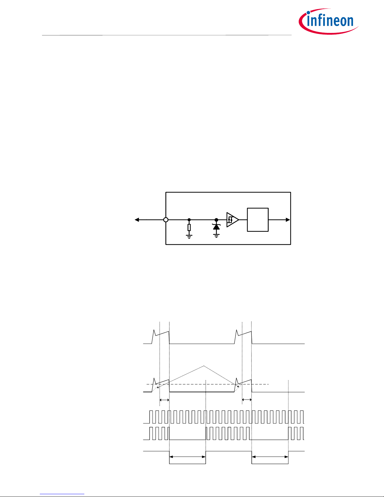
4.2 Over Current Protection
Over Current (OC) protection level is decided by ITRIP positive going threshold voltage (V
IT,TH+
) and current
sensing resistance. When the ITRIP voltage exceeds V
IT,TH+
, the module turns off all 3 IGBTs and the fault flag is
activated during fault-output duration time, typically 65µs.
Low Side IGBT
Collector Current
Sensing Voltage
of the shunt resistor
Fault Output Signal
OC Reference Voltage
RC circuit time
constant delay
OC
Typ. 65s Typ. 65s
t
ITRIP
LINx
LOx
t
ITRIP
OC
Page 7

AN2016-19 Application Note 7 <Revision 2.0>
<2018-02-06>
Key Parameters Setting
Control Integrated POwer System (CIPOS™)
3-Phase Interleaved PFC IPM (IFCMxxU65yz) Reference Board
Figure 5 Timing chart of OC protection
4.2.1 Current Sensing Resistor Selection
The value of the current sensing resistor can be calculated with the following equation.
OC
DROP DIODE FILTER,TH IT,
SH
I
VV
R
Where,
R
SH
: current sensing resistor value
V
IT,TH+
: ITRIP positive going threshold voltage, typ. 0.47V
V
FILTER, DIODEDROP
: voltage drop from RSH to ITRIP by ORing diode, typ. 0.62V (1N4148, IF=1mA, TJ=25°C)
I
OC
: over current level
A maximum value of the OC protection level should be set less than the maximum peak output current in the
datasheet absolute maximum ratings while taking into consideration the tolerance of the current sensing
resistor.
For example, the maximum peak output current of the IFCM20U65GD is 30A
peak
,
0.036Ω
30A
1.09V
30A
0.62V0.47V
R
SH(min)
So the recommended value of the current sensing resistor should be higher than 36mΩ for IFCM20U65GD.
In order to calculate the power rating of the current sensing resistor, the below items has to be taken into
account.
Maximum load current of the 3-phase interleaved PFC IPM (I
RMS
)
Current sensing resistor value at T
C
=25°C (RSH)
Power derating ratio of the current sensing resistor at T
SH
=100°C
Safety margin
And the power rating can be calculated with the equation below.
ratio Derating
marginSafety RI
P
SH
2
RMS
SH
For example, in case of IFCM20U65GD and RSH=36mΩ,
Max. load current of the 3-phase interleaved PFC IPM (I
RMS
) : 7A
RMS
Current sensing resistor value at Tc=25°C (R
SH
) : 0.036Ω
Power derating ratio of the current sensing resistor at T
SH
=100°C : 80%
Safety margin : 30%
.87W2
80%
130%0.0367A
P
2
SH
So the proper power rating of the current sensing resistor is recommended as more than 3W.
Page 8

AN2016-19 Application Note 8 <Revision 2.0>
<2018-02-06>
Key Parameters Setting
Control Integrated POwer System (CIPOS™)
3-Phase Interleaved PFC IPM (IFCMxxU65yz) Reference Board
Based on the equation, condition and calculation method above, some example values of minimum current
sensing resistance and required resistor power rating are introduced as shown in below Table 5 for CIPOS™ Mini
3-phase interleaved PFC IPM products. When choosing a proper current sensing resistance and its power rating,
an accurate OC protection level in the application setting should be taken into account for a correct over
current detection.
Table 5 Maximum peak current, shunt resistor value and required power rating
Product
Maximum Peak Current
Minimum Shunt
Resistance, RSH
Minimum Shunt Resistor
Power, PSH
IFCM20U65GD
30A
36mΩ
3.0W
IFCM30U65GD
40A
27mΩ
4.5W
4.2.2 Delay Time
The RC filter is necessary in the over current sensing circuit to prevent malfunction of OC protection caused by
noise. The RC time constant is determined by considering the noise duration and safety operation capability of
the IGBT.
When the sensing voltage on shunt resistor exceeds the ITRIP positive going threshold (V
IT,TH+
), this voltage is
applied to the ITRIP pin of CIPOS™ Mini via the RC filter. Table 6 shows the specification of the OC protection
reference level. The filter delay time (t
FILTER
) that the input voltage of ITRIP pin rises to the ITRIP positive
threshold voltage is caused by below equation (1), (2).
(1)
(2)
Where, V
IT,TH+
is the ITRIP pin input voltage, IC is the peak current, RSH is the shunt resistor value and τ is the RC
time constant. In addition there is a shutdown propagation delay of Itrip (t
ITRIP
). In addition there is a shutdown
propagation delay of Itrip (t
ITRIP
). Please refer to Table 7.
Table 6 Specification of OC protection reference level ‘V
IT,TH+
’
Item
Min.
Typ.
Max.
Unit
ITRIP positive going threshold V
IT,TH+
0.40
0.47
0.54
V
Table 7 Shut down propagation delay
Item
Condition
Min.
Typ.
Max.
Unit
Shut down
propagation delay
(t
ITRIP
)
IFCM20U65GD
I
out
=10A, from V
IT,TH+
to 10% I
out
-
1340
-
ns
IFCM30U65GD
I
out
=15A, from V
IT,TH+
to 10% I
out
-
1540
-
Therefore the total time from ITRIP positive going threshold (V
IT,TH+
) to the shut down of the IGBT becomes:
Shut down propagation delay is inversely proportional to the current range, therefore the t
ITRIP
is reduced at
higher current condition than condition of Table 7. The recommended total delay is less than the 5s of safety
operation. Thus, the RC time constant should be set in the range of 1~2µs. A recommended RC filter values are
1.8kΩ R11, 100Ω R9 & R12 & R14, 1nF C8 and 1nF C12 & C13 & C14.
Page 9

AN2016-19 Application Note 9 <Revision 2.0>
<2018-02-06>
Key Parameters Setting
Control Integrated POwer System (CIPOS™)
3-Phase Interleaved PFC IPM (IFCMxxU65yz) Reference Board
4.3 Temperature Monitor and Thermal Protection
In case of the CIPOS™ Mini 3-phase interleaved PFC IPM, a built-in thermistor (85kΩ at 25°C) is connected
between NTC and VSS pins. The typical application circuit looks like Figure 6 where the NTC pin is used for
thermistor temperature sensing and the VFO pin is used for fault flag. The voltage of the NTC pin decreases as
the thermistor temperature increases because the thermistor is an NTC (Negative Temperature Coefficient)
type and it is connected to the external pull-up resistor. Note that the voltage variation of the NTC pin, which is
generated by the thermistor temperature change, should be always inside the A/D converter input range of the
micro controller. In this reference board, the pull-up resistor is set to 3.6kΩ so that the NTC voltage becomes
2.95V and 1.95V respectively for 5V and 3.3V control voltage (VDD5V) when the thermistor temperature is 100°C,
as shown in Figure 7.
IFCMxxU65GD
Drive IC
VFO
R5=3.6kΩ
Thermistor
VFO
VDD5V
VSS
CIPOS
TM
Input to AD
Converter
Input to Fault
Detection
Micro
Controller
R3=3.6kΩ
NTC
VDD5V
Figure 6 Temperature monitor with built in thermistor and pull up resistor
0 10 20 30 40 50 60 70 80 90 100 110 120
0.0
0.5
1.0
1.5
2.0
2.5
3.0
3.5
4.0
4.5
5.0
OT set 100℃ : 1.95V at VDD5V=3.3V
OT set 100℃ : 2.95V at VDD5V=5V
VDD5V=5V
VDD5V=3.3V
V
NTC
[ V ]
o
Page 10

AN2016-19 Application Note 10 <Revision 2.0>
<2018-02-06>
Key Parameters Setting
Control Integrated POwer System (CIPOS™)
3-Phase Interleaved PFC IPM (IFCMxxU65yz) Reference Board
Figure 7 Voltage variation of the NTC pin along with the NTC thermistor temperature change
Page 11

AN2016-19 Application Note 11 <Revision 2.0>
<2018-02-06>
Boost PFC Circuit Setting
Control Integrated POwer System (CIPOS™)
3-Phase Interleaved PFC IPM (IFCMxxU65yz) Reference Board
5 Boost PFC Circuit Setting
5.1 Target Specification
Table 8 below shows a target specification example for the CIPOS™ Mini 3-phase interleaved PFC IPM reference
board.
Table 8 Design parameters for the proposed target specification
Design parameter
Parameter name
Value
Minimum input voltage
Vin_min
85VAC
Maximum input voltage
Vin_max
265VAC
Line frequency
fL
50Hz
Output voltage
Vout
390VDC
Minimum output voltage
Vout_min
250VDC
Output current
Iout
15.39A
Output power
Pout
6000W
Efficiency η >90% at full load
PFC switching frequency
fSW
40kHz
Maximum ambient temperature around PFC
T
Amax
70°C
5.2 Boost Inductor
The maximum input RMS current, I
in_RMS
, is needed to obtain 6000W output power P
out
with 85V minimum AC
input voltage V
in_min
. The equation below shows the calculation example for a maximum input RMS current.
A
V
43.78
%9058
6000W
V
P
I
in_min
out
in_RMS
The sinusoidal peak value of AC current, I
in_pk
, is calculated as below.
AA 92.11043.782I2I
in_RMSin_pk
The IHF represents a high frequency ripple current peak to peak on the boost inductor. It is related to maximum
input power and minimum input voltage as below.
in_min
in_max_PH
HF
V
P
2I k
phaseofNo __
P
P
out_max
in_max_PH
The “k” is a ratio of inductor ripple current based on the inductor average current. It must be kept reasonably
small, and it is usually optimized in the range of 15% to 25% for cost effective design based on the current
magnetic component status. For example, if k=22%, then,
Ak 13.8
85V
1
390%
6000W
2%22
V
P
2I
in_min
in_max_PH
HF
Page 12

AN2016-19 Application Note 12 <Revision 2.0>
<2018-02-06>
Boost PFC Circuit Setting
Control Integrated POwer System (CIPOS™)
3-Phase Interleaved PFC IPM (IFCMxxU65yz) Reference Board
The peak current passing through the inductor is,
A
phaseofNo
97.36
3
110.92A
__
I
I
in_peak
in_peak_PH
AA 04.41
2
8.13A
97.36
2
I
II
HF
in_peak_PHL_pk
The on-duty of the transistor switch in a boost converter operating under CCM at minimum AC input RMS
voltage is,
692.0
390V
85V2
1
V
V2
1D
out
in_min
on
The boost choke inductor value is,
SWHF
in_minon
SWHF
outonon
boost
I
2VD
I
V)D-(1D
L
ff
Calculating the equation above with the value of Don=0.692 will generate the L
boost
value as below.
H
kHzA
V
f
256
408.13
258692.0
I
2VD
L
SWHF
in_minon
boost
The core material of the boost inductor can be either magnetic powder or ferrite. For further detailed design of
boost inductor, please refer to the PFC controller related document or appropriate application note.
5.3 Output Capacitor
An output bulk capacitor has to meet the requirement for output double line frequency ripple limit as the
equation below. The Vout_ripple is normally defined as lower than 10% of Vout. For example, 3% of 390VDC
Vout is around 12V of Vout_ripple. The equation below shows a calculation example of minimum output
capacitance.
F
VHzVf
4082
12502
15.39A
2
I
C
out_rippleL
OUT
OUT
The output capacitor of PFC circuit also has to supply enough energy to the next stage during hold-up time. The
20ms hold-up time is based on the line frequency of 50Hz. The output capacitor value should be higher than the
result of the equation below for hold-up time requirement.
F
VV
msW
VV
tP
outout
2679
250390
2060002
2
C
222
min_
2
holdupOUT
OUT
Comparing with two output capacitor calculation values above, the 4082µF capacitor can be chosen, but a max.
20% capacitance tolerance should be considered. So around 4900µF capacitor is finally recommended for the
output capacitor.
Page 13

AN2016-19 Application Note 13 <Revision 2.0>
<2018-02-06>
Part List
Control Integrated POwer System (CIPOS™)
3-Phase Interleaved PFC IPM (IFCMxxU65yz) Reference Board
6 Part List
Table 9 Part list (Only for reference. Supplier can be changed.)
Symbol
Components
Description
Supplier
R1 ~ R3
100Ω, 5%, 2012
Filter resistors for LIN(X), LIN(Y) and LIN(Z) signal input
Walsin
R4
3.6kΩ, 1%, 2012
Pull-up resistor to VDD5V for NTC supply voltage
Walsin
R5
1kΩ, 5%, 2012
Filter resistor for VFO signal output
Walsin
R6
3.6kΩ, 1%, 2012
Pull-up resistor to VDD5V for VFO supply voltage
Walsin
R7
1kΩ, 5%, 2012
Filter resistor for NTC signal output
Walsin
R8, R10,
R13, R15,
R17, R18
100Ω, 1%, 2012
Series resistors for current sensing signal interface
Walsin
R9, R12, R14
100Ω, 1%, 2012
Filter resistors for current sensing signal input
Walsin
R11
1.8kΩ, 1%, 2012
Filter resistor for current sensing signal input
Walsin
R16
3kΩ, 1%, 2012
Pull-down resistor for current sensing signal input
Walsin
RS1 ~ RS3
Refer to 4.2.1
Shunt resistors for current sensing
Vishay
C1 ~ C3
1nF, 50V, X7R, 10%
Filter capacitors for LIN(X), LIN(Y) and LIN(Z) signal
input
Walsin
C4
1nF, 50V, X7R, 10%
Filter capacitor for VFO signal output
Walsin
CP1
100uF, 35V
Bulk capacitor for VDD5V supply voltage
Samyoung
C5
100nF, 50V, X7R,
10%
Bypass capacitor for VDD5V supply voltage
Walsin
C6
1nF, 50V, X7R, 10%
Bypass capacitor for VFO supply voltage
Walsin
CP2
220uF, 35V
Bulk capacitor for VDD15V supply voltage
Samyoung
C7
100nF, 50V, X7R,
10%
Bypass capacitor for VDD15V supply voltage
Walsin
C8
1nF, 50V, X7R, 10%
Filter capacitor for current sensing signal input
Walsin
C9
1nF, 50V, X7R, 10%
Filter capacitor for NTC signal output
Walsin
C10
1nF, 50V, X7R, 10%
Bypass capacitor for NTC supply voltage
Walsin
C11
0.1uF, 630V
Snubber capacitor to reduce switching noise
Pilkor
C12 ~ C14
1nF, 50V, X7R, 10%
Filter capacitor for current sensing signal input
Walsin
D1 ~ D3
LL4148
ORing diodes for current sensing signal input
STMicro
D4 ~ D6
RS1K
Freewheeling diodes for boost PFC
Vishay
CN1
SMW250-11P
11-pin connector for signal and power supply
Yeonho
CN2
SMW250-6P
6-pin connector for current sensing signal
Yeonho
CN3
SMW250-3P
3-pin connector for current sensing signal
Yeonho
J1 ~ J6
Fasten Tap
Power terminals
KET
U1
IFCM20U65GD
CIPOS™ Mini 3-phase interleaved PFC IPM
Infineon
Technologies
Page 14

AN2016-19 Application Note 14 <Revision 2.0>
<2018-02-06>
PCB Design Guide
Control Integrated POwer System (CIPOS™)
3-Phase Interleaved PFC IPM (IFCMxxU65yz) Reference Board
7 PCB Design Guide
In general, there are several issues to be considered when designing a switching power supply application.
Low stray inductive connection
Isolation distance
Component placement
This chapter will explain about the items above and come up with the solutions for the better layout design.
7.1 Layout of Reference Board
Top view
Bottom view
Figure 8 Layout of reference board for 3-shunt resistors
Page 15

AN2016-19 Application Note 15 <Revision 2.0>
<2018-02-06>
PCB Design Guide
Control Integrated POwer System (CIPOS™)
3-Phase Interleaved PFC IPM (IFCMxxU65yz) Reference Board
1. The connection between emitters of CIPOS™ Mini 3-phase interleaved PFC IPM (NX, NY and NZ) and current
sensing resistors should be as short and as wide as possible.
2. It is recommended that the ground pin of the micro-controller should be directly connected to the VSS pin.
Signal ground and power ground should be as short as possible and connected at only one point via the VDD
capacitor (C7).
3. All of the bypass capacitors should be placed as close to the pins of CIPOS™ Mini 3-phase interleaved PFC IPM
as possible.
4. The capacitor (C8) for voltage sensing of the current sensing resistor should be placed as close to ITRIP and
VSS pins as possible.
5. In order to accurately detect the voltage of the current sensing resistor, both sensing and ground patterns
should be connected at the pins of the current sensing resistor and should not be overlapped with any
patterns for the load current, as shown in Figure 8.
6. The snubber capacitor (C11) should be placed as close to the power terminals as possible.
7. The PCB routings for power pins such as P, X, NX, Y, NY, Z and NZ should be placed on both top and bottom
layers with vias to allow high current flowing. They have to keep the minimum isolation distance among the
power patterns. The distance should be at least over than 2.54mm.
8. Note that there are milling profiles in gray lines on the board to keep the isolation distance.
9. All components except the CIPOS™ Mini 3-phase interleaved PFC IPM are placed on the top layer.
Page 16

AN2016-19 Application Note 16 <Revision 2.0>
<2018-02-06>
Peripheral Components Connection
Control Integrated POwer System (CIPOS™)
3-Phase Interleaved PFC IPM (IFCMxxU65yz) Reference Board
8 Peripheral Components Connection
This reference board is composed of IFCM20U65GD, minimum peripheral components and three current
sensing resistors. So, in order to operate the reference board by 3-phase interleaved PFC topology, users need
to set up additional external system and components such as bridge rectifier, boost inductor, main DC link
capacitor, power supply, PFC control system, and resistive load.
Figure 9 is example of system setup for evaluation of the 3-phase interleaved PFC IPM reference board.
MCU /
PFC Controller
LIN(A), LIN(B)
VFO, NTC
Vctr
Vctr, VDD,
GND
Current Sensing Signal(CS1, CS2, CS3, GND)
X
Z
N2 P
Main DC Link
(VDC)Capacitor
SMPS
P
Boost Inductor
P
Bridge
Rectifier
AC INPUT
Y
Inductor
N2
N1
Resistive Load
Figure 9 System setup with reference board
Page 17

AN2016-19 Application Note 17 <Revision 2.0>
<2018-02-06>
Evaluation Example of Reference Board
Control Integrated POwer System (CIPOS™)
3-Phase Interleaved PFC IPM (IFCMxxU65yz) Reference Board
9 Evaluation Example of Reference Board
9.1 Evaluation Results
Table 1 Evaluation Setup [DUT: IFCM20U65GD]
Design parameter
Parameter name
Value
Input voltage
Vin
220 [Vac]
Line frequency
fL
60 [Hz]
Output voltage
V
out
400 [VDC]
Output power
P
out
5000 [W]
Main boost inductance
L
boost
100 [μH]
PFC switching frequency
fSW
40 [kHz]
Cooling Method
-
Force cooling by fan
Load - Resistive load
Figure 10 Operating waveform (CH1: Input voltage, CH2: Input current, CH3: Output voltage, CH4:
Output current) and Case temperature (TC)
Input Conditions
Output Conditions
Power
Factor
Efficiency
[%]
Case
Temperature
[°C]
Voltage [Vac] /
Frequency [Hz]
Current
[Arms]
Power
[kW]
Voltage
[Vrms]
Current
[Arms]
Power
[kW]
220/60
23.45
5.16
400
12.43
4.97
0.99
96.3
48.0
VIN [100V/div]
Time [5ms/div.]
V
out
[100V/div]
IIN [10A/div]
Io [5A/div]
Page 18

AN2016-19 Application Note 18 <Revision 2.0>
<2018-02-06>
Reference
Control Integrated POwer System (CIPOS™)
3-Phase Interleaved PFC IPM (IFCMxxU65yz) Reference Board
10 Reference
[1] Infineon Power Semitech: CIPOS™ IFCM20U65GD; Datasheet Ver1.0; Infineon Power Semitech, 2016
[2] Infineon Power Semitech: Design Guide for Boost Type CCM PFC with ICE2PCSxx, 2008
Page 19

Other Trademarks
All referenced product or service names and trademarks are the property of their respective owners.
Edition <2018-02-06>
AN2016-19 Application Note
Published by
Infineon Technologies AG
81726 Munich, Germany
© 2018 Infineon Technologies AG.
All Rights Reserved.
Do you have a question about this
document?
Email: erratum@infineon.com
Document reference
IMPORTANT NOTICE
The information contained in this application note
is given as a hint for the implementation of the
product only and shall in no event be regarded as a
description or warranty of a certain functionality,
condition or quality of the product. Before
implementation of the product, the recipient of this
application note must verify any function and other
technical information given herein in the real
application. Infineon Technologies hereby
disclaims any and all warranties and liabilities of
any kind (including without limitation warranties of
non-infringement of intellectual property rights of
any third party) with respect to any and all
information given in this application note.
The data contained in this document is exclusively
intended for technically trained staff. It is the
responsibility of customer’s technical departments
to evaluate the suitability of the product for the
intended application and the completeness of the
product information given in this document with
respect to such application.
For further information on the product, technology,
delivery terms and conditions and prices please
contact your nearest Infineon Technologies office
(www.infineon.com).
Please note that this product is not qualified
according to the AEC Q100 or AEC Q101 documents
of the Automotive Electronics Council.
WARNINGS
Due to technical requirements products may
contain dangerous substances. For information on
the types in question please contact your nearest
Infineon Technologies office.
Except as otherwise explicitly approved by Infineon
Technologies in a written document signed by
authorized representatives of Infineon
Technologies, Infineon Technologies’ products may
not be used in any applications where a failure of
the product or any consequences of the use thereof
can reasonably be expected to result in personal
injury.
 Loading...