


Data Sheet, V 1.0, May 2003
C868
8-Bit Single-Chip Microcontroller
Microcontrollers
Never stop thinking.

Edition 2003-05
Published by Infineon Technologies AG,
St.-Martin-Strasse 53,
D-81541 München, Germany
© Infineon Technologies AG 2003.
All Rights Reserved.
Attention ple ase!
The information herein is given to describe certain components and shall not be considered as warranted
characteristics.
Terms of delivery and rights to technical change reserved.
We hereby disclaim any and all warranties, including but not limited to warranties of non-infringement, regarding
circuits, descriptions and charts stated herein.
Infineon Technologies is an approved CECC manufacturer.
Information
For further information on technology, delivery terms and conditions and prices please contact your nearest
Infineon Technologies Office in Germany or our Infineon Technologies Representatives worldwide (see address
list).
Warnings
Due to technical requirements components may contain dangerous substances. For information on the types in
question please contact your nearest Infineon Technologies Office.
Infineon Technologies Components may only be used in life-support devices or systems with the express written
approval of Infineon T echnologies, if a failure of such components can reasonably be expected to cause the failure
of that life-support device or system, or to affect the safety or effectiveness of that device or system. Life support
devices or systems are intended to be implanted in the human body, or to support and/or maintain and sustain
and/or protect human life. If they fail, it is reasonable to assume that the health of the user or other persons may
be endangered.

Data Sheet, V 1.0, May 2003
C868
8-Bit Single-Chip Microcontroller
Microcontrollers
Never stop thinking.

C868
Revision History: 2003-05 V 1.0
Previous Version: Page Subjects (major changes since last revision)
Current data updated
Description of I2C included
We Listen to Your Comments
Any information within this document that you feel is wrong, unclear or missing at all?
Your feedback will help us to continuously improve the quality of this document.
Please send your proposal (including a reference to this document) to:
mcdocu.comments@infineon.com
C8688-Bit Single-Chip Microcontroller
C800 Family
C868
Advance Information
• C800 core :
–Fully compatible to standard 8051 microcontroller
–Superset of the 8051 architecture with 8 datapointers
• 40 MHz internal CPU clock
–external clock of 6.67 - 10.67 MHz at 50% duty cycle
–300 ns instruction cycle ti me (@37.5 MHz CPU cloc k)
• 8 Kbyte on-chip Program ROM for C868-1R and 8 KByte on-chip Program RAM for
C868-1S
• In-system programming support for programming the XRAM(C868-1R) or XRAM/
Program RAM(C868-1S)
–This feature is realized through 4KB Boot ROM
• 256 byte on-chip RAM
• 256 byte on-chip XRAM
(further features are on the next page)
RAM
256 × 8
XRAM
256 × 8
ROM/RAM
8K × 8
Boot ROM
4K x 8
Timer 0
Timer 1
CPU
8 datapointers
Watchdog Timer
8-bit
UART
Timer 2
16-bit
Capture/
Compare
Unit
16-bit Compare
Unit
8-Bit ADC
Port 1
Port 3
I/O
5-bit
Input
3-bit
I/O
8-bit
Analog/
Digital
Input
Figure 1 C868 Functional Units
Data Sheet 5 V 1.0, 2003-05

C868
• One 8-bit and one 5 bits general purpose push-pull I/O ports
– Enhanced sink current o f 10 mA on Port 1/3 (total max current of 43 mA @ 100
• Three 16-bit timers/counters
–Timer 0 / 1 (C501 compatible)
–Timer 2 (up/down counter feature)
–Timer 1 or 2 can be used for serial baudrate generator
• Capture/compare unit for PWM signal generation
–3-channel, 16-bit capture/compare unit
–1-channel, 16-bit compare unit
• Full duplex serial interface (UART)
• 5 channel 8-bit A/D Converter
– Start of conversion can be synchronized to capture/compare timer 12/13.
• 13 interrupt vectors with four priority levels
• Programmable 16-bit Watchdog Timer
• Brown out detection
• Power Saving Modes
–Slow-down mode
–Idle mode (can be combined with slow-down mode)
–Power-down mode with wake up capability through INT0
or RxD pins.
• Single power supply of 3.3V, internal voltage regulator for core voltage of 2.5V.
• P-DSO-28-1, P-TSSOP-38-1 packages
• Temperature ranges:
SAF-C868-1RR BA, SAF-C868-1SR BA, SAF-C868-1RG BA, SAF-C868-1SG BA,
SAF-C868A-1RR BA, SAF-C868A-1SR BA, SAF-C868A-1RG BA, SAF-C868A-1SG
BA, SAF-C868P-1SR BA, SAF-C868P-1SG BA T
= – 40 to 85 oC
A
SAK-C868-1RR BA, SAK-C868-1SR BA, SAK-C868-1RG BA, SAK-C868-1SG BA,
SAK-C868A-1RR BA, SAK-C868A-1SR BA, SAK-C868A-1RG BA, SAK-C868A-1SG
BA, SAK-C868P-1SR BA, SAK-C868P-1SG BA T
= – 40 to 125 oC
A
o
C)
Data Sheet 6 V 1.0, 2003-05
C868
V
DDPVSSP
V
AREF
V
AGND
Port 1
5-bit Digital I/O
3-bit Digial Input
Port 3
RESET
ALE/BSL
CTRAP
TxD
RxD
C868
8-bit Digital I/O
5 ADC channels
4 External
Interrupts
V
V
DDC
SSC
Figure 2 Logic Symbol
Data Sheet 7 V 1.0, 2003-05
C868
P1.4/RxD
P1.3/INT3
P1.1/EXF2
P1.0/TxD
P1.5/CCPOS0/T2/INT0
P1.6/CCPOS1/T2EX/INT1
P1.7/CCPOS2/INT2/AN2
V
/AN0
/AN1
V
AGND
V
P1.2
NC
NC
NC
DDP
V
SSP
AREF
AN3
AN4
NC
NC
1
2
3
4
5
6
7
8
9
10
11
12
13
14
15
16
17
18
19
C868
RESET
38
37
P3.7/CC60
36
P3.6/COUT60
35
NC
34
ALE/BSL
33
P3.1/CTRAP
32
P3.0/COUT63
31
P3.4/COUT61
30
XTAL2
29
XTAL1
28
V
27
V
26
P3.3/CC62
25
P3.2/COUT62
24
P3.5/CC61
23
NC
22
NC
21
NC
20
NC
DDC
SSC
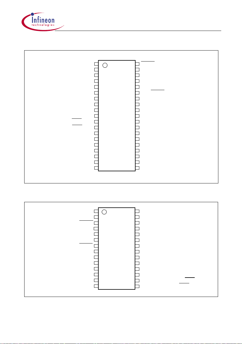
Figure 3 C868 Pin Configuration P-TSSOP-38 Package (top view)
P3.4/COUT61
P3.0/COUT63
P3.1/CTRAP
ALE/BSL
P3.6/COUT60
P3.7/CC60
RESET
P1.4/RxD
P1.3/INT3
P1.2
P1.1/EXF2
P1.0/TxD
V
DDP
V
SSP
1
2
3
4
5
6
7
8
9
10
11
12
13
14
C868
XTAL2
28
27
XTAL1
26
V
DDC
25
V
SSC
P3.3/CC62
24
P3.2/COUT62
23
P3.5/CC61
22
21
AN4
20
AN3
19
V
AREF
18
V
AGND
17
P1.7/CCPOS2/INT2/AN2
16
P1.6/CCPOS1/T2EX/INT1/AN1
15
P1.5/CCPOS0/T2/INT0
/AN0
Figure 4 C868 Pin Configuration P-DSO-28 Package (top view)
Data Sheet 8 V 1.0, 2003-05
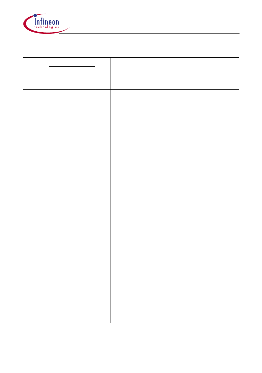
Table 1 Pin Definitions and Functions
Symbol Pin Numbers I/O*) Function
P1.0–
P1.4
P1.5P1.7
PDSO28
12-8
15-17
PTSSOP38
6,4-1
11-13
I/OIPort 1
is a combination of 5 bits of pus h-pull bi directiona l I/
O ports and 3 bits of input ports.
As alternate digital functions, port 1 contains the
interrupt 3, timer 2 overflow flag, rece ive data input
and transmit data output of serial interface. The
alternate functions are assigned to the pins of port
1 as follows:
12
11
10
9
8
6
4
3
2
1
P1.0/TxD Transmit data of serial interface
P1.1/EXF2 Timer 2 overflow flag
P1.2
P1.3/INT3 Interrupt 3
P1.4/RxD Receive data of serial interface, Use as
wakeup source from powerdown if bit WS of
PMCON0 is set.
C868
The input ports are a ls o i nte rrupt po rts , i npu t to th e
timer2, CCU6 modules and ADC:
15 11 I P1.5/Input to Counter 2/External Interrupt 0 Input/
Analog Input Channel 0
External interrupt input or Hall input signal , counte r
2 input or input channel 0 to the ADC unit. Use as
wakeup source from powerdown if bit WS of
PMCON0 is cleared.
16 12 I P1.6/Timer 2 Trigger/External Interrupt 1 Input/
Analog Input Channel 1
External interrupt input or Hall input signal, input
channel 1 to the ADC unit, trigger to Timer 2.
17 13 I P1.7/External Interrupt 2 Input/
Analog Input Channel 2
External interrupt input or Hall input signal and inpu t
channel 2 to the ADC unit.
*)I=Input
O=Output
Data Sheet 9 V 1.0, 2003-05
Table 1 Pin Definitions and Functions
Symbol Pin Numbers I/O*) Function
P3.0–
P3.7
PDSO28
2,3,23,
24,1,
22,5,6
PTSSOP38
32,33,25,
26,31,24,
36,37
I/O Port 3
is an 8-bit push-pull bidirec tio nal I/O po rt. Thi s po rt
also serves as alternate functions for the CCU6
functions. The functions are assigned to the pins of
port 3 as follows :
C868
V
AREF
V
AGND
2
3
23
24
1
22
5
6
19 15 – Reference voltage for the A/D converter.
18 14 – Reference ground for the A/D converter.
32
33
25
26
31
24
36
37
P3.0/COUT63 16 bit compare channe l outp ut
P3.1/CTRAP CCU trap input
P3.2/COUT62 Output of capture/compare ch 2
P3.3/CC62 Input/output of capture/compare ch 2
P3.4/COUT61 Output of capture/compare ch 1
P3.5/CC61 I nput/outpu t of capture/compare ch 1
P3.6/COUT60 Output of capture/compare ch 0
P3.7/CC60 Input/output of capture/compare ch 0
AN4 21 17 I Analog Input Channel 4
is input channel 4 to the ADC unit.
AN3 20 16 I Analog Input Channel 3
is input channel 3 to the ADC unit.
RESET
738 IRESET
A low level on this pin for two machine cycle while
the oscillator is running resets the device.
ALE/BSL 4 34 I/O Address Latch Enable/Bootstrap Mode
A low level on th is pin during res et allows the d evice
to go into the bootstrap mode. After reset, this pin
will output the address latch enable signal. The
ALE can be disabled by bit EALE in SFR
SYSCON0.
V
V
SSP
DDP
14 10 – IO Ground (0V)
13 9 – IO Power Supply (+3.3V)
*)I=Input
O=Output
Data Sheet 10 V 1.0, 2003-05
Table 1 Pin Definitions and Functions
Symbol Pin Numbers I/O*) Function
V
V
SSC
DDC
PDSO28
25 27 – Core Ground (0V)
26 28 O Core Internal Reference (+2.5V)
PTSSOP38
Connect 2*68 - 470nF ceramic capacitor across
this pin and core ground.
NC – 5,7,8,18,
– Not connected
19,20,21,
22,23,35
XTAL1 27 29 I XTAL1
Output of the inverting oscillator amplifier.
XTAL2 28 30 O XTAL2
Input to the inverting os cillator amplifier an d input to
the internal clock generation circuits.
To drive the device from an external clock sourc e,
XTAL2 should be driven, while XTAL1 is left
unconnected.
*)I=Input
O=Output
C868
Data Sheet 11 V 1.0, 2003-05
V
DDC
V
SSC
XTAL1
XTAL2
C868
OSC
PLL
XRAM
256 x 8
RAM
256 x 8
ROM/
RAM
8k x 8
C868
Boot/
Self
Test
ROM
4k x 8
RESET
4 external
interrupts
V
AREF
V
AGND
5-Bit
Analog In
CPU
8 datapointers
Programmable
Watchdog Timer
Timer 0
Timer 1
Timer 2
UART
Capture/Compare
Unit
Interrupt Unit
A/D Converter
8-Bit
Port 1
Port 3
Port 1
5-bit
digital
I/O
and
3-bit
digital
input
Port 3
8-bit
digital
I/O
V
DDP
V
SSP
Figure 5 Block Diagram of the C868
Data Sheet 12 V 1.0, 2003-05
C868
CPU
The C868 is efficient both as a controller and as an arithmeti c processor. It has extens ive
facilities for bi nary and BCD ar ithmetic and e xcels in i ts bit-handli ng capabili ties. Efficie nt
use of program memory results from an instruction set consisting of 44% one-byte, 41%
two-byte, and 15% three-byte instructions. With a 10.67 MHz external crystal (giving a
40MHz CPU clock), 58% of the instructions execute in 300 ns.
PSW
Program Status Word Register [Reset value: 00
D7
H
CY AC F0 RS1 RS0 OV F1 P
rwh rwh rw rw rw rwh rw rwh
D6
H
D5
H
D4
H
D3
H
D2
H
D1
H
Field Bits Typ Description
P 0rwhParity Flag
Set/cleared by hardware after each instruction to
indicate an odd/even number of "one" bits in the
accumulator, i.e. even parity.
F1 1rwGeneral Purpose Flag
OV 2rwhOverflow Flag
Used by arithmetic in structions.
RS0
RS1
3
4
rw Register Bank select control bits
These bits are used to select one of the four register
banks.
Table 2 :
RS1 RS0 Function
0 0 Bank 0 selected, data address 00H-07
0 1 Bank 1 selected, data address 08H-0F
1 0 Bank 2 selected, data address 10H-17
1 1 Bank 3 selected, data address 18H-1F
D0
H
H
H
H
H
H
]
F0 5rwGeneral Purpose Flag
AC 6rwhAuxiliary Carry Flag
Used by instruction s which exec ute BCD operations .
CY 7rwhCarry Flag
Used by arithmetic in structions.
Data Sheet 13 V 1.0, 2003-05
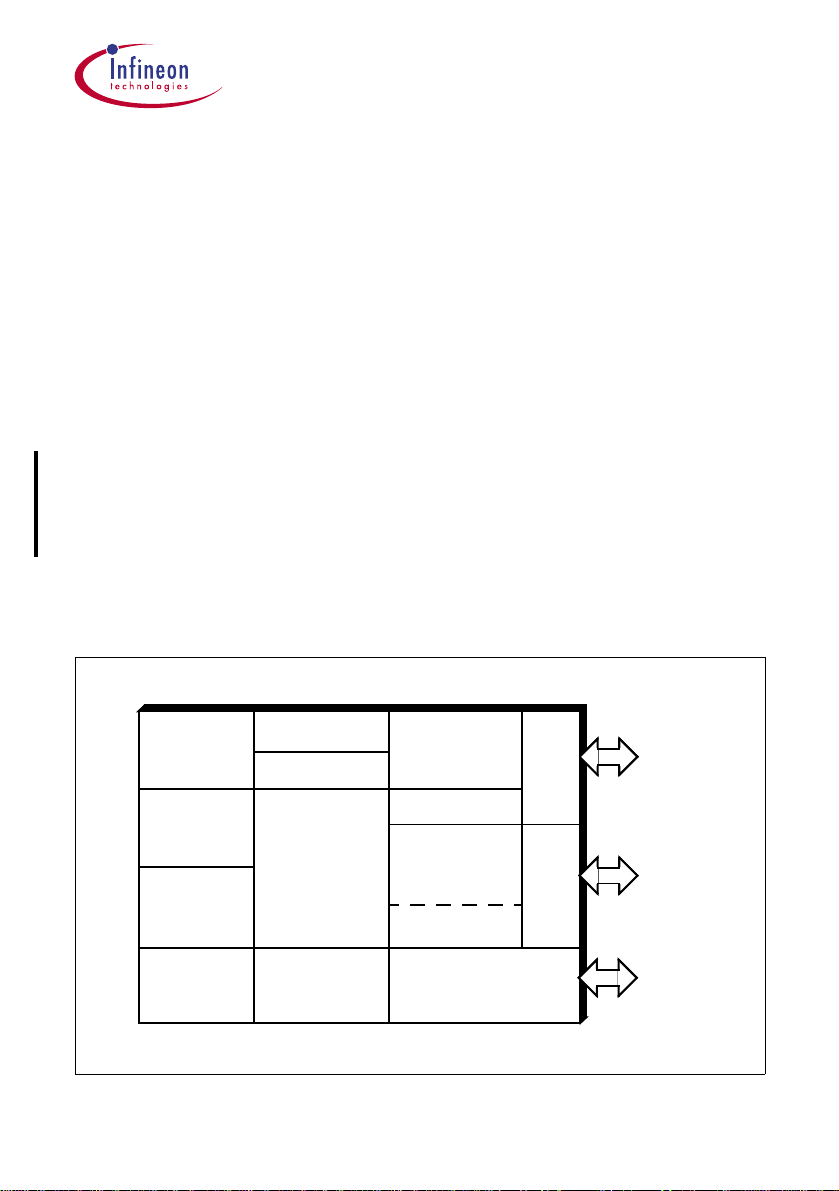
Memory Organization
The C868 CPU manipulates operands in the following five address spaces:
– up to 8 Kbyte of RAM internal program memory : 8K ROM for C868-1R
: 8K RAM for C868-1S
– 4 Kbyte of internal Self test and Boot ROM
– 256 bytes of internal data memory
– 256 bytes of internal XRAM data memory
– 128 byte special function register area
Figure 0-1 illustrates the memory address spaces of the C868.
FFFF
FF00
H
H
indirect
addr.
Internal
RAM
Function
Internal
RAM
Internal
Self Test
and Boot
ROM
(4 KByte)
Internal
1FFF
0000
Internal
XRAM
H
H
direct
addr.
Special
Regs.
7F
00
H
H
C868
FF
H
80
H
"Code Space"
"Data Space"
"Internal Data Space"
Figure 0-1 C868 Memory Map
Data Sheet 14 V 1.0, 2003-05
The various chip modes supported are shown in Figure 6.
Normal
Mode
C868
Bootstrap
Mode
Normal
XRAM
Mode
Bootstrap
XRAM
Hardware
Software
Mode
Figure 6 Entry and exit of Chip Modes
A valid hardware reset would, of course, override any of the above entry or exit
procedures.
Table 0-1 Hardware and Software Selection of Chipmodes
Operating Mode
Hardware Selection Software Selection
(Chipmode)
Normal Mode ALE/BSL pin = high
RESET
rising edge
ALE/BSL = don’t care;
setting bits BSLEN, SWAP = 0,0;
execute unlocking sequence
Normal XRAM Mode Not possible setting bits BSLEN,SWAP = 0,1;
execute unlocking sequence
Bootstrap XRAM Mode Not possible setting bits BSLEN,SWAP = 1,1;
execute unlocking sequence
Bootstrap Mode ALE/BSL pin = low
RESET rising edge
ALE/BSL = don’t care;
setting bits BSLEN, SWAP = 1,0;
execute unlocking sequence
Data Sheet 15 V 1.0, 2003-05
Table 3 Normal Memory Configuration
C868
Chip
Memory Space Memory Boundary
Mode
Normal Code Space ROM/RAM: 0000
Internal Data Space XRAM: FF00H to FFFF
to 1FFF
H
H
Bootstrap Code Space Boot ROM: 0000H to 0FFF
Internal Data Space XRAM: FF00H to FFFF
H
ROM/RAM: 0000H to 1FFF
Normal
XRAM
Bootstrap
XRAM
Code Space XRAM: FF00H to FFFF
H
Data Space ROM/RAM: 0000H to 1FFF
Code Space Boot ROM: 0000H to 0FFF
XRAM: FF00H to FFFF
H
Data Space ROM/RAM: 0000H to 1FFF
H
H
H
H
H
H
Data Sheet 16 V 1.0, 2003-05

C868
Bootstrap loader
The C868, includes a bootstrap mode, which is activated by setting the ALE/BSL pin at
logic low with a pul ld ow n and Tx D p in at logic high with a pu llup at the rising e dg e o f th e
. Or it can be entered by software, that is by setting BSLEN bit and resetting
RESET
SWAP bit in SFR SYSCON1 accompany by an unlock sequence.
In the bootstrap mode , software routi nes of the b ootstrap load er located in th e boot ROM
will be executed. Its pur pos e i s to allow the easy and quick programmin g of the int ernal
SRAM (0000
the MCU is in-circuit. It also provides a way to program SRAM or XRAM through
bootstrapping from an external SPI or I2C EEPROM.
The first action of the bootstrap lo ader is to detect the presence of EEPROM and its type,
SPI or I2C, and check the first byte of the serial EEPROM. If the first byte is 0A5
MCU would enter Phase A to download from the EEPROM. Otherwise, it will enter
Phase B to establish a serial communication with the connected host. Bootstrapping
from the serial EEPROM can also be done in phase B if it is invoked by the host.
Phase B consists of two functional parts that represent two phases:
• Phase I: Establish a serial connection and automatically synchronize to the transfer
speed (baud rate) of the serial communication partner (host).
• Phase II: Perform the serial communication with the host. The host controls the
communication by sending special header information, which select one of the
working modes. These modes are:
to 1FFFH) or XRAM (FF00H to FFFFH) via serial interface (UART) while
H
H
, the
Table 4 Serial Communication Modes of Phase B
Modes Description
0 Transfer a customer program from the host to the SRAM (0000
) or XRAM (FF00H -FFFFH). Then return to the beginning of
1FFF
H
to
H
phase II and wait for the next command from the host.
1 Execute a customer program in the XRAM at start address FF00
2 Execute a customer program in the SRAM at start address 0000
.
H
.
H
3 Transfer a customer program from the SPI EEPROM to the SRAM
(0000H to 1FFFH) or XRAM (FF00H -FFFFH). Then return to the
beginning of phase II and wait for the next command from the host.
4 Transfer a customer program from the I2C EEPROM to the SRAM
(0000
to 1FFFH) or XRAM (FF00H -FFFFH). Then return to the
H
beginning of phase II and wait for the next command from the host.
5-9 reserved
The phases of the bootstrap loader are illustrated in Figure 7.
Data Sheet 17 V 1.0, 2003-05
Phase A
Bootstrap from
serial
EEPROM
EEPROM (first byte)
Yes
Start
Read serial
byte=A5H? No
Init serial interface 0
and synchronize to
the host baud rate
Phase B
Receive header
block from host
C868
Phase B, Phase I
Phase B, Phase II
Activate Mode 4
Load program from
I2C serial EEPROM
to SRAM/XRAM
Activate Mode 3
Activate mode 0
Load custom code
to SRAM/XRAM
Activate Mode 1
Execute custom
program in XRAM
Select working
mode
Activate Mode 2
Execute custom
program in SRAM
Load program from SPI serial
EEPROM to SRAM/XRAM
Figure 7 The phases of the Bootstrap Loader
The serial communication is activated in phase B. Using a full duplex serial cable
(RS232), the MCU must be connected to the serial port of the host computer as shown
in Figure 8.
Serial Cable
PC
full duplex, RS232
C868
Host Computer
Serial Interface
(asynchronous, 8N1)
Serial Interface,
UART Mode 1
(asynchronous, 8N1)
Figure 8 Bootstrap Loader Interface to the PC
Data Sheet 18 V 1.0, 2003-05
C868
VCC VCC
P1.3
P1.1
P1.2
240R
1
/CS
6
SCK
5
SI
2
SO
/HOLD
/WP
VCC
GN
7
3
8
4
D
1
A0
6
A1
5
A2
2
GN
D
VCC
WP
SCL
SDA
7
3
8
4
3K3
P1.1
P1.2
a) SPI EEPRO M connection
b) I2C EEPROM connection
Figure 9 EEPROM connections for a) SPI and b) I2C
Data Sheet 19 V 1.0, 2003-05
C868
Reset and Brownout
The reset input is an active low input. An internal Schmitt trigger is used at the input for
noise rejection. The RESET
only exit from reset condition after the PLL lock had been detected.
During RESET
at transition from low to high, C868 will go into normal mode if ALE/BSL
is high and bootstrap loading mode if ALE/BSL is low. A pullup to V
ground is recommended for pin ALE/BSL. TXD should have a pu llup to V
not be stimulated externally during reset, as a logic low at this pin will cause the chip to
go into test mode if ALE/BSL is low.
Figure 10 shows the possible reset circuits, note that the RESET
internal pullup resistance.
pin must be held low fo r at l east tbd usec . Bu t the CPU will
or pulldown to
DDP
and should
DDP
pin does not have an
a)
V
DDP
C868 BA
RESET
b) c)
C868 BA
&
RESET
V
DDP
C868 BA
RESET
Figure 10 Reset Circuitries
An on-chip analog circuit detects brownout, if the core voltage V
threshold voltage V
THRESHOLD
active for tbd usec then the device will reset. When V
V
THRESHOLD
while RESET is high, the reset is released once PLL is locked for 4096
momentarily while RESET pin is high. If this detect ion is
recovers by exceeding
DDC
dips below the
DDC
clocks. Bit BO in the PMCON0 register is set when brownout detected if brownout
detection was enabled, this bit is cleared by hardware reset RESET and software. All
ports are tristated during brownout.
The V
THRESHOLD
has a nominal value of 1.47V, a minimum value of 1.1V and a
maximum value of 1.8V.
Data Sheet 20 V 1.0, 2003-05
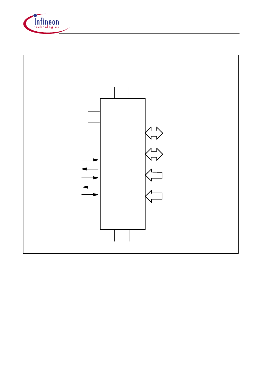
C868
Clock system
The C868 clock system cons ist of the on-chip oscillat or, PLL and m ultipl exer sta ge. The
programmable Slow Down Divider (SDD) divides the PLL output clock frequency by a
factor of 1...32 which is specified via CMCON.REL. The system clock is switched from
the PLL output to the output from the SDD when slowdown mode is selected.
clkin
PLL
clkout
f
PLL
SDD
XTAL1
XTAL2
On-Chip
Osc
f
OSC
Figure 11 Block Diagram of the Clock Generation
MUX
system
clock (
f
SYS
)
Data Sheet 21 V 1.0, 2003-05
The PLL output frequency is determined by:
C868
f
PLL
= f
VCO
15
/ K = × f
K
OSC
The range for the VCO frequency is given by:
100 MHz ≤ f
≤ 160 MHz [2]
VCO
The relationship between the input frequency and VCO frequency is given by:
f
=15× f
VCO
OSC
This gives the range for the input frequency which is given by:
6.67 MHz ≤ f
Table 5 Output Frequencies
K-Factor f
Selected
Factor
2 000
4 010
1)
5
6 100
8 101
1)
9
10 111
16 001
1)
These odd factors should not be used (not tested because off the unsymmetrical duty cycle).
2) Shaded combinations should not be used because they are above the maximum CPU frequency of 40MHz.
KDIV f
100 MHz
50 80 50 linear depending on f
25 40 50
20 32 40
16.67 26.67 50
12.5 20 50
11.11 17.78 44
10 16 50
6.25 10 50
011
110
B
B
B
B
B
B
B
B
≤ 10.67 MHz [4]
OSC
f
Derived from Various Output Factors
PLL
VCO
=
Duty
Cycle [%]
PLL
=
f
VCO
Jitter
160 MHz
at f
=100MHz: +/-300ps
VCO
=160MHz: +/-250ps
at f
VCO
additional jitter for odd Kdiv
factors tbd.
[1]
[3]
VCO
Data Sheet 22 V 1.0, 2003-05
C868
Figure 12 shows the recommended oscillator circuitries for crystal and external clock
operation.
Crystal Oscillator Mode
XTAL2
6.67-10.67
MHz
C = 20 pF ± 10 pF for crystal operation
(incl. StrayCapacitance)
C868
XTAL1
Driving from External Source
External Oscillator
Signal
N.C.
XTAL2
XTAL1
Figure 12 Recommended Oscillator Circuit
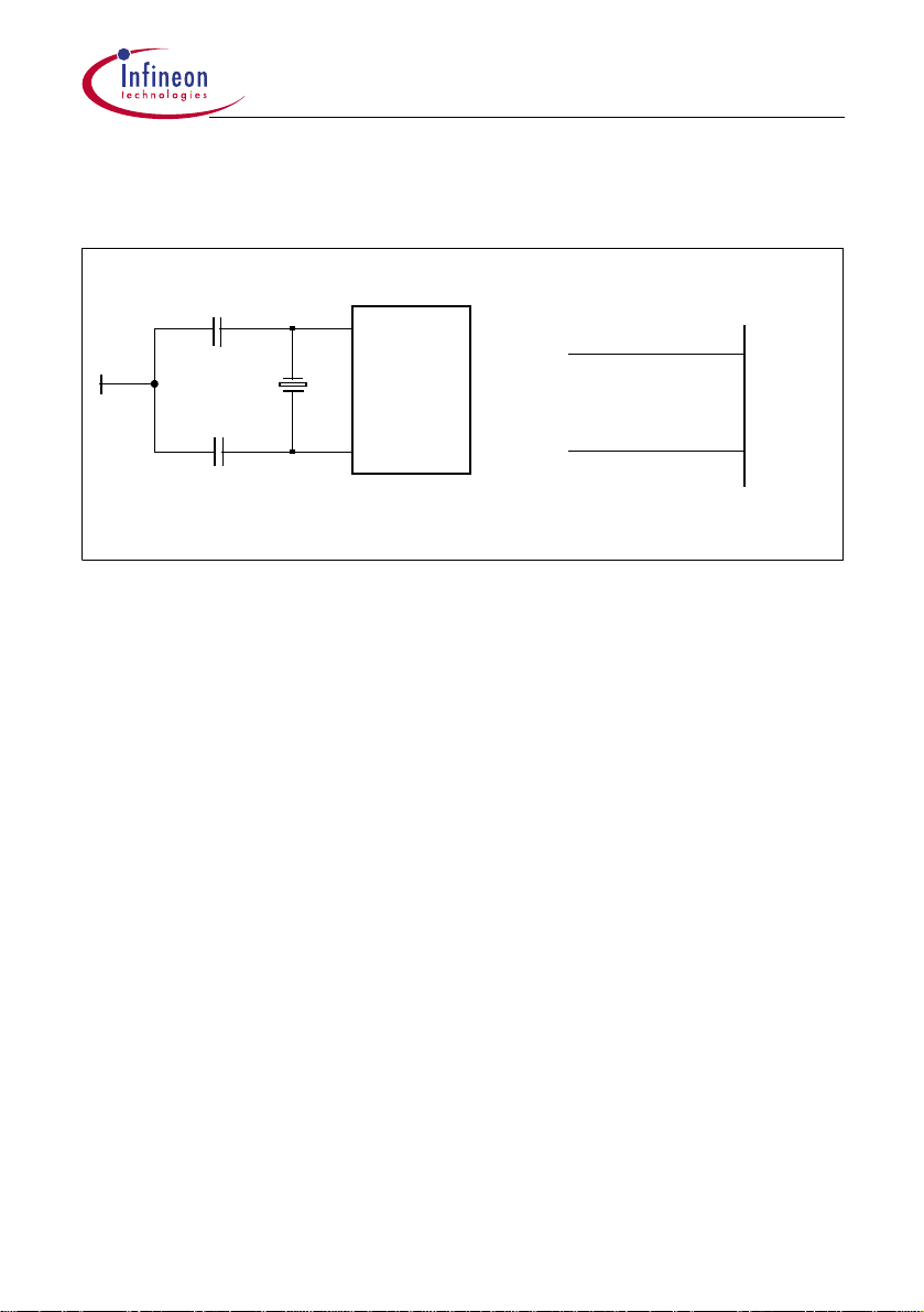
In this application the on-chip oscillator is used as a crystal-controlled, positivereactance oscillator (a more detailed schematic is given in Figure 13). lt is operated in
its fundamental response mode as an inductive reactor in parallel resonance with a
capacitor external to the chip. The crystal specifications and capacitances are noncritical. In this circ uit tbd pF can b e used as single capacitanc e at any freque ncy together
with a good quality crystal. A ceramic resonator can be used in place of the crystal in
cost-critical applications. If a ceramic resonator is used, the two capacitors normally
have different values depending on the oscillator frequency. We recommend consulting
the manufacturer of the ceramic resonator for value specifications of these capacitors.
Data Sheet 23 V 1.0, 2003-05
C868
To internal
timing circuitry
XTAL1
*) Crystal or ceramic resonato r
XTAL2
*)
C
C
1
2
C868
Figure 13 On-Chip Oscillator Circuitry
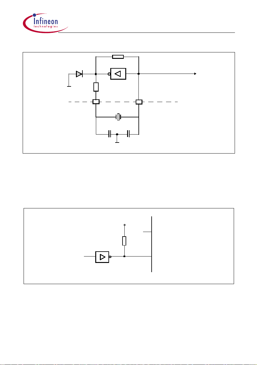
To drive the C868 with an external clock source, the external clock signal has to be
applied to XTA L2, as show n in Figure 14. XTAL1 has to be left unconnected. A pullup
resistor is s ugges ted ( to incr ease t he nois e marg in), bu t is op tion al if VOH of the drivi ng
V
gate corresponds to the
External
Clock
Signal
specification of XTAL2.
IH2
V
DDC
N.C.
C868
XTAL1
XTAL2
Figure 14 External Clock Source
Data Sheet 24 V 1.0, 2003-05
C868
0.1 Special Function Registers
All registers, except the program counter and the four general purpose register banks,
reside in the special function register area. The special function register area consists
of two portions: the standard special function register area and the mapped special
function register area. For accessing the mapped special function area, bit RMAP in
special function register SYSCON0 must be set. All other special function registers are
located in the standard special function register area which is accessed when RMAP is
cleared (“0“).
SYSCON0
System Control Register 0 [Reset value: XX10XXX1
76543210
--EALE RMAP - - - XMAP0
r r rw rw r r r rw
Field Bits Typ Description
RMAP
- [7:2] r reserved;
The functions of the shaded bits are not described here
4rw
Special Function Register Map Control
RMAP = 0 : The access to the non-mapped (standard)
special function register area is enabled.
RMAP = 1 : The access to the mapped special function
register area is enabled.
returns ’0’ if read; should be written with ’0’;
B
]
As long as bit R MA P is s et , th e mapped special fun cti on reg is ter area can be accessed.
This bit is not cleared automatically by hardware. Thus, when non-mapped/mapped
registers are to be accessed, the bi t RMAP must be cleared/se t respectively by softwa re.
The 109 special function registers (SFR) include pointers and registers that provide an
interface between the CP U and the other on-c hip peri pherals. Al l avail able SFRs whose
address bits 0-2 are 0 (e.g. 80H, 88H, 90H, ..., F0H, F8H ) are bit- ad dressabl e. Tot ally
there are 128 directly addressable bits within the SFR area.
All SFRs are list ed in Table 6 and Table 7.In Table 6 they are organized in groups w hich
refer to the functional blocks of the C868-1R, C868-1S. Table 7 illustrates the contents
(bits) of the SFRs
Data Sheet 25 V 1.0, 2003-05

Table 6 Special Function Registers - Functional Blocks
C868
Block Symbol Name Add-
ress
C800
ACC
core
B
DPH
DPL
DPSEL
PSW
SP
SCON
SBUF
IEN0
IEN1
IEN2
IP0
IP1
TCON
TMOD
TL0
TL1
TH0
TH1
PCON
Sys-
PMCON0
tem
CMCON
EXICON
IRCON0
IRCON1
PMCON1
PMCON2
SCUWDT
VERSION
SYSCON0
SYSCON1
1) Bit-addressable special function registers
2) “X“ means that the value is undefined and the location is reserved
3) Register is mapped by bit RMAP in SYSCON0.4=1
4) Register is mapped by bit RMAP in SYSCON0.4=0
Accumulator
B-Register
Data Pointer, High Byte
Data Pointer, Low Byte
Data Pointer Select Register
Program Status Word Register
Stack Pointer
Serial Channel Control Register
Serial Data Buffer
Interrupt Enable Register 0
Interrupt Enable Register 1
Interrupt Enable Register 2
Interrupt Priority Register 0
interrupt Priority Register 1
Timer 0/1 Control Register
Timer Mode Register
Timer 0, Low Byte
Timer 1, Low Byte
Timer 0, High Byte
Timer 1, High Byte
Power Control Register
Wake-up Control Register
Clock Control Register
External Interrupt Control Register
External Interrupt Request Register
Peripheral Interrupt Request Register
Peripheral Management Ctrl Register
Peripheral Management Status Register
SCU/Watchdog Control Register
ROM Version Register
System Control Register 0
System Control Register 1
E0
F0
83
82
84
D0
81
98
99
A8
A9
AA
B8
AC
88
89
8A
8B
8C
8D
87
8E
8F
91
92
93
E8
F8
C0
F9
AD
AF
H
H
H
H
H
H
H
H
H
H
H
H
H
H
H
H
H
H
H
H
H
H
H
H
H
H
H
H
H
H
H
H
Contents
after
Reset
1)
00
H
1)
00
H
00
H
00
H
00
H
1)
00
H
07
H
1)
00
H
00
H
1)
0X000000
XXXXX000
XX0000XX
1)
XX000000
XX000000
1)
00
H
00
H
00
H
00
H
00
H
00
H
0XXX0000
XXX00000
10011111
XXXXXX00
XXXXXX00
XX0000X0
1)
XXXXX000
1)
XXXXX000
1)
X0X00000
00
H
XX10XXX1
00XXX0X0
2)
B
2)
B
2)
B
2)
B
2)
B
2)
B
2)
B
B
2)
B
2)
B
2)
B
2)
B
2)
B
2)
B
2)
B
2)
B
Data Sheet 26 V 1.0, 2003-05

Table 6 Special Function Registers - Functional Blocks (cont’d)
C868
Block Symbol Name Add-
ress
A/D-
ADCON0
Converter
Ports P1
ADCON1
ADDATH
4)
3)
P1DIR
4)
P3
3)
P3DIR
P3ALT
P1ALT
Watch
WDTCON
dog
WDTREL
WDTL
WDTH
Timer 2T2CON
T2MOD
RC2H
RC2L
T2H
T2L
1) Bit-addressable special function registers
2) “X“ means that the value is undefined and the location is reserved
3) Register is mapped by bit RMAP in SYSCON0.4=1
4) Register is mapped by bit RMAP in SYSCON0.4=0
A/D Converter Control Register 0
A/D Converter Control Register 1
A/D Converter Data Register
Port 1 Register
Port 1 Direction Register
Port 3 Register
Port 3 Direction Register
Port 3 Alternate Function Register
Port 1 Alternate Function Register
Watchdog Timer Control Register
Watchdog Timer Reload Register
Watchdog Timer, Low Byte
Watchdog Timer, High Byte
Timer 2 Control Register
Timer 2 Mode Register
Timer 2 Reload/Capture, High Byte
Timer 2 Reload/Capture, Low Byte
Timer 2, High Byte
Timer 2, Low Byte
D8
D9
DB
90
90
B0
B0
B1
B4
A2
A3
B2
B3
C8
C9
CB
CA
CD
CC
H
H
H
H
H
H
H
H
H
H
H
H
H
H
H
H
H
Contents
after
Reset
1)
00
H
XX000000
00
H
1)
FF
1)
FF
1)
FF
1)
FF
00
H
XXX00X00
XXXXXX00
00
H
00
H
00
H
1)
00
H
XXXXXXX0
00
H
00
H
00
H
H
00
H
H
2)
B
H
H
H
H
2)
B
2)
B
2)
B
Data Sheet 27 V 1.0, 2003-05

Table 6 Special Function Registers - Functional Blocks (cont’d)
C868
Block Symbol Name Add-
ress
Capture/
Compare
Unit
T12L
T12H
T13L
T13H
T12PRL
T12PRH
T13PRL
T13PRH
CC60RL
CC60RH
CC61RL
CC61RH
CC62RL
CC62RH
CC63RL
CC63RH
T12DTCL
T12DTCH
CMPSTATL
CMPSTATH
CMPMODIFL
CMPMODIFH
TCTR0L
TCTR0H
TCTR2L
TCTR4L
3)
4)
TCTR4H
ISL
ISH
PISELH
Timer T12 Counter Regi ster, Low By te
Timer T12 Counter Register, High Byte
Timer T13 Counter Regi ster, Low By te
Timer T13 Counter Register, High Byte
Timer T12 Period Register, Low Byte
Timer T12 Period Register, High Byte
Timer T13 Period Register, Low Byte
Timer T13 Period Register, High Byte
Capture/Compare Ch 0 Reg, Low Byte
Capture/Compare Ch 0 Reg, High Byte
Capture/Compare Ch 1 Reg, Low Byte
Capture/Compare Ch 1 Reg, High Byte
Capture/Compare Ch 2 Reg, Low Byte
Capture/Compare Ch 2 Reg, High Byte
T13 Compare Register, Low Byte
T13 Compare Register, High Byte
Timer T12 Dead Time Ctrl, Low Byte
Timer T12 Dead Time Ctrl, High Byte
Compare Timer Status, Low Byte
Compare Timer Status, High Byte
Compare Timer Modificatio n, Low Byte
Compare Timer Modification, High Byte
Timer Control Register 0, Low Byte
Timer Control Register 0, High Byte
Timer Control Register 2, Low Byte
Timer Control Register 4, Low Byte
4)
Timer Control Register 4, High Byte
Cap/Com Interrupt Register, Low Byte
Cap/Com Interrupt Register, High Byte
Port Input Selector Register, High Byte
EC
ED
EE
EF
DE
DF
D2
D3
C2
C3
C4
C5
C6
C7
D4
D5
E6
E7
F4
F5
EA
EB
E2
E3
F2
F2
F3
E4
E5
BB
H
H
H
H
H
H
H
H
H
H
H
H
H
H
H
H
H
H
H
H
H
H
H
H
H
H
H
H
H
H
Contents
after
Reset
00
H
00
H
00
H
00
H
00
H
00
H
00
H
00
H
00
H
00
H
00
H
00
H
00
H
00
H
00
H
00
H
00
H
00
H
00
H
00
H
00
H
00
H
00
H
00
H
00
H
0
H
00
H
00
H
00
H
00
H
1) Bit-addressable special function registers
2) “X“ means that the value is undefined and the location is reserved
3) Register is mapped by bit RMAP in SYSCON0.4=1
4) Register is mapped by bit RMAP in SYSCON0.4=0
Data Sheet 28 V 1.0, 2003-05

Table 6 Special Function Registers - Functional Blocks (cont’d)
C868
Block Symbol Name Add-
ress
Capture/
Compare
Unit
3)
ISSL
3)
ISSH
4)
ISRL
4)
ISRH
3)
INPL
3)
INPH
4)
IENL
4)
IENH
CC60SRL
CC60SRH
CC61SRL
CC61SRH
CC62SRL
CC62SRH
CC63SRL
CC63SRH
MODCTRL
3)
MODCTRH
TRPCTRL
TRPCTRH
PSLRL
MCMOUTL
3)
MCMOUTH
MCMOUTSL
MCMOUTSH
MCMCTRLL
T12MSELL
T12MSELH
Cap/Com Int Status Set Reg, Low Byte
Cap/Com Int Status Set Reg, High Byte
Cap/Com Int Status Rese t Reg, Low Byte
Cap/Com Int Status Reset Reg,High Byte
Cap/Com Int Node Ptr Reg, Low Byte
Cap/Com Int Node Ptr Reg, High Byte
Cap/Com Interrupt Register, Low Byte
Cap/Com Interrupt Register, High Byte
Cap/Com Channel 0 Shadow, Low Byte
Cap/Com Channel 0 Shadow, High Byte
Cap/Com Channel 1 Shadow, Low Byte
Cap/Com Channel 1 Shadow, High Byte
Cap/Com Channel 2 Shadow, Low Byte
Cap/Com Channel 2 Shadow, High Byte
T13 Compare Shadow Reg, Low Byte
T13 Compare Shadow Reg, High Byte
Modulation Control Register, Low By te
3)
Modulation Control Register, High Byte
Trap Control Register, Low Byte
Trap Control Register, High Byte
Passive State Level Register, Low Byte
MCM Output Register, Low Byte
3)
MCM Output Register, High Byte
4)
MCM Output Shadow Regist er, Low Byte
4)
MCM Output Shadow Regis ter,H igh Byte
4)
MCM Control Register, Low Byte
T12 Cap/Com Mode Sel Reg, Low Byte
T12 Cap/Com Mode Sel Reg, High Byte
BC
BD
BC
BD
BE
BF
BE
BF
FA
FB
FC
FD
FE
FF
B6
B7
D6
D7
CE
CF
A6
DC
DD
DC
DD
D6
F6
F7
H
H
H
H
H
H
H
H
H
H
H
H
H
H
H
H
H
H
H
H
H
H
H
H
Contents
after
Reset
00
00
00
00
40
39
00
00
00
00
00
00
00
00
00
00
00
00
00
00
00
00
H
00
H
00
H
00
H
00
00
00
H
H
H
H
H
H
H
H
H
H
H
H
H
H
H
H
H
H
H
H
H
H
H
H
H
H
H
H
1) Bit-addressable special function registers
2) “X“ means that the value is undefined and the location is reserved
3) Register is mapped by bit RMAP in SYSCON0.4=1
4) Register is mapped by bit RMAP in SYSCON0.4=0
Data Sheet 29 V 1.0, 2003-05

Table 7 Contents of the SFRs, SFRs in numeric order of their addresses
Addr Reg-
ister
81
SP 07
H
82
DPL 00
H
83
DPH 00
H
84
DPSEL00
H
Content
after
1)
Reset
H
H
H
H
Bit 7 Bit 6 Bit 5 Bit 4 Bit 3 Bit 2 Bit 1 Bit 0
.7 .6 .5 .4 .3 .2 .1 .0
.7 .6 .5 .4 .3 .2 .1 .0
.7 .6 .5 .4 .3 .2 .1 .0
–––––D2 D1 D0
C868
PCON 0XX0
87
H
0000
88HTCON 00
89
TMOD 00
H
TL0 00
8A
H
8B
TL1 00
H
8C
TH0 00
H
8D
TH1 00
H
8E
PMCON0XXX0
H
0000
8FHCMCON1001
1111
2)
90
P1 FF
H
3)
90
P1DIR FF
H
91
EXICONXXXX
H
XX00
92HIRCON0XXXX
XX00
93
IRCON1XX00
H
00X0
98HSCON 00
99
SBUF 00
H
1) X means that the value is undefined and the location is reserved
2) This register is mapped with RMAP (SYSCON0.4)=0
3) This register is mapped with RMAP (SYSCON0.4)=1
Shaded registers are bit-addressable special function registers
SMOD ––SD GF1 GF0 PDE IDLE
B
TF1 TR1 TF0 TR0 IE1 IT1 IE0 IT0
H
GATE1C/NT1 M1(1) M0(1) GATE0C/NT0 M1(0) M0(0)
H
.7 .6 .5 .4 .3 .2 .1 .0
H
.7 .6 .5 .4 .3 .2 .1 .0
H
.7 .6 .5 .4 .3 .2 .1 .0
H
.7 .6 .5 .4 .3 .2 .1 .0
H
–––EBO BO SDSTATWS EPWD
B
KDIV2 KDIV1 KDIV0 REL4 REL3 REL2 REL1 REL0
B
.7 .6 .5 .4 .3 .2 .1 .0
H
.7 .6 .5 .4 .3 .2 .1 .0
H
––––––ESEL3 ESEL2
B
––––––EXINT3EXINT
B
––INP3 INP2 INP1 INP0 – IADC
B
SM0 SM1 SM2 REN TB8 RB8 TI RI
H
.7 .6 .5 .4 .3 .2 .1 .0
H
2
Data Sheet 30 V 1.0, 2003-05

Table 7 Contents of the SFRs, SFRs in numeric order of their addresses
Addr Reg-
ister
A2HWDTCONXXXX
WDTREL00
A3
H
Content
after
1)
Reset
XX00
H
Bit 7 Bit 6 Bit 5 Bit 4 Bit 3 Bit 2 Bit 1 Bit 0
–––––––WDTI
B
.7 .6 .5 .4 .3 .2 .1 .0
N
C868
PSLRL 00
A6
H
A8HIEN0 0X00
0000
A9HIEN1 XXXX
X000
IEN2 XX00
AA
H
00XX
ACHIP1 XX00
0000
SYSC
AD
H
ON0
AFHSYSC
ON1
2)
B0
P3 FF
H
3)
B0
P3DIR FF
H
B1
P3ALT 00
H
B2
WDTL 00
H
B3
WDTH 00
H
B4
P1ALT XXX0
H
XX10
XXX1
00XX
X0X0
0X00
B6
CC63
H
00
PSL63 – PSL5 PSL4 PSL3 PSL2 PSL1 PSL0
H
EA – ET2 ES ET1 EX1 ET0 EX0
B
–––––EX3 EX2 EADC
B
––EINP3 EINP2 EINP1 EINP0 ––
B
––.5 .4 .3 .2 .1 .0
B
––EALE RMAP –––XMAP
B
ESWC SWC _ _ _ BSLEN_SWAP
B
.7 .6 .5 .4 .3 .2 .1 .0
H
.7 .6 .5 .4 .3 .2 .1 .0
H
CC60 COUT60CC61 COUT61CC62 COUT62CTRAPCOUT
H
.7 .6 .5 .4 .3 .2 .1 .0
H
.7 .6 .5 .4 .3 .2 .1 .0
H
___RxDINT3_EXF2TxD
B
.7 .6 .5 .4 .3 .2 .1 .0
H
SRL
B7HCC63
00
.7 .6 .5 .4 .3 .2 .1 .0
H
SRH
1) X means that the value is undefined and the location is reserved
2) This register is mapped with RMAP (SYSCON0.4)=0
3) This register is mapped with RMAP (SYSCON0.4)=1
Shaded registers are bit-addressable special function registers
0
63
Data Sheet 31 V 1.0, 2003-05

Table 7 Contents of the SFRs, SFRs in numeric order of their addresses
Addr Reg-
ister
B8HIP0 XX00
PISELH00
BB
H
3)
BC
ISSL 00
H
Content
after
1)
Reset
0000
B
H
H
Bit 7 Bit 6 Bit 5 Bit 4 Bit 3 Bit 2 Bit 1 Bit 0
– – .5 .4 .3 .2 .1 .0
––ISPOS
2.1
ISPOS
2.0
ISPOS
1.1
ISPOS
1.0
ISPOS
0.1
ISPOS
0.0
ST12PMST12OMSCC62FSCC62RSCC61FSCC61RSCC60FSCC60
R
2)
BC
H
ISRL 00
RT12PMRT12OMRCC62FRCC62RRCC61FRCC61RRCC60FRCC6
H
0R
3)
BD
ISSH 00
H
– SIDLE SWHE SCHE – STRPFST13PMST13C
H
M
2)
BD
H
ISRH 00
– RIDLE RWHE RCHE – RTRPFRT13PMRT13C
H
M
2)
BE
BE
BF
H
3)
H
2)
H
IENL 00
INPL 00
IENH 00
ENT12PMENT12OMENCC
H
62F
INPCH
H
E.1
– ENIDLEENWHEENCHE– ENTRPFENT13PMENT13
H
INPCH
E.0
INPCC
62.1
ENCC
62R
INPCC
62.0
ENCC
61F
INPCC
61.1
ENCC
61R
INPCC
61.0
ENCC
60F
INPCC
60.1
ENCC
60R
INPCC
60.0
CM
3)
BF
INPH 00
H
C0HSCUWDT00
––INPT1
H
3.1
– PLLR – WDTR WDTEOIWDTDISWDTRSWDTR
H
INPT1
3.0
INPT1
2.1
INPT1
2.0
INPER
R.1
INPER
R.0
E
C2HCC60RL00
.7 .6 .5 .4 .3 .2 .1 .0
H
C868
CC60RH00
C3
H
C4HCC61RL00
CC61RH00
C5
H
1) X means that the value is undefined and the location is reserved
2) This register is mapped with RMAP (SYSCON0.4)=0
3) This register is mapped with RMAP (SYSCON0.4)=1
Shaded registers are bit-addressable special function registers
Data Sheet 32 V 1.0, 2003-05
.7 .6 .5 .4 .3 .2 .1 .0
H
.7 .6 .5 .4 .3 .2 .1 .0
H
.7 .6 .5 .4 .3 .2 .1 .0
H

Table 7 Contents of the SFRs, SFRs in numeric order of their addresses
Addr Reg-
ister
C6HCC62RL00
Content
after
1)
Reset
H
Bit 7 Bit 6 Bit 5 Bit 4 Bit 3 Bit 2 Bit 1 Bit 0
.7 .6 .5 .4 .3 .2 .1 .0
C868
CC62RH00
C7
H
C8HT2CON00
H
H
C9HT2MODXXXX
XXX0
RC2L 00
CA
CB
CC
CD
CE
H
RC2H 00
H
TL2 00
H
TH2 00
H
TRPC
H
00
H
H
H
H
H
TRL
CF
TRPC
H
00
H
TRH
D0HPSW 00
D2
T13PRL00
H
D3HT13PRH00
CC63RL00
D4
H
D5HCC63RH00
H
H
H
H
H
.7 .6 .5 .4 .3 .2 .1 .0
TF2 EXF2 RCLK TCLK EXEN2TR2 C/T2 CP/
–––––––DCEN
B
.7 .6 .5 .4 .3 .2 .1 .0
.7 .6 .5 .4 .3 .2 .1 .0
.7 .6 .5 .4 .3 .2 .1 .0
.7 .6 .5 .4 .3 .2 .1 .0
–––––TRPM2TRPM1TRPM
TRPPENTRPE
TRPEN5TRPEN4TRPEN3TRPEN2TRPEN1TRPE
N13
CY AC F0 RS1 RS0 OV F1 P
.7 .6 .5 .4 .3 .2 .1 .0
.7 .6 .5 .4 .3 .2 .1 .0
.7 .6 .5 .4 .3 .2 .1 .0
.7 .6 .5 .4 .3 .2 .1 .0
RL2
0
N0
2)
MCMC
D6
H
TRLL
3)
D6
MODC
H
TRL
1) X means that the value is undefined and the location is reserved
2) This register is mapped with RMAP (SYSCON0.4)=0
3) This register is mapped with RMAP (SYSCON0.4)=1
Shaded registers are bit-addressable special function registers
Data Sheet 33 V 1.0, 2003-05
00
00
––SWSYN1SWSYN0– SWSEL2SWSEL1SWSE
H
MCMEN– T12M
H
ODEN
5
T12M
ODEN
4
T12M
ODEN
3
T12M
ODEN
2
T12M
ODEN
1
L0
T12M
ODEN
0

Table 7 Contents of the SFRs, SFRs in numeric order of their addresses
Addr Reg-
ister
3)
D7
MODC
H
TRH
D8HADCON000
ADCON1XX00
D9
H
ADDATH00
DB
H
3)
DC
MCMO
H
UTL
2)
MCMO
DC
H
UTSL
3)
DD
MCMO
H
UTH
2)
MCMO
DD
H
UTSH
DE
T12PRL00
H
Content
after
1)
Reset
00
H
H
0000
B
H
00
H
00
H
00
H
00
H
H
Bit 7 Bit 6 Bit 5 Bit 4 Bit 3 Bit 2 Bit 1 Bit 0
ECT13O– T13M
ODEN
5
ADST ADBSYADM1 ADM0 CCU-
T13M
ODEN
4
T13M
ODEN
3
ADEX
T13M
ODEN
2
T13M
ODEN
1
T13M
ODEN
0
ADCH2ADCH1ADCH
0
––ADSTC2ADSTC1ADSTC0ADCTC2ADCTC1ADCT
C0
.7 .6 .5 .4 .3 .2 .1 .0
– RMCMP
5
MCMP4MCMP3MCMP2MCMP1MCMP
0
STRMCM– MCMPS5MCMPS4MCMPS3MCMPS2MCMPS1MCMP
S0
––CURH2CURH1CURH0EXPH2EXPH1EXPH
0
STRHP– CURHS2CURHS1CURHS0EXPHS2EXPHS1EXPH
S0
.7 .6 .5 .4 .3 .2 .1 .0
C868
T12PRH00
DF
H
E0HACC 00
E2
TCTR0L00
H
.7 .6 .5 .4 .3 .2 .1 .0
H
.7 .6 .5 .4 .3 .2 .1 .0
H
CTM CDIR STE12 T12R T12PRET12CLK2T12CLK1T12CL
H
K0
E3
H
TCTR0H10
––STE13 T13R T13PRET13CLK2T13CLK1T13CL
H
K0
E4HISL 00
T12PM T12OMICC62FICC62RICC61FICC61RICC60FICC60
H
R
E5
H
ISH 00
– IDLE WHE CHE TRPS TRPF T13PM T13C
H
M
1) X means that the value is undefined and the location is reserved
2) This register is mapped with RMAP (SYSCON0.4)=0
3) This register is mapped with RMAP (SYSCON0.4)=1
Shaded registers are bit-addressable special function registers
Data Sheet 34 V 1.0, 2003-05

Table 7 Contents of the SFRs, SFRs in numeric order of their addresses
Addr Reg-
ister
E6HT12DTCL00
Content
after
1)
Reset
H
Bit 7 Bit 6 Bit 5 Bit 4 Bit 3 Bit 2 Bit 1 Bit 0
– DTM5 DTM4 DTM3 DTM2 DTM1 DTM0
C868
T12DTCH00
E7
H
E8HPMCON1XXXX
X000
EAHCMPM
00
– DTR2 DTR1 DTR0 – DTE2 DTE1 DTE0
H
– – – – – CCUDIST2DIS ADCDI
B
– MCC63S–––MCC62SMCC61SMCC6
H
ODIFL
EB
H
CMPM
00
– MCC63R–––MCC62RMCC61RMCC6
H
ODIFH
ECHT12L 00
ED
T12H 00
H
EEHT13L 00
EF
T13H 00
H
F0HB 00
2)
F2
TCTR4L00
H
3)
TCTR2L00
F2
H
2)
F3
TCTR4H00
H
F4
CMPS
H
00
.7 .6 .5 .4 .3 .2 .1 .0
H
.7 .6 .5 .4 .3 .2 .1 .0
H
.7 .6 .5 .4 .3 .2 .1 .0
H
.7 .6 .5 .4 .3 .2 .1 .0
H
.7 .6 .5 .4 .3 .2 .1 .0
H
T12STDT12STR––DTREST12REST12RS T12RR
H
– T13TED1T13TED0T13TEC2T13TEC1T13TEC0T13SSCT12SS
H
T13STDT13STR–––T13REST13RS T13RR
H
– CC63ST–––CC62STCC61STCC60S
H
TATL
F5HCMPS
TATH
T12M
F6
H
SELL
F7HT12M
00
00
00
T13IM COUT
H
63PS
MSEL
H
613
––––MSEL
H
MSEL
612
COUT
62PS
MSEL
611
CC62PSCOUT
MSEL
610
SELH
1) X means that the value is undefined and the location is reserved
2) This register is mapped with RMAP (SYSCON0.4)=0
3) This register is mapped with RMAP (SYSCON0.4)=1
Shaded registers are bit-addressable special function registers
61PS
MSEL
603
623
CC61PSCOUT
60PS
MSEL
602
MSEL
622
MSEL
601
MSEL
621
S
0S
0R
C
T
CC60P
S
MSEL
600
MSEL
620
Data Sheet 35 V 1.0, 2003-05

Table 7 Contents of the SFRs, SFRs in numeric order of their addresses
Addr Reg-
ister
F8HPMCON2XXXX
VERSION00
F9
H
Content
after
1)
Reset
X000
H
Bit 7 Bit 6 Bit 5 Bit 4 Bit 3 Bit 2 Bit 1 Bit 0
– – – – – CCUSTT2ST ADCS
B
PROT VER6 VER5 VER4 VER3 VER2 VER1 VER0
T
C868
CC60RL00
FA
H
FBHCC60RH00
CC61RL00
FC
H
FDHCC61RH00
CC62RL00
FE
H
FFHCC62RH00
1) X means that the value is undefined and the location is reserved
2) This register is mapped with RMAP (SYSCON0.4)=0
3) This register is mapped with RMAP (SYSCON0.4)=1
Shaded registers are bit-addressable special function registers
.7 .6 .5 .4 .3 .2 .1 .0
H
.7 .6 .5 .4 .3 .2 .1 .0
H
.7 .6 .5 .4 .3 .2 .1 .0
H
.7 .6 .5 .4 .3 .2 .1 .0
H
.7 .6 .5 .4 .3 .2 .1 .0
H
.7 .6 .5 .4 .3 .2 .1 .0
H
Data Sheet 36 V 1.0, 2003-05

C868
Ports
The C868 has two kinds of po rts. The first kind is pu sh-pull ports in stead of the traditiona l
quasi-bidirectional ports. The ports belonging to this kind are lsb of port 1 which is a 5bit I/O port and port 3 which is an eight-bit I/O port. When configured as inputs, these
ports will be high impedan ce with Sch mitt tri gger featu re. Port 3 is alternate for captu re/
compare functions whereas, port 1 has alternate functions for some of the pins.
The second kind is input ports which are shared by msb of port 1 which is a 3-bit input
port, the interrupts, timer 2 inputs, capture/compare hall inputs and analog inputs.
Data Sheet 37 V 1.0, 2003-05

C868
Timer 0 and 1
Timer 0 and 1 can be used in four operating modes as listed in Table 8:
Table 8 Timer 0 and 1 Operating Modes
Mode Description TMOD System Clock
M1 M0
f
0 8-bit timer with a divide-by-32 prescaler 0 0
1 16-bit timer 0 1
2 8-bit timer with 8-bit autoreload 1 0
3 Timer 0 used as one 8-bit timer and one 8-bit
11
timer
timer 1 stops
The register is incremented every machine cycle. Since the machine cycle consist of
twelve oscillator periods, the count rate is 1/12th of the system frequency. External
inputs INT0 and INT1 can be programmed to function as a gate to facilitate pulse width
measurements. Figure 15 illustrates the input clock logic.
SYS
f
SYS
/(12*32)
/12
f
÷ 12
SYS
C/T = 0
Timer 0/1
Input Clock
Control
INT0
Gate
Pin
=1
TR0
≥1
&
Figure 15 Timer 0 and 1 Input Clock Logic
Data Sheet 38 V 1.0, 2003-05

C868
Timer/Counter 2 with Compare/Capture/Capture
Timer 2 is a 16-bit timer/counter with an up/down count feature. It has three operating
modes:
• 16-bit auto-reload mode (up or down counting)
• 16-bit capture mode
• Baudrate generator
Table 9 Timer/Counter 2 Operating Modes
Mode T2CON T2MOD T2CON T2EX Remarks System
Clock
RCLK
or
TR2 DCEN EXEN Inte-
CP/
RL2
TCLK
16-bit
Autoreload
0010 0 Xreload upon
overflow
0 0 X 0 1 reload trigger
(falling edge)
0011 X 0down counting
0011 X 1up counting
16-bit
Capture
011X 0 X16-bit Timer/
Counter (only
up-counting)
011X 1 capture
T2H,T2L->
RC2H,RC2L
Baudrate
Generator
1X1X 0 Xno overflow
interrupt
request(TF2)
1X1X 1 extra external
interrupt
(“Timer 2“)
off X X 0 X X X Timer 2 stops - -
rnal
f
SYS
/12
f
SYS
/12
f
SYS
/2
T2
max
f
SYS
/24
max
f
SYS
/24
-
Note: denotes a falling edge
Data Sheet 39 V 1.0, 2003-05

C868
Serial Interface (UART)
The serial port is a full duplex port capable of simultaneous transmit and receive
functions. It is also receive-b uffered; it ca n commence re ception of a second by te before
a previously-received byte has been read from the receive register. The serial port can
operate in 3 modes as illustrated in Table 10.
Table 10 UART Operating Modes
Mode SCON Description
SM1 SM0
0 0 0 Reserved
1 0 1 8-bit UART, variable baudrate
10 bits are transmitted (th rough TxD) or rec eived (RxD)
2 1 0 9-bit UART, fixed baudrate
11 bits are transmitted (th rough TxD) or rec eived (RxD)
3 1 1 9-bit UART, variable baudrate
Similar to mode 2, except for the variable baudrate.
For clarification, some terms regarding the difference between “baudrate clock“ and
“baudrate“ should be mentioned.
The serial interface requires a clock rate which is 16 times the baudrate for internal
synchronization. Th erefore, t he b audrate generat ors must p rovi de a “ba udrate c lock“ to
the serial interface which divides it by 16, thereby resulting in the actual “baudrate“.
Data Sheet 40 V 1.0, 2003-05

C868
The baudrates in Mode 1 and 3 are determined by the timer overflow rate. These
baudrates can be det ermined by Timer 1 or by Timer 2 o r both (one for tran smit, the other
for receive.
Table 11 Serial Interface - Baud Rate Dependencies
Serial Interface
Operating Modes
Mode 1 (8-bit UART)
Mode 3 (9-bit UART)
Mode 2 (9-bit UART) – 0 f
1)
Timer 2 functioning as baudrate generator
Active Control Bits Baud Rate Calculation
TCLK/
SMOD
RCLK
0 x Controlled by timer 1 overflow:
1 x Controlled by baud rate generator
1
SMOD
× Timer 1 overflow rate) / 32
(2
SMOD
(2
× Timer 21) overflow rate) / 32
/ 64
SYS
f
/ 32
SYS
Data Sheet 41 V 1.0, 2003-05

C868
Capture/Compare Unit (CCU6)
The CCU6 provides two independent timers (T12, T13), which can be used for PWM
generation, especia lly for AC-m otor cont rol. Additi onally, special control mod es for bl ock
commutation and multi- ph ase mach in es are supported.
Timer 12 Fe atures
• Three capture/compare channels, each channel can be used either as capture or as
compare channel.
• Generation of a three-phase PWM supported (six outputs, individual signals for
highside and lowside switches)
• 16 bit resolution, maximum count frequency = system clock
• Dead-time control for each channel to avoid short-circuits in the power stage
• Concurrent update of the required T12/13 registers
• Center-aligned and edge-aligned PWM can be generated
• Single-shot mode supported
• Many interrupt request sources
• Hysteresis-like control mode
Timer 13 Fe atures
• One independent compare channel with one output
• 16 bit resolution, maximum count frequency = system clock
• Can be synchronized to T12
• Interrupt generation at period-match and compare-match
• Single-shot mode supported
Additional Features
• Block commutation for Brushless DC-drives implemented
• Position detection via Hall-sensor pattern
• Automatic rotational speed measurement for block commutation
• Integrated error handling
• Fast emergency stop without CPU load via external signal (CTRAP
)
• Control modes for multi-channel AC-drives
• Output levels can be selected and adapted to the power stage
• Capture/compare unit can be powerdown in normal, idle and slow-down modes
The timer T12 can work in capture and/or compare mode for its three channels. The
modes can also be co mbined. The tim er T13 can work in com pare mode only . The multichannel control unit generates output patterns which can be modulated by T12 and/or
T13. The modulation sources can be selected and combined for the signal modulation.
Data Sheet 42 V 1.0, 2003-05

Switching Examples
C868
T12clk
T12P
T12P-1
T12P-2
compare-ma tch =
period-match
0
10
active
zero-match
0
0< T12P-3
T12 shadow transfer
1
T12P
T12P-1
T12P-2
compare-match =
period-match
10
passive
active
zero-match
0
0
T12PT12P
T12 shadow transfer
1
T12
CDIR
STE12
CC6x
compare
state
Figure 16 Edge-aligned mode with duty cycles near 100% and near 0%.
Applicable to T13 as well.
T12clk
compare-match
2
1
10
1
0
2
2
compare-match
1
10
1
0
T12
2
CDIR
10
21
passiveactive
T12 shadow transf er
10
01
active
T12 shadow transfer
STE12
CC6x
compare
state
Figure 17 Centre-aligned mode with duty cycles near 100% and near 0%.
Data Sheet 43 V 1.0, 2003-05

C868
Dead-time Generation
The dead-time generation logic is built in a similar way for all three channels of T12.
Each of the three ch ann els w o rks in de pen den tly w it h i ts ow n de ad-t im e c oun ter and the
trigger and enable signals.
T12
Centre-aligned
T12
Edge-aligned
CC6xST
CC6xST
DTCx_o
COUT6x (CC6xPS=0)
CC6x (CC6xPS=0)
Figure 18 Dead-time generation for centre and edge aligned modes
Capture Mode
In capture mode the bits CC6xST indicate the occurrence of the selected capture event
according to the bit fields MSEL6x. A rising and/or a falling edge on the pins CC6x can
be selected as capture event, that is used to transfer the contents of timer T12 to the
CC6xR and CC6xSR registers. In order to wo rk in ca ptu re mod e, the captu re pin s hav e
to be configured as inputs.
Data Sheet 44 V 1.0, 2003-05

C868
Single Shot Mode
In single shot mode, the timer T12 stops automatically at the end of the its counting
period.
edge-aligned mode center-aligned mode
T12P
T12P-1
T12P-2
period-match
while counting up
one-match while
counting down
1
0
T12
T12R
CC6xST
if T12SSC = ’1’
0
T12
T12R
CC6xST
2
if T12SSC = ’1’
Figure 19 Single Shot Mode of T12, T13 is edge-aligned mode only.
Hysteresis-Like Control Mode
The hysteresis-lik e control mode (MSEL6x = ’1001’) offers the possib ility to swi tch off the
PWM output i f the input CCPOSx becomes ’0’. This can be used as a simple motor
control feature by using a comparator indicating e.g. over current.
T12
COUT6x
CC6x
CCPOSx
Figure 20 Hysteresis-like control mode
Data Sheet 45 V 1.0, 2003-05

C868
Synchronization of T13 to T12
The timer T13 can be synchronized on a T12 event. Combined with the single shot
mode, this feature can be used to generate a programmable delay after a T12 event.
5
compare-match while
counting up
T12
0
T13
T13R
2
1
Synchronization of T13 to T12
Multi-channel Mode
The multi-channel mode offers a po ssibility to modulate all six T12-related outp ut signals
within one instruct ion. The bits in bit field MC MP are us ed to sel ect the ou tputs tha t ma y
become active. If the multi-channel mode is enabled (bit MCMEN=’1’), only those
outputs may become ac tive, whi ch hav e a ’1’ at the co rrespon ding bi t posit ion in bi t field
MCMP.
This bit field has its own shadow bit field MCMPS, which can be written by SW. The
transfer of the new value in MCMPS to the bit field MCMP can be triggered by and
synchronized to T12 or T13 eve nts. This structure permit s the SW to write the new value,
which is then tak en in to a cc oun t b y t he H W a t a w ell -def ined moment and synch ronized
to a PWM period. This avoids unintended pulses due to unsynchronized modulation
sources (T12, T13, SW).
4
3
2
1
0
Data Sheet 46 V 1.0, 2003-05

C868
Trap Handling
The trap functionality permits the PWM outputs to react on the state of the input pin
. This functionality can be used to switch off the power devices if the trap input
CTRAP
becomes active (e.g. as emergency stop).
T12
T13
TRPF
TRPS
TRPS
TRPS
CTRAP active
sync. to T13
sync. to T12
no sync.
Figure 21 Trap State Synchronization (with TRM2=’0’)
Data Sheet 47 V 1.0, 2003-05

C868
Modulation control
The modulation control part combines the different modulation sources, six T12-related
signals from the three compare channels, the T13-related signal and the multi-channel
modulation sig nal s. ea ch m odulation source c an b e ind iv idu ally enabled for e ach output
line. Furthermore, the trap funct ionality is taken into account to disable the mo dulation of
the corresponding output line during the trap state (if enabled).
T13
CC60 (MCMP0, no modulation)
COUT60 (MCMP1, no modulation)
CC60 (T12, no modulation)
COUT60 (T12, no modulation)
CC60
(MCMP0 modulated with T12)
COUT60
(MCMP1 modulated with T12)
CC60
(MCMP0 modulated with T12 and 13)
COUT60
(MCMP1 modulated with T12 and T13)
Figure 22 Modulation Control example for CC60 and COUT60.
Data Sheet 48 V 1.0, 2003-05

C868
Hall Sensor Mode
In Brushless-DC motors the next multi-channel state values depend on the pattern of
the Hall inputs. There is a strong correlation between the Hall pattern (CURH) and the
modulation pattern (MCMP). Because of different machine types the modulation
pattern for driving the motor can be different. Therefore it is wishful to have a wide
flexibility in defining the correlation between the Hall pattern and the corresponding
modulation pattern. The CCU6 offers this by having a register which contains the actual
Hall pattern (CURHS), the next expected Hall pattern (EXPHS) and its output pattern
(MCMPS). At ev ery cor re ct H all even t (C HE, se e fi gur e Hall Event Actions) a new Hall
pattern with its correspo ndi ng outp ut p atte rn c an be l oad ed (from a p redefined table) by
software into the register M CMOUTS. Lo ading this shadow regist er can also be done by
a write action on MCMOUTS with bit STRHP = ’1’
The sampling of the Hall patter n (on CCP OSx) is don e with th e T12 clock . By using the
dead-time counter DTC0 (mode MSEL6x= ’1000’) a hardware noise filter can be
implemented to suppress spikes on the Hall inputs due to high di/dt in rugged inverter
environment. In case of a Hall eve nt the DTC0 is relo aded and starts counting. When the
counter value of one is reached, the CCPOSx inputs are sampled (without noise and
spikes) and are compared to the current Hall pattern (CURH) and to the expected Hall
pattern (EXPH). If the sampled pattern equals to the current pattern the edge on
CCPOSx was due to a noise s pike and no ac tion w ill be trig gered (im plic it noise filter). If
the sampled pattern equals to the next expected pattern the edge on CCPOSx was a
correct Hall event, the bit CHE is set which causes an interrupt and the resets T12 (for
speed measurement, see description mode ’1000’ below).
This correct Hall event c an be u se d as a tra ns fer re que st e ve nt fo r regi st er M CMO UTS.
The transfer from MCMOUTS to MCMOUT transfers the new CURH-pattern as well as
the next EXPH-pattern. In case of the sampled Hall inputs were neither the current nor
the expected Hall pattern, the bit WHE (wrong Hall event) is set which also can cause
an interrupt and sets the IDLE mode clearing MCMP (modulation outputs are inactive).
To restart from IDLE the tran sf er req ues t o f MC M OUT S hav e to be i ni tiat ed by software
(bit STRHP and bitfields SWSEL/SWSYN).
Data Sheet 49 V 1.0, 2003-05

C868
Below is a table listing output (MCMP) for a BLDC motor.
Block Commutation Control Table
Mode CCPOS0-
CCPOS2 Inputs
CCP
CCP
CCP
OS0
OS1
OS2
Rotate left,
0° phase shift
1 0 1 inactive inactive active inactive active inactive
1 0 0 inactive inactive active active inactive inactive
1 1 0 inactive active inactive active inactive inactive
0 1 0 inactive active inactive inactive inactive active
0 1 1 active inactive inactive inactive inactive active
0 0 1 active inactive inactive inactive active inactive
Rotate right 1 1 0 active inactive inactive inactive active inactive
1 0 0 active inactive inactive inactive inactive active
1 0 1 inactive active inactive inactive inactive active
0 0 1 inactive active inactive active inactive inactive
0 1 1 inactive inactive active active inactive inactive
0 1 0 inactive inactive active inactive active inactive
Slow down X X X inactive inactive inactive active active active
1)
Idle
1)
In case of the sampled Hall inputs were neither the current nor the expected Hall pattern, the bit WHE (wrong
Hall event) is set which also can cause an interrupt and se ts the IDLE mode clearing MCMP (m odulation
outputs are inactive).
X X X inactive inactive inactive inactive inactive inactive
CC60 - CC62
Outputs
COUT60 - COUT62
Outputs
CC60 CC61 CC62 COUT60COUT61COUT6
2
Data Sheet 50 V 1.0, 2003-05

C868
For Brushless-DC motors there is a special mode (MSEL6x = ’1000b’) which is
triggered by a chang e of the Hall -inputs (CCPOS x). T his mo de sho ws the c apabil ities of
the CCU6. Here T12’s channel 0 acts in capture function, channel 1 and 2 in compare
function (without output modulation) and the multi-channel-block is used to trigger the
output switching together with a possible modulation of T13.
After the detection of a valid Hall edge the T12 count value is captured to channel 0
(representing the actual motor speed) and resets the T12. When the timer reaches the
compare value in channel 1, the next multi-channel state is switched by triggering the
shadow transfer of bit field MCMP (if enabled in bit field SWEN). This trigger event can
be combined with several conditions which are necessary to implement a noise filtering
(correct Hall event) and to synchronize the next multi-channel state to the modulation
sources (avoiding spi kes on the output line s). This compar e function of channel 1 can be
used as a phase delay for the position input to the output switching which is necessary
if a sensorless back -EMF tec hniqu e is us ed ins tead of Hall senso rs. The com pare v alue
in channel 2 can be used as a time-out trigger (interrupt) indicating that the motors
destination spee d is far below the d esired value w hich can be ca used by a abnormal load
change. In this mode the modulation of T12 has to be disabled (T12MODENx = ’0’).
ch0
act. speedCC60
phase delayCC61
timeoutCC62
capture
event resets
T12
gets
captured
value for
act. speed
ch2
for timeout
ch1
compare
for phase delay
compare
CCPOS0
CCPOS1
CCPOS2
CC6x
COUT6y
111
001
1
0
00
11 0
00
0
11
Figure 0-2 Timer T12 Brushless-DC Mode (MSEL6x = 1000)
Data Sheet 51 V 1.0, 2003-05

C868
A/D Converter
The C868 includes a high performance / high speed 8-bit A/D-Converter (ADC) with 5
analog input chann els . It op era tes with a s uc ce ss ive ap prox im ati on t ech ni que and u se s
self calibration mechanisms fo r reduction and compensation of offset and line arity errors.
The A/D converter provides the following features:
– 5 multiplexed input channels, which can also be used as digital inputs
– 8-bit resolution with TUE of +/- 2 LSB8.
– Single or continuous conversion mode
– Start of conversion by software and hardware
– Interrupt request generation after each conversion
– Using successive approximation conversion technique via a capacitor array
– Powerdow n in normal, idle and slow-down modes
The ADC supports two conversion modes - single and continuous conversions. For
each mode, there are two wa ys in whi ch conv ersion ca n be st arted - by softw are and by
the T13PM signal from the CCU module.
Writing a ‘0’ to bit CCU_ADEX select conversion control by ADST. Writing a ’1’ to bit
field ADST starts conversion on the channel that is specified by ADCH. In single
conversion mode, bit field ADM is cleared to ’0’. This is the default mode selected after
hardware re set. When a conve rsion is started , the channel spec ified is sample d. The
busy flag ADBSY is set and ADST is cleared. When the conversion is completed, the
interrupt request signal ADCIRQ is asserted possitively for 2 clocks and the 8-bit result
together with the number of the converted channel is transferred to the result register
ADDATH.
In continuous conversion mode, bit field ADM is set to ’1’. In this mode, the ADC
repeatedly converts the channel specified by ADCH. Bit ADST is cleared at the
beginning of the first conversion. The busy flag ADBSY is asserted until the last
conversion is completed. At the end of each conversion, the interrupt request signal
ADCIRQ will be activated. To stop conversion, ADM has to be reset by software. If the
channel number ADCH is changed while continuous conversion is in progress, the new
channel specified will be sampled in the conversions that follow.
A new request to start conversion will be allowed only after the completion of any
conversion that is in progress.
Writing a ‘1’ to bit CCU_ADEX select conversion control by T13PM trigger signal from
the CCU module.
Note: Caution must be taken when changing conversion start source. To change
conversion source from software to hardware trigger, it is best to let remaining
software conversion to complete before changing. To chan ge co nv ersi on sourc e
from hardware trigger to software, it is best to change source first, let any
Data Sheet 52 V 1.0, 2003-05

C868
remaining hardware conversion to complete before beginning a software
conversion.
Conversion and sample time control
The conversion and sa mple times a re programmed v ia the bit field s ADCTC and ADSTC
respectively of the register ADCON1. Bit field ADCTC (conversion time c ont rol) selects
the internal ADC clock - adc_clk. Bit field ADSTC (sample time control) selects the
sample time.
The total A/D conversion time is given by:
= 2/f
t
ADCC
The sample time tS is configured in p eriods of the selected in ternal ADC clo ck. The tabl e
below lists the possible combinations.
+ tS + 8/adc_clk [5]
SYS
ADCTC Clock
Divider
(TVC)
000 (default) 32 f
001 28 f
010 24 f
011 20 f
100 16 f
101 12 f
110 8 f
111 4 f
ADC Basic Clock
ADSTC Sample Time t
adc_clk
/ 32 000 (default) 2
SYS
/ 28 001 4
SYS
/ 24 010 6
SYS
/ 20 011 8
SYS
/ 16 100 10
SYS
/ 12 101 12
SYS
/ 8 110 14
SYS
/ 4 111 16
SYS
(Periods of
S
adc_clk, STC)
Data Sheet 53 V 1.0, 2003-05

C868
Interrupt System
The C868 provides 13 interrupt vectors with four priority levels. Nine interrupt requests
are generated by the on-chip peripherals (timer 0, timer 1, timer 2, serial channel, A/D
converter, and the capture/compare unit with 4 interrupts) and four interrupts may be
triggered externally.
The wake-up from power-down mode interrupt has a special functionality which allows
the software power-down mode to be terminated by a short negative pulse at pins
CCPOS0/T2/INT0
The 13 interrupt sources ar e divided in to six grou ps. E ach grou p can be prog rammed to
one of the four interrupt priority levels. Additionally, 4 of these interrupt sources are
channeled from 7 Capture/Compare (CCU6) interrupt sources.
Figure 23 to Figure 28 give a general overview of the interrupt sources and illustrate
the request and control flags.
/AN0 or P1.4/RxD.
Data Sheet 54 V 1.0, 2003-05

C868
P3.7/
CC0
P3.5/
CC1
P3.3/
CC2
T12
One Match
T12
Period
Match
T13
Compare
Match
T13
Period Match
P3.1/
CTRAP
Wrong
Hall Event
ICC60R
ISL.0
ICC60F
ISL.1
ICC61R
ISL.2
ICC61F
ISL.3
ICC62R
ISL.4
ICC62F
ISL.5
T12OM
ISL.6
T12PM
ISL.7
T13CM
ISH.0
T13PM
ISH.1
TRPF
ISH.2
WHE
ISH.5
ENCC60R
IENL.0
ENCC60F
IENL.1
ENCC61R
IENL.2
ENCC61F
IENL.3
ENCC62R
IENL.4
ENCC62F
IENL.5
ENT12OM
IENL.6
ENT12PM
IENL.7
ENT13CM
IENH.0
ENT13PM
IENH.1
ENTRPF
IENH.2
ENWHE
IENH.5
≥1
INPL.1
INPL.0
≥1
INPL.2INPL.3
≥1
INPL.4INPL.5
≥1
INPH.2INPH.3
≥1
INPH.4INPH.5
≥1
INPH.0INPH.1
Correct
Hall Event
CHE
ISH.4
ENCHE
IENH.4
INPL.6INPL.7
Capcom Interrupt node 0
Capcom Interrupt node 1
Capcom Interrupt node 2
Capcom Interrupt node 3
Figure 23 Capture/Compare module interrupt structure
Data Sheet 55 V 1.0, 2003-05

INT0_
CORE_N
(CCPOS /
T2 /
/
INT0
AN0)
IT0
TCON.0
IE0
TCON.1
EX0
IEN0.0
0003
C868
Highest
Priority Level
H
Lowest
Priority Level
A/D Converter
Timer 0
Overflow
CCPOS2 /
INT2
/
AN2
ESEL2
EXICON.0
Bit addressable
Request flag is cleared by hardware
IADC
IRCON1.0
TF0
TCON.5
EX2
IRCON0.0
EADC
IEN1.0
ET0
IEN0.1
EX2
IEN1.1
0033
000B
003B
EA
IEN0.7
H
P
o
l
l
IP1.0
IP0.0
i
n
g
S
e
q
u
H
e
n
c
H
IP0.1
IP1.1
Figure 24 Interrupt Structure, Overview Part 1
Data Sheet 56 V 1.0, 2003-05

CCPOS1 /
T2EX /
INT1
/
AN1
P1.3 /
INT3
Capture/compare
interrupt node 0
IT1
TCON.2
ESEL3
EXICON.1
IE1
TCON.3
EXINT3
IRCON0.1
INP0
IRCON1.2
EX1
IEN0.2
EX3
IEN1.2
EINP0
IEN2.2
0013
0043
0083
C868
Priority Level
Highest
H
H
H
Lowest
Priority Level
P
o
l
l
i
n
g
S
e
q
u
e
n
c
IP1.2
EA
IEN0.7
Bit addressable
Request flag is cleared by hardware
IP0.2
Figure 25 Interrupt Structure, Overview Part 2
Data Sheet 57 V 1.0, 2003-05

Timer 1
Overflow
Capture/compare
interrupt node 1
TF1
TCON.7
INP1
IRCON1.3
ET1
IEN0.3
EINP1
IEN2.3
001B
008B
C868
Highest
Priority Level
Lowest
Priority Level
P
o
H
H
l
l
i
n
g
S
e
q
u
e
n
c
IP1.3
EA
IEN0.7
Bit addressable
Request flag is cleared by hardware
IP0.3
Figure 26 Interrupt Structure, Overview Part 3
Data Sheet 58 V 1.0, 2003-05

C868
Highest
Priority Level
Priority Level
UART
Capture/compare
interrupt node 2
SCON.0
SCON.1
RI
TI
IRCON1.4
INP2
P
≥1
0023
ES
IEN0.4
H
o
l
l
i
n
g
S
e
q
EINP2
IEN2.4
0093
H
u
e
n
c
IP1.4
IP0.4
Bit addressable
Request flag is cleared by hardware
EA
IEN0.7
Figure 27 Interrupt Structure, Overview Part 4
Data Sheet 59 V 1.0, 2003-05

C868
Highest
Priority Level
Timer 2
Overflow
Capture/compare
interrupt node 3
TF2
IRCON0.6
INP3
IRCON1.5
ET2
IEN0.5
EINP3
IEN2.5
002B
009B
EA
IEN0.7
H
Priority Level
P
o
l
l
i
n
g
S
e
H
q
u
e
n
c
IP1.5
IP0.5
Bit addressable
Request flag is cleared by hardware
Figure 28 Interrupt Structure, Overview Part 5
Data Sheet 60 V 1.0, 2003-05

Table 12 Interrupt Source and Vectors
C868
Interrupt Source Interrupt Vector
Interrupt Request Flags
Address(core
connections)
External Interrupt 0 0003
Timer 0 Overflow 000B
External Interrupt 1 0013
(EX0) IE0
H
(ET0) TF0
H
(EX1) IE1
H
Timer 1 Overflow 001BH(ET1) TF1
Serial Channel 0023
Timer 2 Overflow 002B
A/D Converter 0033
External Interrupt 2 003B
External Interrupt 3 0043
(ES) RI / TI
H
(EX5) TF2
H
(EX6) IADC
H
(EX7) IEX2
H
(EX8) IEX3
H
004BH(EX9)
0053
(EX10)
H
005B
(EX11)
H
0063
(EX12)
H
006B
(EX13)
H
CAPCOM interrupt node 0 0083
(EX14) INP0
H
CAPCOM interrupt node 1 008BH(EX15) INP1
CAPCOM interrupt node 2 0093H(EX16) INP2
CAPCOM interrupt node3 009BH(EX17) INP3
1)
1)
1)
1)
00A3H(EX18)
00AB
(EX19)
H
00D3
(EX20)
H
00DBH(EX21)
00E3
(EX22)
H
Wake-up from power-down
007B
H
–
mode
1)
Capture/compare has 10 interrupt sources channeled to the 4 interrupt nodes INP0..3. The 3 capture/compare
ports has 3 pairs of interrupt requ est fla gs, IC C60R, ICC60F, ICC61R, ICC61F, ICC62R, ICC62F . The oth er
flags are T12OM, T12PM, T13CM, T13PM, TRPF, WHE, CHE.
Data Sheet 61 V 1.0, 2003-05

C868
lf two or more requests of different priority levels are received simultaneously, the
request of the highest priority is serviced first. lf requests of the same priority level are
received simulta neously, an in ternal polli ng sequen ce determin es which requ est is to be
serviced first. Thus, within each priority level there is a second priority structure
determined by the polling sequence. This is illustrated in Table 13
.
Table 13 Interrupt Source Structure
Interrupt
Group
Priority Bits
of Interrupt
Group
Interrupt Source Priority
High Priority Low
Priority
Priority
0 IP0.0 EXINT0 IADC High
1 IP0.1 TF0 EXINT2
2 IP0.2 EXINT1 EXINT3 INP0
3 IP0.3 TF1 INP1
4 IP0.4 RI + TI INP2
5 IP0.5 TF2 INP3
1)
Capture/compare ha s 10 interrupt sources channele d to the 4 interrupt nodes I NP0..3. The 3 capture/
compare ports has 3 pairs of interrupt request flags, ICC60R, ICC60F, ICC61R, ICC61F, ICC62R, ICC62F.
The other flags are T12OM, T12PM, T13CM, T13PM, TRPF, WHE, CHE.
1)
1)
1)
1)
Low
Within a column, the topmost interrupt is serviced first, then the second and the third,
when available. The interrupt groups are serviced from left to right of the table. A lowpriority interrupt can it self be in terrupte d by a higher-p riority interrupt , but not by an other
interrupt of the same or a lower priority. An interrupt of the highest priority level cannot
be interrupted by another interrupt source.
Data Sheet 62 V 1.0, 2003-05

C868
Fail Save Mechanisms
The C868 offers enhanced fail save mechanisms, which allow an automatic recovery
from software upset or hardware failure :
a programmable watchdog timer (WDT), with variable time-out period from 12.8µs to
f
819.2µs at
Programmable Watchdog Timer
To protect the system against software failure, the user’s program has to clear this
watchdog within a previously programmed time period. lf the software fails to do this
periodical refresh of the watchdog timer, an internal reset will be initiated. The software
can be designed so that the watchdog times out if the program does not work properly.
lt also times out if a software error is based on hardware-related problems.
The watchdo g tim er i n the C 868 is a 16 -bit tim er, w hic h is in crem ent ed by a cou nt rat e
f
/2 upto f
of
SYS
by-two or a divide-by-128 prescaler. The upper 8 bits of the Watchdog Timer can be
preset to a user-program mabl e valu e via a wat chdog servic e access in or der to va ry the
watchdog expire time. The lower 8 bits are reset on each service access. Figure 29
shows the block diagram of the watchdog timer unit.
= 40 MHz.
SYS
/128. The machine cloc k of the C868 is di vided by a presca ler, a divid e-
SYS
WDT
Control
1:2
f
SYS
DISWDT
1:128
MUX
WDTIN
Clear
WDT Low Byte
WDTREL
WDT High Byte
WDTRST
Figure 29 Block Diagram of the Programmable Watchdog Timer
After a reset, the Watchd og Tim er is aut omatical ly ena bled. If i t is dis abled, it c annot be
enabled again during active mode of the device. If the software fails to clear the
watchdog timer an internal reset will be initi ated. The reset cau se (external reset or reset
caused by the watchdog) ca n be ex am in ed b y so ftware (sta tus flag WD TR in SC UWD T
is set). A refresh of the watchdog timer is done by setting bits WDTRE and WDTRS (in
Data Sheet 63 V 1.0, 2003-05

C868
SFR SCUWDT) consecuti vely. This double i nstructio n sequen ce has b een implem ented
to increase system security.
It must be noted, however, that the watchdog timer is halted during the idle mode and
power-down mode of the processor (see section "Power Saving Modes"). It is not
possible to use the idle mode in combination with the watchdog timer function.
Therefore, even the watchdog timer cannot reset the device when one of the power
saving modes has been entered accidentally.
The time period for an overflow of the Watchdog Timer is programmable in two ways :
– the input frequency to the Watchdog Timer can be selected via bit WDTIN in
f
register WDTCON to be either
SYS
/2 or f
– the reload value WDTREL for the hi gh byte of WDT can be progra mmed in register
WDTCON.
SYS
/128.
The period P
between servicing the Watchdog Timer and the next overflow can
WDT
therefore be determined by the following formula:
[0.1]
P
WDT
2
=
* (216 - WDTREL * 28)
f
SYS
(1 +WDTIN*6)
Table 14 lists the poss ib le rang es for the watchdog time w hic h c an be ac hi ev ed usi ng a
certain module clock. Some numbers are rounded to 3 significant digits.
Table 14 Watchdog Time Ranges
Reload value
in WDTREL
Prescaler for
f
SYS
2 (WDTIN = ‘0’) 128 (WDTIN = ‘1’)
40 MHz 20 MHz 16 MHz 40 MHz 20 MHz 16 MHz
FF
7F
00
H
H
H
12.8 µs 25.6 µs 32.0 µs 819.2 µs 1.64 ms 2.05 ms
1.65 ms 3.3 ms 4.13 ms 105.7 ms 211.3 ms 264 ms
3.28 ms 6.55 ms 8.19 ms 209.7 ms 419.4 ms 524 ms
For safety reasons, the user is advised to rewrite WDTCON each time before the
Watchdog Timer is serviced.
Data Sheet 64 V 1.0, 2003-05

C868
Power Saving Modes
The C868 provides two basic power saving modes, the idle mode and the power down
mode. Additionally, a s low down mod e is availabl e. This power sa ving mode red uces the
internal clock rate in normal operating mode and it can also be used for further power
reduction in idle mode.
• Idle Mode
In the idle mode, the oscillator of the C868 continues to run, but the CPU is gated off
from the clock signal. H owever, the interrup t system, the serial p ort, the A/D convert er,
the capture/compare un it, and all timers are further provided with the cloc k. T he CP U
status is preserved in its entirety: the stack pointer, program counter, program status
word, accumulator, and all other registers maintain their data during idle mode.
• Slow Down Mode
In some applications, where power consumption and dissipation are critical, the
controller might run for a certain time at reduced speed (for example, if the controller
is waiting for an input signal). Since in CMOS devices, there is an almost linear
dependence of the operati ng frequ ency and th e pow er supply curren t, so, a reduc tion
of the operating frequency results in reduced power consumption.
• Software Power Down Mode
In the software powe r down mode, the o n-chip oscillato r which operates wi th the XTAL
pins and the PLL are all stopped. Therefore, all functions of the microcontroller are
stopped and only the contents of the on-chip RAM, XRAM and the SFR's are
maintained. The p ort pins, wh ich are c ontrolled by their po rt latches , output t he value s
that are held by their SFR's. The port pins which serve the alternate output functions
show the values they had at the end of the last cycle of the instruction which initiated
the power down mode. ALE is held at logi c low level or high impe dance if dis abled. In
V
the power down mode of operation,
consumption. It must be ensured, however, that
down mode is invoked, and that
V
is restored to its normal operating level before
DDP
the power down mode is terminated.
can be reduced to minimize power
DDP
V
is not reduced before the power
DDP
Data Sheet 65 V 1.0, 2003-05

Table 15 Power Saving Modes Overview
Mode Entering Leaving by Remarks
Idle
Mode
ORL PCON,#01
H
Occurance of any
enabled interrupt
Hardware Reset
CPU clock is stopped;
CPU maintains its
data;
peripheral units are
active (if enabled) an d
provided with clock
Slow
Down
Mode
In normal mode:
ORL PCON,#10
ANL PCON,#0EFH
H
or Hardware Reset
Internal clock rate is
reduced to a
configurable factor of
1
1
/2 to
/32 of the
system clock rate
Software
Power
Down
mode
With idle mode:
ORL PCON,#11
H
With external wake-up
capability from power down
enabled
ORL PMCON0,#01
(to wake-up via pin INT0
H
)
or
ORL PMCON0,#03
H
(to wake-up via pin RxD)
ORL PCON,#02
H
Occurance of any
enabled interrupt to
exit idle mode and
the instruction
ANL PCON,#0EF
to terminate slow
down mode
Hardware Reset
CPU clock is stopped;
CPU maintains all its
data;
Peripheral units are
active (if enabled) an d
H
provided with a
configurable factor of
1
1
/2 to
/32 of the
system clock rate
Hardware Reset Oscillator is stopped;
When INT0
or RxD
goes low for at least
10 µs (latch phase).
Contents of on-chip
RAM and SFR’s are
maintained
But it is desired tha t
the corresponding
pin must be held at
high level during the
power down mode
entry and up to the
wake-up.
With external wake-up
Hardware Reset
capability from power down
disabled
ORL PCON,#02
H
C868
Data Sheet 66 V 1.0, 2003-05

Device Specifications
Absolute Maximum Ratings
Absolute Maximum Rating Parameters
Parameter Symbol Limit Values Unit Notes
min. max.
Ambient temperature under bias
Storage temperature
Voltage on
to ground (
V
pins with respect
DDP
V
)
SSP
Voltage on any pin except int/
T
T
V
V
A
STG
DDP
IN0
-40 125 °C
-65 150 °C-
-0.3 4.6 V -
-0.5 4.6 V analog and XTAL with respect to
ground (V
Voltage on any int/analo g pin with
respect to ground (
Voltage on XTAL pins with
respect to ground (
Input current on any pin during
SSP
)
V
V
SSP
SSC
V
IN1
)
V
IN2
)
Ι
OV
-0.5 4.6 V -
-0.5 4.6 V -
-10 10 mA -
1)
overload condition
Absolute sum of al l inp ut currents
Σ|ΙOV|- 43 mA-
during overload condi tion
Power dissipation P
1)
Proper operation is not guaranteed if overload conditions occur on functional pins like XTAL2 etc.
DISS
-tbdW-
C868
Note: Stresses above those listed under “Absolute Maximum Ratings” may cause
permanent damage to the device. This is a stress rating only and functional
operation of the device at these or any other conditions above those indicated in
the operational sections of this specification is not implied. Exposure to absolute
maximum rating conditions for extended periods may affect device reliability.
During absolute maximum rating overload conditions (
V
IN2>VDDC
or V
IN2<VSSC
) the voltage on V
pin with respect to ground (V
DDP
V
IN>VDDP
or VIN<V
SSP
SSP
must not exceed the values defined by the absolute maximum ratings.
Data Sheet 67 V 1.0, 2003-05
,
)

C868
Operating Conditions
The following operating conditions must not be exceeded in order to ensure correct
operation of the C868. All parameters specified in the following sections refer to these
operating conditions, unless otherwise noticed.
Operating Condition Parameters
Parameter Symbol Limit Values Unit Notes
min. max.
Digital supply voltage
Digital ground
V
DDP
V
SSC,VSSP
voltages
Ambient temperature T
Analog reference
V
A
AREF
voltage
Analog ground
V
AGND
voltage
Analog input voltage
External Clock
Input current on any
V
f
OSC
Ι
OV0
AIN
pin during overload
condition except int/
analog and XTAL
int/analog pin Ι
XTAL pin Ι
Absolute sum of all
ΣΙ
OV1
OV2
OV
input currents during
overload condition
Notes:
1)
Oscillator or external clock disabled.
2)
Overload conditions u nder operating conditions occur if the voltage on the respective pin exceeds the
specified operating range (i.e.
on all port pins may not exceed 20mA. The suply voltages
limits.
3)
Not 100% tested, but guaranteed by design characterization.
V
OV
3.0 3.6 V Ac ti ve mo de,
tbd 3.6 V PowerDown
0V-
-40 85 °C SAF-C868...
-40 125 °C SAK-C868...
3.0V V
DDP
+
V-
0.1
V
SSP
- 0.1 V
SSP
+
V-
0.1
V
AGND
V
AREF
V-
6.67 10.67 MHz -
-5 5 mA -
-2 5 mA -
-5 5 mA -
-|20|mA-
> V
+0.5V or V
DDP
OV
< V
-0.5V). The absolute sum of input currents
SSP
V
DDP
and V
must remain within the specified
SSP
f
SYSmax
mode
2)3)
3)4)
3)5)
3)
= 40 MHz
1)
Data Sheet 68 V 1.0, 2003-05

4)
Overload conditions u nder operating conditions occur if the voltage on the respective pin exceeds the
specified operating ra nge (i.e.
port pins may not exceed 20mA. The suply voltages
5)
Overload conditions u nder operating conditions occur if the voltage on the respective pin exceeds the
specified operating range (i.e.
on all port pins may not exceed 20mA. The suply voltages
limits.
V
OV
V
OV
> tbd or V
> V
DDC
< V
OV
+0.5V or V
-0.5V). The absolu te sum of input cu rrents o n all
SSC
V
and V
DDP
OV
< V
must remain within the specified limits.
SSP
-0.5V). The absolute sum of input currents
SSC
V
DDP
and V
must remain within the specified
SSP
C868
Data Sheet 69 V 1.0, 2003-05

C868
DC Characteristics
(Operating Conditions apply )
Parameter Symbol Limit Values Unit Test Condition
min. max.
Input low voltages
all except XTAL2, int/analog
i
nt/analog
XTAL2
V
IL0
V
IL1
V
IL2
-0.5
-0.5
-0.5
0.3V
0.3V
0.1V
DDP
DDC
DDC
Input high voltages
all except XTAL2, int/analog
int/analog
XTAL2
Output low voltage
V
IH0
V
IH1
V
IH2
V
OL
0.7V
0.7V
0.7V
– 0.45 V SAF-C868...
DDP
DDC
DDC
V
V
V
DDP
DDP
DDC
+0.5
+0.5
+0.5
– 0.55 V SAK-C868...
Output high voltage
Input leakage current (all
V
OH
I
LI0
2.4 – VIOH=10mA
– ±0.5uA0.4<V
except int/analog)
Input leakage current (int/
I
LI1
– ±0.5uA0.4<V
analog)
Input low current (XTAL2) I
Digital supply voltage V
Blocking capacitor for
V
DDC
Pin capacitance C
LI2
DDC
IO
– ±10 uA 0.4<VIN<V
3)
2.25
2.75 V –
136 470 nF –
-10pFfC = 1MHz
Note:
1)
Interrupt/analog p ins are input only and has CMOS characteristics whereas th e other I/O pins have TTL
characteristics.
2)
The leakage curr ent of interrupt/analog pi n s d epe nd s on the leakage cu rre nt of the CMOS pad fo r the digital
functions and the analog pad.
3)
The V
Microcontroller in power down mode;RESET = V
V
connected to gnd; 20mA current sourced from the V
4)
Ceramic type (±20%) max ESR: 25mΩ ,max trace length to capacitor is 10mm.
is measured under the following conditions:
DDC
; RxD/INT0 = V
DDP
; all other pins ar e set to input and connected t o gnd; ALE output disabled and
DDP
; XTAL2 = V
DDP
DDC
pin.
; XTAL1 = N.C.; V
SSC
1)
–
V
V
V
–
V
V
V
=10mA
I
OL
I
=10mA
OL
IN<VDDP
IN<VDDP
DDC
4)
T
= 250C
A
= V
SSP
; V
AREF
AGND
2)
=
Data Sheet 70 V 1.0, 2003-05

C868
Power Supply Current
Parameter Symbol Limit Values Unit Test Condition
Active
mode
C868-1S 40
MHz
C868-1R 40
MHz
Idle mode C868-1S 40
MHz
C868-1R 40
MHz
Active
mode with
slow-down
enabled
Idle mode
with slowdown
enabled
Power-
C868-1S 40
MHz
C868-1R 40
MHz
C868-1S 40
MHz
C868-1R 40
MHz
C868-1S
down mode
C868-1R I
Note:
1)
The typical I
values are periodically measured at TA = + 25 °C but not 100% tested.
DDP
1)
typ.
I
DDP
3)
I
DDP
3)
I
DDP
3)
I
DDP
3)
I
DDP
3)
I
DDP
3)
I
DDP
3)
I
DDP
3)
I
PDP
13.1 15.6 mA
13.5 15.5 mA
7.8 9.6 mA
7.9 9.1 mA
3.5 4.4 mA
3.6 4.1 mA
3.4 4.2 mA
3.6 4.1 mA
240 300 uA SAF-C868...
240 400 uA
PDP
240 300 uA
240 400 uA
max.
2)
4)
5)
6)
7)
8)
SAK-C868...
SAF-C868...
SAK-C868...
8)
8)
8)
2)
The maximum I
3)
System clock, set by using external clock of 10.67MHz and setting KDIV in CMCON to 010 (factor of 4)
4)
I
(active mode) is measured with:
DDP
XTAL2 driven with tR, tF=5ns, V
RESET
= V
(approx. 1 mA).
values are measured under worst case conditions (TA = – 40 °C and V
DDP
= V
; all other pins are disconnected . ?I
DDP
IL1,VIL2
+0.5V, V
SSP
would be slightly higher if the crystal oscillator is used
DDP
IH1,VIH2
= V
– 0.5 V; XTAL1 = N.C.;
DDP
DDP
=3.6V).
Data Sheet 71 V 1.0, 2003-05

5)
I
(idle mode) is measured with all output pins disconnected and with all peripheral disabled:
DDP
XTAL2 driven with tR, tF=5ns, V
RESET
= V
; all other pins are disconnected.
DDP
6)
I
(active mode with slow down mode) is measured with all output pins disconnected:
DDP
XTAL2 driven with tR, tF=5ns, V
RESET
= V
; all other pins ar e disconnecte d; the mi crocontrol ler is pu t into slow-do wn mode by software
with the slow-down clock set to 1/32 of system clock.
7)
I
DDP
disabled:
DDP
(idle mode with slow do wn mode ) is measure d with al l output pi ns disconn ected and wit h all peri pheral
XTAL2 driven with tR, tF=5ns, V
RESET
= V
; all other pins ar e disconnecte d; the mi crocontrol ler is pu t into slow-do wn mode by software
with the slow-down clock set to 1/32 of system clock.
8)
I
PDC
RESET = V
are set to input and connected to gnd; ALE output disabled and connected to gnd.
DDP
and I
(power-down mode) are measured under the following condit ions:
PDP
; XTAL2 = V
DDP
; XTAL1 = N.C.; V
SSC
IL1,VIL2
IL1,VIL2
IL1,VIL2
= V
= V
= V
SSP
SSP
SSP
+0.5V, V
+0.5V, V
+0.5V, V
= V
AGND
IH1,VIH2
IH1,VIH2
IH1,VIH2
SSP
; V
AREF
= V
– 0.5 V; XTAL1 = N.C.;
DDP
= V
– 0.5 V; XTAL1 = N.C.;
DDP
= V
– 0.5 V; XTAL1 = N.C.;
DDP
= V
; RxD/INT0 = V
DDP
; all other pins
DDP
C868
Data Sheet 72 V 1.0, 2003-05

Power Supply Current Calculation Formulae
Parameter Symbol Formula
Active mode C868-1S I
C868-1R I
Idle mode C868-1S I
C868-1R I
Active mode with
C868-1S I
slow-down enabled
C868-1R I
Idle mode with slow-
C868-1S I
down enabl ed
C868-1R I
1)
f
is in MHz and results in mA.
SYS
DDP
I
DDP
DDP
I
DDP
DDP
I
DDP
DDP
I
DDP
DDP
I
DDP
DDP
I
DDP
DDP
I
DDP
DDP
I
DDP
typ
max
typ
max
typ
max
typ
max
typ
max
typ
max
typ
max
typ
max
0.25* f
0.26 *
0.27* f
0.29 *
0.13* f
0.13 *
0.13* f
0.15 *
0.01 * f
0.02 *
0.01 * f
0.01 *
0.01* f
0.01 *
0.02* f
0.02 *
SYS
f
SYS
f
SYS
f
SYS
f
f
f
SYS
f
SYS
f
1)
SYS
SYS
SYS
SYS
SYS
SYS
SYS
SYS
SYS
SYS
C868
+ 3.1
+ 5.2
+ 2.7
+ 3.9
+ 2.6
+ 4.0
+ 3.7
+ 3.1
+ 3.1
+ 3.6
+ 3.2
+ 3.7
+ 3.0
+ 3.8
+ 2.8
+ 3.3
Data Sheet 73 V 1.0, 2003-05

A/D Converter Characteristics
(Operating Condition Parameters)
Parameter Symbol Limits Unit Test Condition
min max
Analog input voltage
Sample time
Conversion cycl e time
Total unadjusted error
ADC input resistance
ADC input capacitance
ADC reference pin
capacitance
V
AIN
t
S
t
ADCC
T
UE
R
AIN
C
AIN
C
AREF
V
AGND
64*t
52*t
48*t
40*t
32*t
24*t
16*t
8*t
SYS
322*t
282*t
242*t
202*t
162*t
122*t
82*t
42*t
SYS
SYS
SYS
SYS
SYS
SYS
SYS
SYS
SYS
SYS
SYS
SYS
SYS
SYS
SYS
V
AREF
512*t
448*t
384*t
320*t
256*t
192*t
128*t
64*t
770*t
674*t
578*t
482*t
386*t
290*t
194*t
98*t
SYS
SYS
SYS
SYS
SYS
SYS
SYS
SYS
SYS
SYS
SYS
SYS
SYS
SYS
SYS
SYS
– ±2
±3
– 1.5 kΩ
– 10 pF
– 40 pF
1)
V
ns Prescaler/32
Prescaler/28
Prescaler/24
Prescaler/20
Prescaler/16
Prescaler/12
Prescaler/8
Prescaler/4
ns Prescaler/32
Prescaler/28
Prescaler/24
Prescaler/20
Prescaler/16
Prescaler/12
Prescaler/8
Prescaler/4
LSB V
V
4)5)
5)
5)
AGND
AGND
≤ V
≤ V
AIN
AIN
≤ V
≤ V
Note:
1)
V
may exceed V
AIN
cases will be 00
2)
T
(max.) is tested at – 20 ≤ TA≤ 125 °C; V
UE
by design characterization for all other voltages within the defined voltage range.
3)
T
(max.) is tested at – 40 ≤ TA< – 20 °C; V
UE
by design characterization for all other voltages within the defined voltage range.
or FFH, respectively.
H
AGND
or
V
AREF
up to the maximum ratings. However, the conversion result in these
= 3.3 V; V
DDP
DDP
≤ 3.3 V; V
AREF
AREF
= V
= V
DDP
V and V
and V
DDP
SSP
SSP
= V
= V
AGND
AGND
. It is guaranteed
. It is guaranteed
C868
AREF
AREF
2)
3)
Data Sheet 74 V 1.0, 2003-05

4)
During the sample time the inpu t capacitance C
internal resistance of the analog source must allow the capacitance to reach their final voltage level within
After the end of the sample time
5)
Not 100% tested, but guaranteed by design characterization.
t
, changes of the analog input voltage have no effect on the conversion result.
S
must be charged/discharged by the external source. The
AIN
C868
t
.
S
Data Sheet 75 V 1.0, 2003-05

Clock calculation table for ADC
1)
TVC
2)
STC
t
ADCC
t
S
TVC
STC
t
ADCC
t
S
TVC
STC
t
ADCC
t
S
1)
2)
1)
2)
246810121416
322 386 450 514 578 642 706 770
64 128 192 256 320 384 448 512
246810121416
282 338 394 450 506 562 618 674
56 112 168 224 280 336 392 448
246810121416
242 290 338 386 434 482 530 578
48 96 144 192 240 288 336 384
32
28
24
t
ADC
t
SYS
t
SYS
t
ADC
t
SYS
t
SYS
t
ADC
t
SYS
t
SYS
C868
3)
3)
3)
1)
TVC
2)
STC
t
ADCC
t
S
1)
TVC
2)
STC
t
ADCC
t
S
1)
TVC
2)
STC
t
ADCC
t
S
Data Sheet 76 V 1.0, 2003-05
246810121416
202 242 282 322 362 402 442 482
40 80 120 160 200 240 280 320
246810121416
162 194 226 258 290 322 354 386
32 64 96 128 160 192 224 256
246810121416
122 146 170 194 218 242 266 290
24 48 72 96 120 144 168 192
20
16
12
t
ADC
t
SYS
t
SYS
t
ADC
t
SYS
t
SYS
t
ADC
t
SYS
t
SYS
3)
3)
3)

1)
TVC
2)
STC
t
ADCC
t
S
1)
TVC
2)
STC
t
ADCC
t
S
1)
TVC is the clock divider specified by bit fields ADCTC.
2)
STC is the sample time control specified by bit fields ADSTC.
3)
t
ADC
246810121416
82 98 114 130 146 162 178 194
16 32 48 64 80 96 112 128
246810121416
42 50 58 66 74 82 90 98
8 16243240485664
is t
*TVC
SYS
C868
8
3)
t
ADC
t
SYS
t
SYS
4
3)
t
ADC
t
SYS
t
SYS
Data Sheet 77 V 1.0, 2003-05

C868
AC Characteristics
(Operating Condition Apply)
External Clock Drive Characteristics
Parameter Symbol Limit Values Unit
Variable Ext Clock
6.67 to 10.67 MHz
min max
Oscillating period
High time
Low time
Rise time
Fall time
t
OSC
t
1
t
2
t
R
t
F
ALE Characteristics
Parameter Symbol Limit Values Unit
ALE pulse width
ALE period
t
AWD
t
ACY
93.75 150 ns
46.875 75 ns
46.875 75 ns
-10ns
-10ns
System freq = 6.25MHz to 40MHz
Duty Cycle 0.5
min max
50 320 ns
150 960 ns
Data Sheet 78 V 1.0, 2003-05

C868
t
1
t
2
t
OSC
Figure 30 External Clock Drive on XTAL2
t
AWD
t
ACY
Figure 31 ALE Characteristic
t
R
t
F
0.7 V
c
DD
0.2 VDD - 0.1
c
MCT04105
Data Sheet 79 V 1.0, 2003-05

Package Outlines
Plastic Package, P-DSO-28-1 for SAF-C868-1RG BA, SAF-C868-1SG BA
SAF-C868A-1RG BA, SAF-C868A-1SG BA and SAF-C868P-1SG BA,
SAK-C868-1RG BA, SAK-C868-1SG BA, SAK-C868A-1RG BA,
SAK-C868A-1SG BA and SAK-C868P-1SG BA.
0.35 x 45˚
0.35
1.27
+0.15
-0.2
-0.1
2.45
2.65 MAX.
0.2
2)
28x0.2
0.1
7.6
0.4
10.3
-0.2
1)
+0.8
±0.3
+0.09
0.23
C868
MAX.8˚
28
1
18.1
-0.4
15
14
1)
Index Marking
1)
Does not include plastic or metal protrusion of 0.15 max. per side
2)
Does not include dambar protrusion of 0.05 max. per side
Figure 32 DSO-28-1 Package Outlines
Data Sheet 80 V 1.0, 2003-05

Plastic Package, P-TSSOP-38-1 for SAF-C868-1RR BA,
SAF-C868-1SR BA, SAF-C868A-1RR BA, SAF-C868A-1SR BA,
SAF-C868P-1SR BA, SAK-C868-1RR BA, SAK-C868-1SR BA,
SAK-C868A-1RR BA, SAK-C868A-1SR BA, and SAK-C868P-1SR BA.
3)
±0.1
4.4
±0.05
-0.2
+0.05
0.1
1
1.2 MAX.
0.5
+0.07
2)
0.2
-0.03
38
1
±0.1
9.7
Index Marking
1)
Does not include plastic or metal protrusion of 0.15 max. per side
2)
Does not include dambar protrusion of 0.08 max. per side
3)
Does not include plastic or metal protrusion of 0.25 max. per side
0.08
19
1)
C
M
A
C
38x
0.1
0.6
6.4
20
A
B
+0.075
-0.035
0.125
±0.15
0.2 B
C868
...8˚0˚
38x
Figure 33 TSSOP-38-1 Package Outlines
Data Sheet 81 V 1.0, 2003-05

Infineon goes for Business Excellence
“Business excellence means intelligent approaches and clearly
defined processes, which are both constantly under review and
ultimately lead to good operating results.
Better operating results and business excellence mean less
idleness and wastefulness for all of us, more professional
success, more accurate information, a better overview and,
thereby, less frustration and more satisfaction.”
Dr. Ulrich Schumacher
http://www.infineon.com
Published by Infineon Technologies AG
 Loading...