


Data Sheet, Feb. 2003
C515C
8-Bit Single-Chip Microcontroller
Microcontrollers
Never stop thinking.

Edition 2003-02
Published by Infineon Technologies AG,
St.-Martin-Strasse 53,
81669 München, Germany
© Infineon Technologies AG 2003.
All Rights Reserved.
Attention please!
The information herein is given to describe certain components and shall not be considered as a guarantee of
characteristics.
Terms of delivery and rights to technical change reserved.
We hereby disclaim any and all warranties, including but not limited to warranties of non-infringement, regarding
circuits, descriptions and charts stated herein.
Information
For further information on technology, delivery terms and conditions and prices please contact your nearest
Infineon Technologies Office in Germany or our Infineon Technologies Representatives worldwide
(www.infineon.com).
Warnings
Due to technical requirements components may contain dangerous substances. For information on the types in
question please contact your nearest Infineon Technologies Office.
Infineon Technologies Components may only be used in life-support devices or systems with the express written
approval of Infineon Technologies, if a failure of such components can reasonably be expected to cause the failure
of that life-support device or system, or to affect the safety or effectiveness of that device or system. Life support
devices or systems are intended to be implanted in the human body, or to support and/or maintain and sustain
and/or protect human life. If they fail, it is reasonable to assume that the health of the user or other persons may
be endangered.

Data Sheet, Feb. 2003
C515C
8-Bit Single-Chip Microcontroller
Microcontrollers
Never stop thinking.

C515C Data Sheet
Revision History: 2003-02
Previous Version: 2000-08
Page Subjects (major changes since last revision)
Enhanced Hooks Technology™ is a trademark of Infineon Technologies.
We Listen to Your Comments
Any information within this document that you feel is wrong, unclear or missing at all?
Your feedback will help us to continuously improve the quality of this document.
Please send your proposal (including a reference to this document) to:
mcdocu.comments@infineon.com
Features
• Full upward compatibility with SAB 80C515A
• On-chip program memory (with optional memory protection)
– C515C-8R 64 Kbytes on-chip ROM
– C515C-8E 64 Kbytes on-chip OTP
– alternatively up to 64 Kbytes external program memory
• 256 bytes on-chip RAM
• 2 Kbytes of on-chip XRAM
• Up to 64 Kbytes external data memory
• Superset of the 8051 architecture with 8 datapointers
• Up to 10 MHz external operating frequency (1
external clock)
• On-chip emulation support logic (Enhanced Hooks Technology)
• Current optimized oscillator circuit and EMI optimized design
µs instruction cycle time at 6 MHz
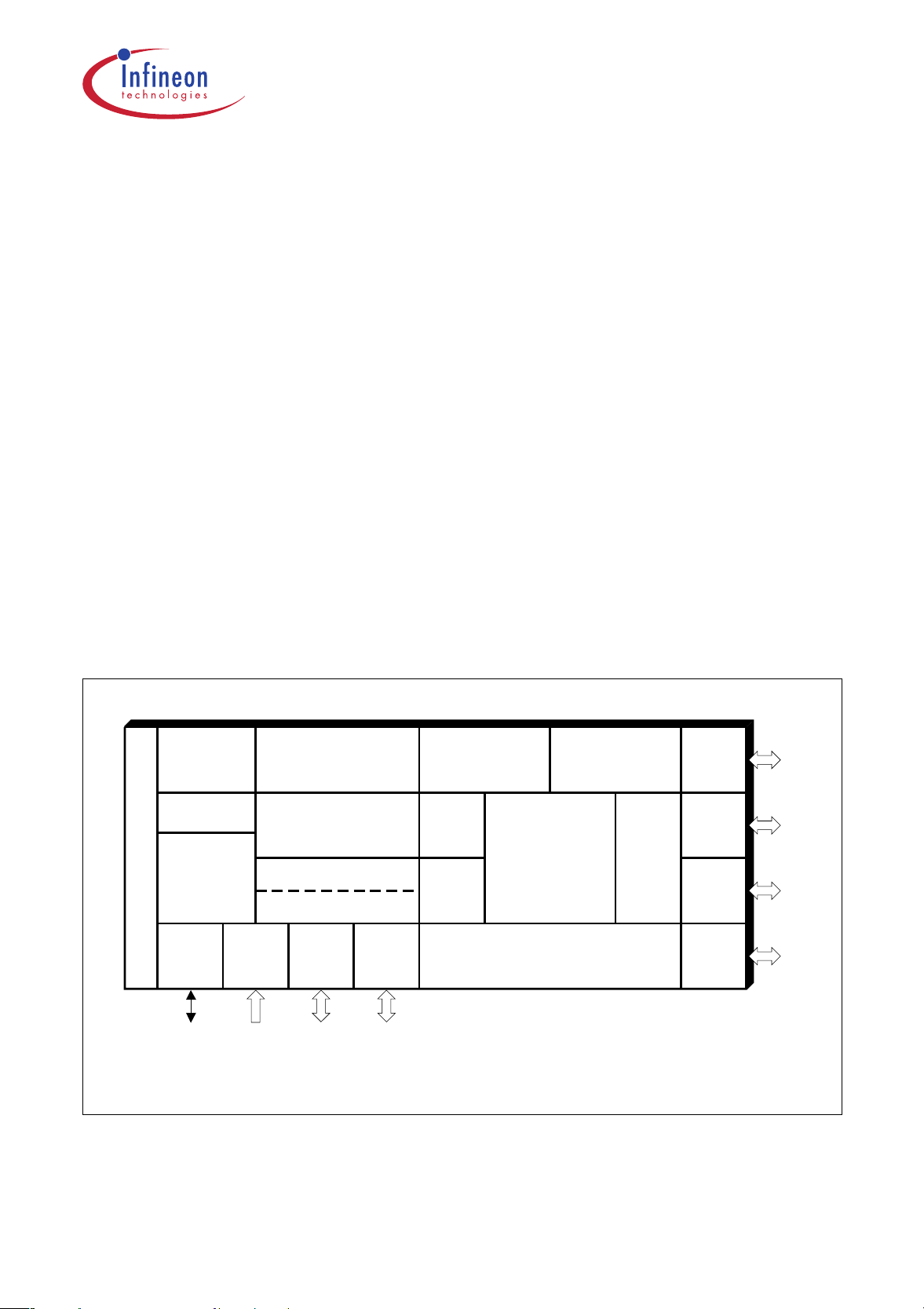
C515C8-Bit Single-Chip Microcontroller
(further features are on next page)
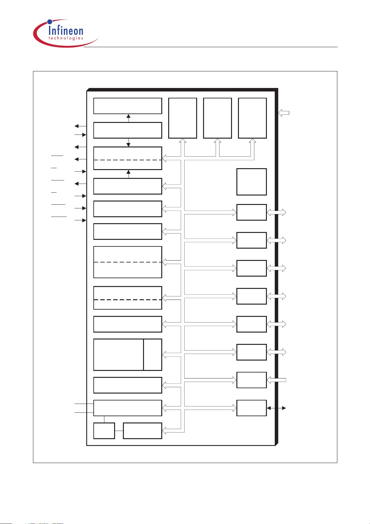
SSC (SPI)
Interface
Oscillator
Watchdog
Power
Save Modes
Idle/
Power down
Slow down
On-Chip Emulation Support Module
Port 7 Port 6 Port 5 Port 4
I/O I/O I/OAnalog/
Digital
Input
Full-CAN
Controller
10 Bit ADC
(8 inputs)
Timer 2
Capture/Compare Unit
XRAM
2k x 8
T0
CPU
8 Datapointer
T1
Program Memory
C515C-8R : 64k x 8 ROM
C515C-8E : 64k x 8 OTP
RAM
256 x 8
USART
Port 0
Port 1
Bit8
Port 2
Port 3
I/O
I/O
I/O
I/O
MCA03646
Figure 1 C515C Functional Units
Data Sheet 1 2003-02

• Eight ports: 48 + 1 digital I/O lines, 8 analog inputs
– Quasi-bidirectional port structure (8051 compatible)
– Port 5 selectable for bidirectional port structure (CMOS voltage levels)
• Full-CAN controller on-chip
– 256 register/data bytes are located in external data memory area
– max. 1 MBaud at 8 - 10 MHz operating frequency
• Three 16-bit timer/counters
– Timer 2 can be used for compare/capture functions
• 10-bit A/D converter with multiplexed inputs and built-in self calibration
• Full duplex serial interface with programmable baudrate generator (USART)
• SSC synchronous serial interface (SPI compatible)
– Master and slave capable
– Programmable clock polarity/clock-edge to data phase relation
– LSB/MSB first selectable
– 2.5 MHz transfer rate at 10 MHz operating frequency
• Seventeen interrupt vectors, at four priority levels selectable
• Extended watchdog facilities
– 15-bit programmable watchdog timer
– Oscillator watchdog
• Power saving modes
–Slow-down mode
– Idle mode (can be combined with slow-down mode)
– Software power-down mode with wake-up capability through INT0
or RXDC pin
– Hardware power-down mode
• CPU running condition output pin
• ALE can be switched off
• Multiple separate
V
DD/VSS
pin pairs
• P-MQFP-80-1 package
• Temperature Ranges:
SAB-C515C versions:
SAF-C515C versions:
SAH-C515C versions:
Note: Versions for extended temperature range -40
T
= 0 to 70 °C
A
T
= -40 to 85 °C
A
T
= -40 to 110 °C
A
°C to 110 °C (SAH-C515C) are
available on request.
C515C
The C515C is an enhanced, upgraded version of the SAB 80C515A 8-bit microcontroller
which additionally provides a full CAN interface, a SPI compatible synchronous serial
interface, extended power save provisions, additional on-chip RAM, 64K of on-chip
program memory, two new external interrupts and RFI related improvements. With a
maximum external clock rate of 10 MHz it achieves a 600 ns instruction cycle time (1
µs
at 6 MHz).
Data Sheet 2 2003-02
C515C
The C515C-8R contains a non-volatile 64 Kbytes read-only program memory. The
C515C-L is identical to the C515C-8R, except that it lacks the on-chip program memory.
The C515C-8E is the OTP version in the C515C microcontroller with an on-chip
64 Kbytes one-time programmable (OTP) program memory. The C515C is mounted in
a P-MQFP-80-1 package.
If compared to the C515C-8R and C515C-L, the C515C-8E OTP version additionally
provides two features:
• The wake-up from software power down mode can, additionally to the external pin
P3.2/INT0
P4.7/RXDC.
• For power consumption reasons the on-chip CAN controller can be switched off.
Table 1 Differences in Internal Program Memory of the C505 MCUs
Device Internal Program Memory
wake-up capability, also be triggered alternatively by a second pin
ROM OTP
C515C-LM
––
C515C-8RM 64 Kbytes –
C515C-8EM – 64 Kbytes
Note: The term C515C refers to all versions described within this document unless
otherwise noted.
Ordering Information
The ordering code for Infineon Technologies’ microcontrollers provides an exact
reference to the required product. This ordering code identifies:
• The derivative itself, i.e. its function set
• The specified temperature rage
• The package and the type of delivery
For the available ordering codes for the C515C please refer to the “Product information
Microcontrollers”, which summarizes all available microcontroller variants.
Note: The ordering codes for the Mask-ROM versions are defined for each product after
verification of the respective ROM code.
Data Sheet 3 2003-02
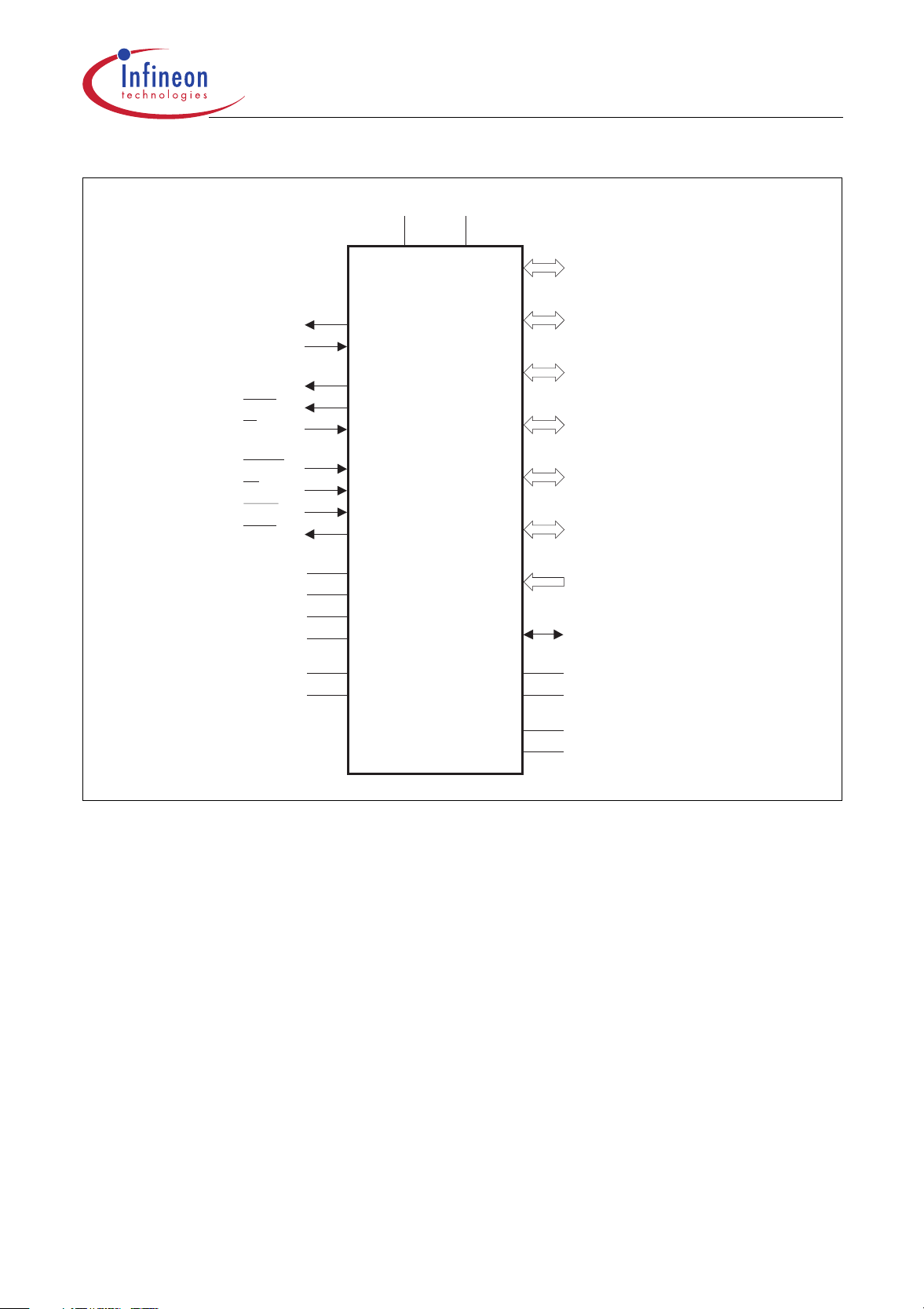
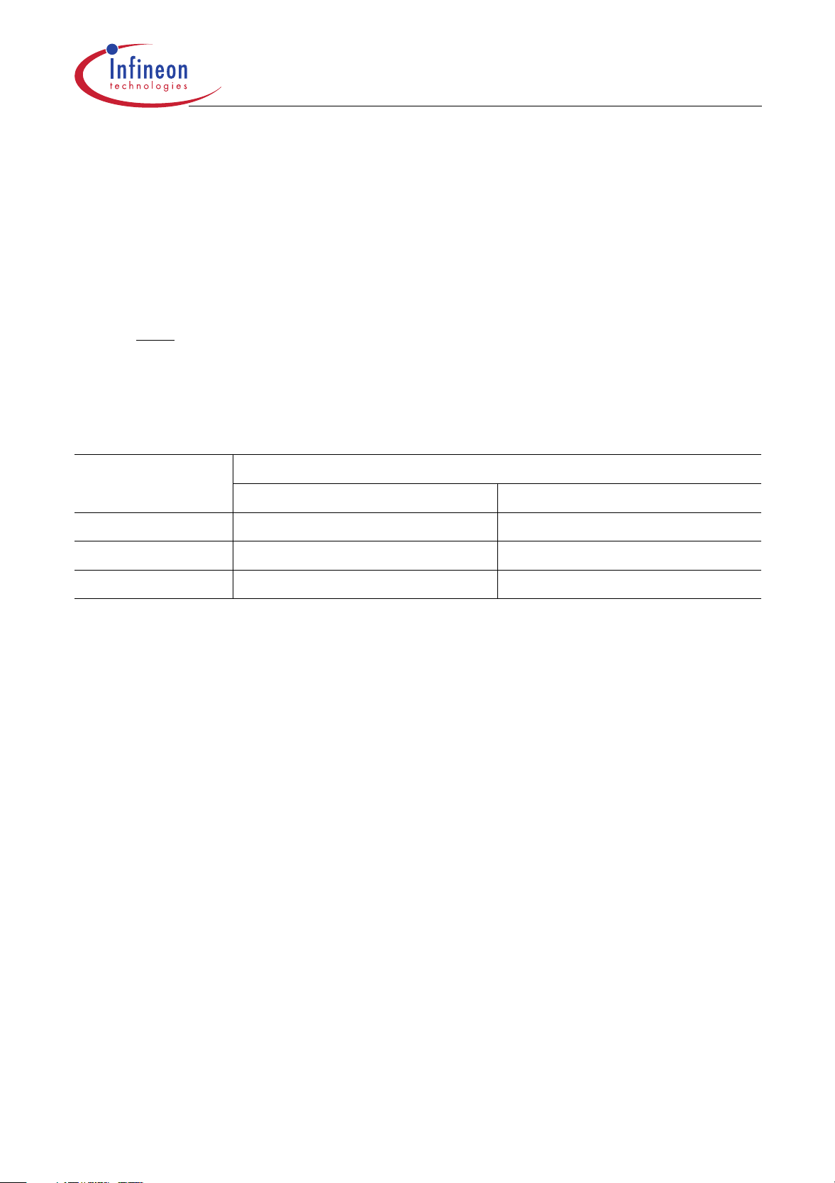
C515C
XTAL1
XTAL2
ALE
PSEN
EA
RESET
PE/SWD
HWPD
CPUR
V
SSE1
V
DDE1
V
SSE2
V
DDE2
V
C515C
V
AREFAGND
Port 0
8 Bit Digital I/O
Port 1
8 Bit Digital I/O
Port 2
8 Bit Digital I/O
Port 3
8 Bit Digital I/O
Port 4
8 Bit Digital I/O
Port 5
8 Bit Digital I/O
Port 6
8 Bit Analog/
Digital Inputs
Port 7
1 Bit Digital I/O
V
SS1
V
DD1
Figure 2 Logic Symbol
V
SSCLK
V
DDCLK
V
SSEXT
V
DDEXT
MCL02714
Data Sheet 4 2003-02
C515C
DDEXT
P0.7/AD7
P5.7
P0.6/AD6
P0.5/AD5
P0.4/AD4
P0.3/AD3
P0.2/AD2
SSEXT
P0.1/AD1
P0.0/AD0EAALE
V
V
PSEN
CPUR
P2.7/A15
P2.6/A14
P2.5/A13
P2.4/A12
P2.3/A11
4142434445464748495051525354555657585960
P5.6
P5.5
P5.4
P5.3
P5.2
P5.1
P5.0
V
DDE2
HWPD
V
SSE2
N.C.
P4.0/ADST
P4.1/SCLK
P4.2/SRI
PE/SWD
P4.3/STO
P4.4/SLS
P4.5/INT8
P4.6/TXDC
P4.7/RXDC
62
63
64
65
66
67
68
69
70
71
72
73
74
75
76
77
78
79
80
12
345
4061
39
38
37
36
35
34
33
32
C515C
31
30
29
28
27
26
25
24
23
22
21
6
7
8
9
10
11
12
13 14 15
16
17
18
19
20
P2.2/A10
P2.1/A9
P2.0/A8
XTAL1
XTAL2
V
SSE1
V
SS1
V
DD1
V
DDE1
P1.0/INT3/CC0
P1.1/INT4/CC1
P1.2/INT5/CC2
P1.3/INT6/CC3
P1.4/INT2
P1.5/T2EX
P1.6/CLKOUT
P1.7/T2
P7.0/INT7
P3.7/RD
P3.6/WR
N.C.
AREF
V
RESET
AGND
V
P6.7/AIN7
P6.5/AIN5
P6.6/AIN6
P6.3/AIN3
P6.4/AIN4
P6.2/AIN2
SSCLK
DDCLK
V
V
P6.0/AIN0
P6.1/AIN1
P3.1/TXD
P3.0/RXD
P3.2/INT0
P3.3/INT1
P3.4/T0
P3.5/T1
MCP02715
Figure 3 C515C Pin Configuration P-MQFP-80-1 (top view)
Data Sheet 5 2003-02
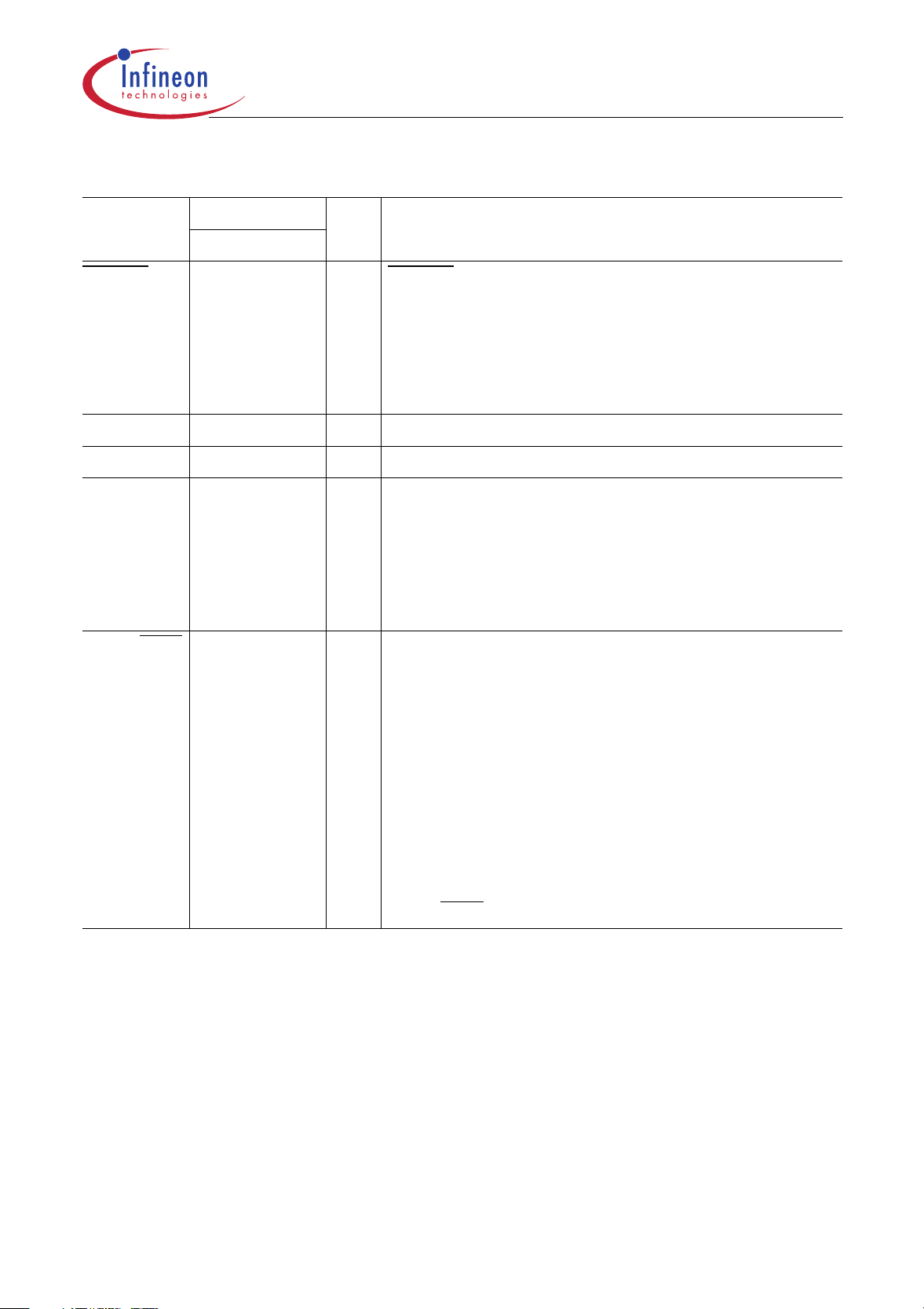
Table 2 Pin Definitions and Functions
Symbol Pin Number I/O
1)
Function
P-MQFP-80-1
C515C
RESET
1IRESET
A low level on this pin for the duration of two
machine cycles while the oscillator is running resets
the C515C. A small internal pullup resistor permits
power-on reset using only a capacitor connected to
V
.
SS
V
AREF
V
AGND
3–Reference voltage for the A/D converter
4–Reference ground for the A/D converter
P6.0-P6.7 12-5 I Port 6
is an 8-bit unidirectional input port to the
A/D converter. Port pins can be used for digital
input, if voltage levels simultaneously meet the
specifications high/low input voltages and for the
eight multiplexed analog inputs.
P7.0 / INT7
23 I/O Port 7
is an 1-bit quasi-bidirectional I/O port with internal
pull-up resistor. When a 1 is written to P7.0 it is
pulled high by an internal pull-up resistor, and in that
state can be used as input. As input, P7.0 being
externally pulled low will source current (
DC characteristics) because of the internal pull-up
resistor. If P7.0 is used as interrupt input, its output
latch must be programmed to a one (1). The
secondary function is assigned to the port 7 pin as
follows:
P7.0 INT7
, Interrupt 7 input
I
, in the
IL
Data Sheet 6 2003-02

Table 2 Pin Definitions and Functions (cont’d)
1)
Symbol Pin Number I/O
Function
P-MQFP-80-1
C515C
P3.0-P3.7 15-22
15
16
17
18
19
20
21
22
I/O Port 3
is an 8-bit quasi-bidirectional I/O port with internal
pullup resistors. Port 3 pins that have 1's written to
them are pulled high by the internal pullup resistors,
and in that state can be used as inputs. As inputs,
port 3 pins being externally pulled low will source
current (
the internal pullup resistors. Port 3 also contains the
interrupt, timer, serial port and external memory
strobe pins that are used by various options. The
output latch corresponding to a secondary function
must be programmed to a one (1) for that function to
operate. The secondary functions are assigned to
the pins of port 3, as follows:
P3.0 RXD Receiver data input (asynch.) or
P3.1 TXD Transmitter data output (asynch.)
P3.2 INT0
P3.3 INT1
P3.4 T0 Timer 0 counter input
P3.5 T1 Timer 1 counter input
P3.6 WR
P3.7 RD
I
, in the DC characteristics) because of
IL
data input/output (synch.) of
serial interface
or clock output (synch.) of serial
interface
External interrupt 0 input / timer 0
gate control input
External interrupt 1 input / timer 1
gate control input
WR control output; latches the
data byte from port 0 into the
external data memory
RD control output; enables the
external data memory
Data Sheet 7 2003-02
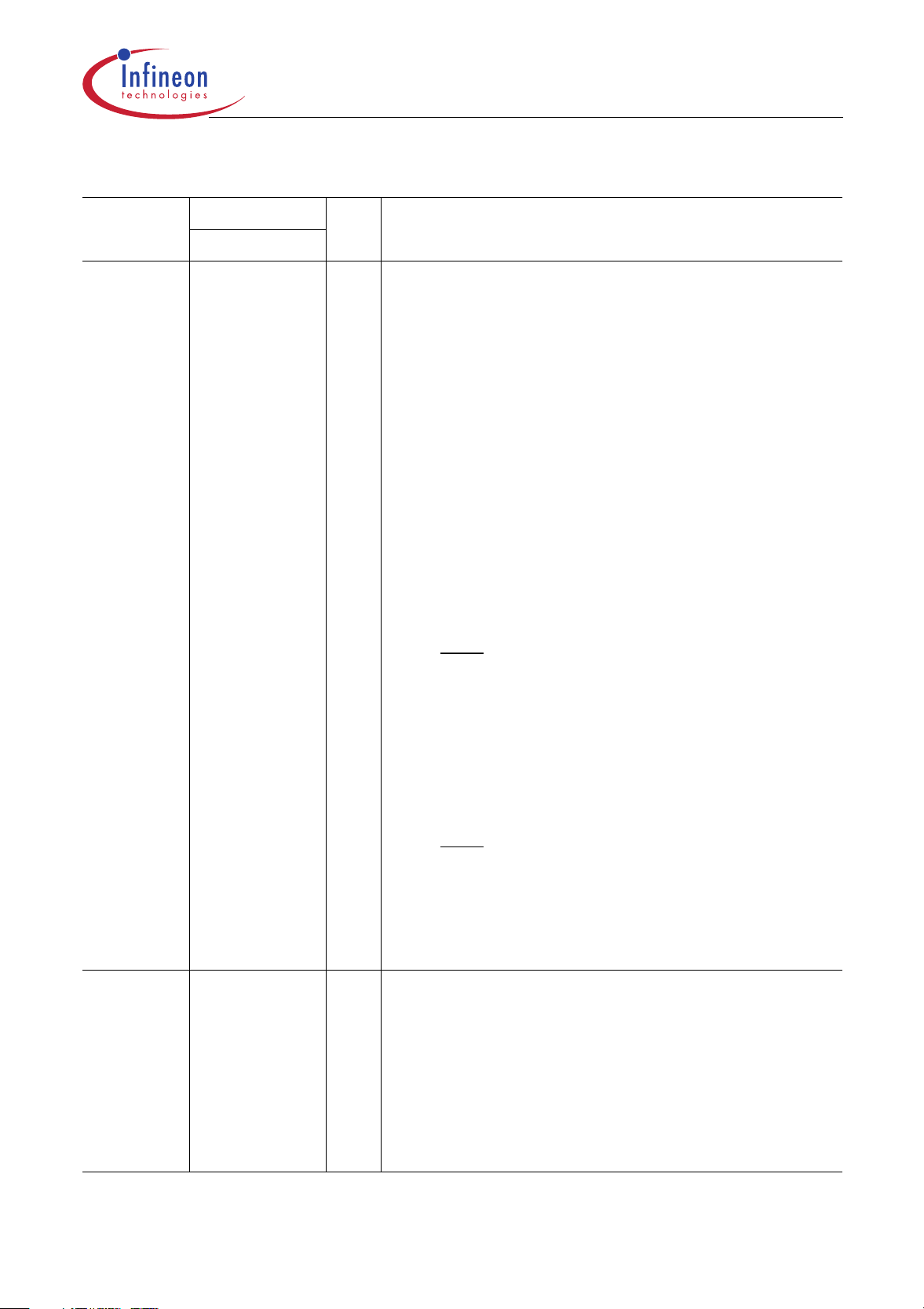
Table 2 Pin Definitions and Functions (cont’d)
Symbol Pin Number I/O
1)
Function
P-MQFP-80-1
C515C
P1.0 - P1.7 31-24
31
30
29
28
27
26
25
24
I/O Port 1
is an 8-bit quasi-bidirectional I/O port with internal
pullup resistors. Port 1 pins that have 1's written to
them are pulled high by the internal pullup resistors,
and in that state can be used as inputs. As inputs,
port 1 pins being externally pulled low will source
current (
the internal pullup resistors. The port is used for the
low-order address byte during program verification.
Port 1 also contains the interrupt, timer, clock,
capture and compare pins that are used by various
options. The output latch corresponding to a
secondary function must be programmed to a one
(1) for that function to operate (except when used for
the compare functions). The secondary functions
are assigned to the port 1 pins as follows:
P1.0 INT3
P1.1 INT4 CC1 Interrupt 4 input / compare 1
P1.2 INT5 CC2 Interrupt 5 input / compare 2
P1.3 INT6 CC3 Interrupt 6 input / compare 3
P1.4 INT2
P1.5 T2EX Timer 2 external reload / trigger
P1.6 CLKOUT System clock output
P1.7 T2 Counter 2 input
I
, in the DC characteristics) because of
IL
CC0 Interrupt 3 input / compare 0
output / capture 0 input
output / capture 1 input
output / capture 2 input
output / capture 3 input
Interrupt 2 input
input
XTAL2 36 I XTAL2
Input to the inverting oscillator amplifier and input to
the internal clock generator circuits.
To drive the device from an external clock source,
XTAL2 should be driven, while XTAL1 is left
unconnected. Minimum and maximum high and low
times as well as rise/fall times specified in the AC
characteristics must be observed.
Data Sheet 8 2003-02

Table 2 Pin Definitions and Functions (cont’d)
1)
Symbol Pin Number I/O
Function
P-MQFP-80-1
XTAL1 37 O XTAL1
Output of the inverting oscillator amplifier.
P2.0-P2.7 38-45 I/O Port 2
is an 8-bit quasi-bidirectional I/O port with internal
pullup resistors. Port 2 pins that have 1's written to
them are pulled high by the internal pullup resistors,
and in that state can be used as inputs. As inputs,
port 2 pins being externally pulled low will source
current (
I
, in the DC characteristics) because of
IL
the internal pullup resistors.
Port 2 emits the high-order address byte during
fetches from external program memory and during
accesses to external data memory that use 16-bit
addresses (MOVX @DPTR). In this application it
uses strong internal pullup resistors when issuing
1's. During accesses to external data memory that
use 8-bit addresses (MOVX @Ri), port 2 issues the
contents of the P2 special function register.
C515C
CPUR
PSEN
46 O CPU Running Condition
This output pin is at low level when the CPU is
running and program fetches or data accesses in
the external data memory area are executed. In idle
mode, hardware and software power down mode,
and with an active RESET
signal CPUR is set to
high level.
CPUR
can be typically used for switching external
memory devices into power saving modes.
47 O The Program Store Enable
output is a control signal that enables the external
program memory to the bus during external fetch
operations. It is activated every six oscillator
periods, except during external data memory
accesses. The signal remains high during internal
program execution.
Data Sheet 9 2003-02

Table 2 Pin Definitions and Functions (cont’d)
1)
Symbol Pin Number I/O
Function
P-MQFP-80-1
ALE 48 O The Address Latch Enable
output is used for latching the address into external
memory during normal operation. It is activated
every six oscillator periods, except during an
external data memory access. ALE can be switched
off when the program is executed internally.
C515C
EA
49 I External Access Enable
When held high, the C515C executes instructions
always from the internal ROM. When held low, the
C515C fetches all instructions from external
program memory.
Note: For the ROM protection version EA
P0.0-P0.7 52-59 I/O Port 0
is an 8-bit open-drain bidirectional I/O port.
Port 0 pins that have 1's written to them float, and in
that state can be used as high-impedance inputs.
Port 0 is also the multiplexed low-order address and
data bus during accesses to external program and
data memory. In this application it uses strong
internal pullup resistors when issuing 1's.
Port 0 also outputs the code bytes during program
verification in the C515C. External pullup resistors
are required during program verification.
pin is
latched during reset.
P5.0-P5.7 67-60 I/O Port 5
is an 8-bit quasi-bidirectional I/O port with internal
pullup resistors. Port 5 pins that have 1's written to
them are pulled high by the internal pullup resistors,
and in that state can be used as inputs. As inputs,
port 5 pins being externally pulled low will source
current (
I
, in the DC characteristics) because of
IL
the internal pullup resistors.
Port 5 can also be switched into a bidirectional
mode, in which CMOS levels are provided. In this
bidirectional mode, each port 5 pin can be
programmed individually as input or output.
Data Sheet 10 2003-02
Table 2 Pin Definitions and Functions (cont’d)
1)
Symbol Pin Number I/O
Function
P-MQFP-80-1
C515C
HWPD
69 I Hardware Power Down
P4.0-P4.7 72-74, 76-80
72
73
74
76
77
78
79
80
A low level on this pin for the duration of one
machine cycle while the oscillator is running resets
the C515C.
A low level for a longer period will force the part to
power down mode with the pins floating.
I/O Port 4
is an 8-bit quasi-bidirectional I/O port with internal
pull-up resistors. Port 4 pins that have 1’s written to
them are pulled high by the internal pull-up resistors,
and in that state can be used as inputs. As inputs,
port 4 pins being externally pulled low will source
current (
the internal pull-up resistors.
P4 also contains the external A/D converter control
pin, the SSC pins, the CAN controller input/output
lines, and the external interrupt 8 input. The output
latch corresponding to a secondary function must
be programmed to a one (1) for that function to
operate. The alternate functions are assigned to
port 4 as follows:
P4.0 ADST
P4.1 SCLK SSC Master Clock Output /
P4.2 SRI SSC Receive Input
P4.3 STO SSC Transmit Output
P4.4 SLS
P4.5 INT8
P4.6 TXDC Transmitter output of the CAN
P4.7 RXDC Receiver input of the CAN controller
I
, in the DC characteristics) because of
IL
External A/D converter start pin
SSC Slave Clock Input
Slave Select Input
External interrupt 8 input
controller
Data Sheet 11 2003-02

Table 2 Pin Definitions and Functions (cont’d)
1)
Symbol Pin Number I/O
Function
P-MQFP-80-1
PE
/SWD 75 I Power saving mode enable / Start watchdog
timer
A low level on this pin allows the software to enter
the power down, idle and slow down mode. In case
the low level is also seen during reset, the watchdog
timer function is off on default.
Use of the software controlled power saving modes
is blocked, when this pin is held on high level. A high
level during reset performs an automatic start of the
watchdog timer immediately after reset. When left
unconnected this pin is pulled high by a weak
internal pull-up resistor.
C515C
V
SSCLK
V
DDCLK
V
DDE1
V
DDE2
V
SSE1
V
SSE2
V
DD1
V
SS1
13 – Ground (0 V) for on-chip oscillator
This pin is used for ground connection of the on-chip
oscillator circuit.
14 – Supply voltage for on-chip oscillator
This pin is used for power supply of the on-chip
oscillator circuit.
32
68
– Supply voltage for I/O ports
These pins are used for power supply of the I/O
ports during normal, idle, and power down mode.
35
70
– Ground (0 V) for I/O ports
These pins are used for ground connections of the
I/O ports during normal, idle, and power down
mode.
33 – Supply voltage for internal logic
This pins is used for the power supply of the internal
logic circuits during normal, idle, and power down
mode.
34 – Ground (0 V) for internal logic
This pin is used for the ground connection of the
internal logic circuits during normal, idle, and power
down mode.
Data Sheet 12 2003-02
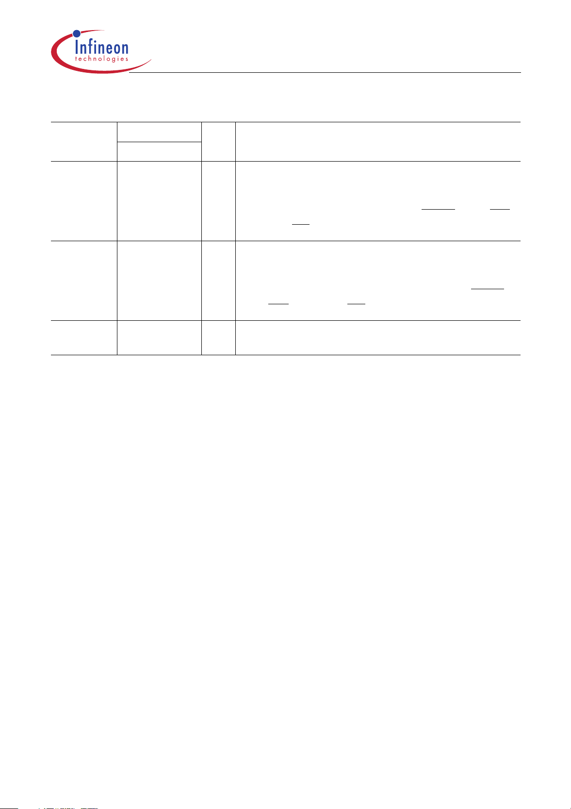
Table 2 Pin Definitions and Functions (cont’d)
Symbol Pin Number I/O
1)
Function
P-MQFP-80-1
C515C
V
DDEXT
50 – Supply voltage for external access pins
This pin is used for power supply of the I/O ports and
control signals which are used during external
accesses (for Port 0, Port 2, ALE, PSEN
V
SSEXT
and P3.7/RD
51 – Ground (0 V) for external access pins
).
This pin is used for the ground connection of the I/O
ports and control signals which are used during
external accesses (for Port 0, Port 2, ALE, PSEN
P3.6/WR
, and P3.7/RD).
N.C. 2, 71 – Not connected
These pins should not be connected.
1)
I = Input; O = Output
, P3.6/WR,
,
Data Sheet 13 2003-02
C515C
XTAL1
XTAL2
ALE
PSEN
EA
CPUR
PE/SWD
HWPD
RESET
Oscillator Watchdog
OSC & Timing
CPU
8 Datapointers
Programmable
Watchdog Timer
Timer 0
Timer 1
Timer 2
Capture
Compare Unit
XRAM
2k x 8 256 x 8
RAM ROM/OTP
64k x 8
Emulation
Support
Logic
Port 0
Port 1
Port 2
Multiple
V
V
/
DD SS
Lines
Port 0
8 Bit Digital I/O
Port 1
8 Bit Digital I/O
Port 2
8 Bit Digital I/O
USART
Baud Rate Generator
SSC (SPI) Interface
Full-CAN
Controller
256 Byte
Reg./Data
Interrupt Unit
V
AREF
V
AGND
A/D Converter
S & H
10 Bit
MUX
Figure 4 Block Diagram of the C515C
Port 3
Port 4
Port 5
Port 6
Port 7
C515C
Port 3
8 Bit Digital I/O
Port 4
8 Bit Digital I/O
Port 5
8 Bit Digital I/O
Port 6
8 Bit Analog/
Digital Inputs
Port 7
1 Bit Digital I/O
MCB03647
Data Sheet 14 2003-02
C515C
CPU
The C515C is efficient both as a controller and as an arithmetic processor. It has
extensive facilities for binary and BCD arithmetic and excels in its bit-handling
capabilities. Efficient use of program memory results from an instruction set consisting
of 44% one-byte, 41% two-byte, and 15% three-byte instructions. With a 6 MHz crystal,
58% of the instructions are executed in 1
PSW
Special Function Register (D0
Bit No. MSB LSB
µs (10 MHz: 600 ns).
) Reset Value: 00
H
H
D7
H
CY AC F0 RS1 RS0 OV F1 PD0
D6
H
D5
H
D4
H
Bit Function
CY Carry Flag
Used by arithmetic instruction.
AC Auxiliary Carry Flag
Used by instructions which execute BCD operations.
F0 General Purpose Flag
RS1
RS0
Register Bank select control bits
These bits are used to select one of the four register banks.
RS1 RS0 Function
0 0 Bank 0 selected, data address 00
0 1 Bank 1 selected, data address 08H-0F
1 0 Bank 2 selected, data address 10H-17
1 1 Bank 3 selected, data address 18H-1F
D3
H
D2
H
D1
H
D0
H
H
PSW
-07
H
H
H
H
H
OV Overflow Flag
Used by arithmetic instruction.
F1 General Purpose Flag
PParity Flag
Set/cleared by hardware after each instruction to indicate an
odd/even number of “one” bits in the accumulator, i.e. even parity.
Data Sheet 15 2003-02
C515C
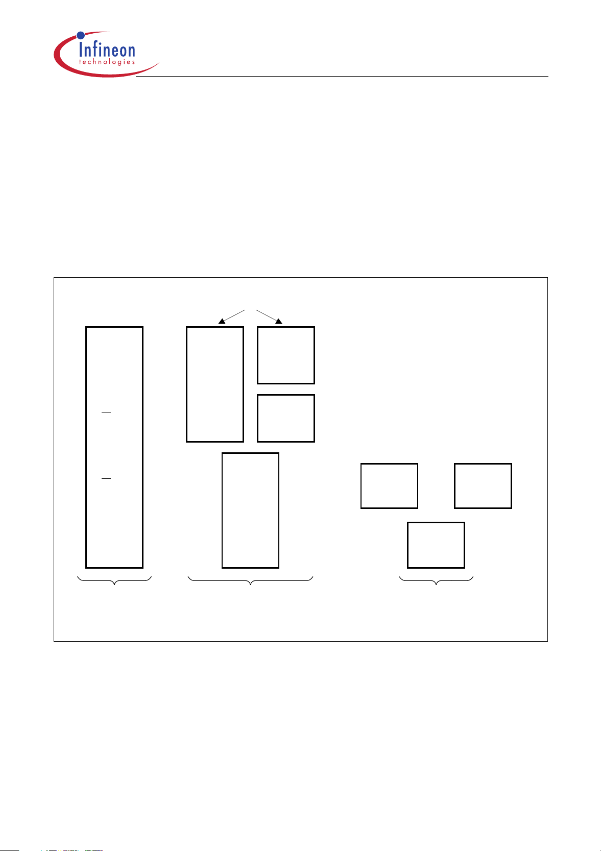
Memory Organization
The C515C CPU manipulates data and operands in the following five address spaces:
• up to 64 Kbytes of internal/external program memory
• up to 64 Kbytes of external data memory
• 256 bytes of internal data memory
• 256 bytes CAN controller registers / data memory
• 2 Kbytes of internal XRAM data memory
• a 128 byte special function register area
Figure 5 illustrates the memory address spaces of the C515C.
Alternatively
FFFF
Internal
(EA = 1)
External
(EA = 0)
0000
"Code Space"
FFFF
F800
F7FF
F700
H
H
H
H
Indirect
Address
Internal
RAM
FF
H
80
H
Internal
RAM
Direct
Address
Special
Function
Register
7F
H
00
H
FF
H
80
H
MCD02717
H
Internal
XRAM
External
Data
Memory
External
H
"Data Space" "Internal Data Space"
(2 KByte)
Int. CAN
Controller
(256 Byte)
F6FF
H
0000
H
Figure 5 C515C Memory Map
Data Sheet 16 2003-02
C515C
Control of XRAM/CAN Controller Access
The XRAM in the C515C is a memory area that is logically located at the upper end of
the external memory space, but is integrated on the chip. Because the XRAM and the
CAN controller is used in the same way as external data memory the same instruction
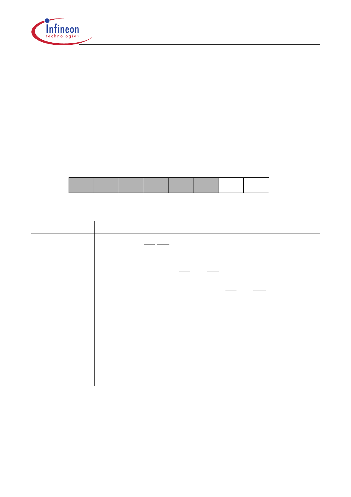
types (MOVX) must be used for accessing the XRAM. Two bits in SFR SYSCON,
XMAP0 and XMAP1, control the accesses to the XRAM and the CAN controller.
SYSCON
Special Function Register (B1
Bit No. MSB LSB
76543210
) C515C-8R Reset Value: X010XX01
H
C515C-8E Reset Value: X010X001
B
B
B1
H
–PMOD
The function of the shaded bits is not described in this section.
EALE RMAP –
CSWO XMAP1
XMAP0
SYSCON
Bit Function
XMAP1 XRAM/CAN controller visible access control
Control bit for RD
/WR signals during XRAM/CAN Controller
accesses. If addresses are outside the XRAM/CAN controller
address range or if XRAM is disabled, this bit has no effect.
XMAP1 = 0: The signals RD
and WR are not activated during
accesses to the XRAM/CAN Controller
XMAP1 = 1: Ports 0, 2 and the signals RD
and WR are activated
during accesses to XRAM/CAN Controller. In this
mode, address and data information during
XRAM/CAN Controller accesses are visible externally.
XMAP0 Global XRAM/CAN controller access enable/disable control
XMAP0 = 0: The access to XRAM and CAN controller is enabled.
XMAP0 = 1: The access to XRAM and CAN controller is disabled
(default after reset). All MOVX accesses are
performed via the external bus. Further, this bit is
hardware protected.
Bit XMAP0 is hardware protected. If it is reset once (XRAM/CAN controller access
enabled) it cannot be set by software. Only a reset operation will set the XMAP0 bit
again.
Data Sheet 17 2003-02

C515C
The XRAM/CAN controller can be accessed by read/write instructions (MOVX A,DPTR,
MOVX @DPTR,A), which use the 16-bit DPTR for indirect addressing. For accessing the
XRAM or CAN controller, the effective address stored in DPTR must be in the range of
F700
The XRAM can be also accessed by read/write instructions (MOVX A,@Ri, MOVX
@Ri,A), which use only an 8-bit address (indirect addressing with registers R0 or R1).
Therefore, a special page register XPAGE which provides the upper address information
(A8-A15) during 8-bit XRAM accesses. The behaviour of Port 0 and P2 during a MOVX
access depends on the control bits XMAP0 and XMAP1 in register SYSCON and on the
state of pin
to FFFFH.
H
EA. Table 3 lists the various operating conditions.
Data Sheet 18 2003-02
C515C
Table 3 Behaviour of P0/P2 and RD
00 10 X1
EA
= 0 MOVX
@DPTR
MOVX
@ Ri
DPTR
<
XRAM/CAN
address range
DPTR
≥
XRAMCAN
address range
XPAGE
<
XRAMCAN
addr. page
range
XPAGE
≥
XRAMCAN
addr. page
range
a) P0/P2→Bus
b) RD
/WR active
c) ext.memory
is used
a) P0/P2
(RD
b) RD
c) XRAM is used
a) P0→Bus
P2
b) RD
c) ext.memory
is used
a) P0
(RD
P2
b) RD
c) XRAM is used
→Bus
/WR-Data)
/WR inactive
→I/O
/WR active
→Bus
/WR-Data)
→I/O
/WR inactive
/WR During MOVX Accesses
XMAP1, XMAP0
a) P0/P2→Bus
b) RD
/WR active
c) ext.memory
is used
a) P0/P2
(RD
b) RD
c) XRAM is used
a) P0→Bus
P2
b) RD
c) ext.memory
is used
a) P0
(RD
P2
b) RD
c) XRAM is used
→Bus
/WR-Data)
/WR active
→I/O
/WR active
→Bus
/WR-Data only)
→I/O
/WR active
a) P0/P2→Bus
b) RD
c) ext.memory
is used
a) P0/P2→Bus
b) RD
c) ext.memory
is used
a) P0→Bus
P2
→I/O
b) RD
c) ext.memory
is used
a) P0→Bus
P2
→I/O
b) RD
c) ext.memory
is used
/WR active
/WR active
/WR active
/WR active
EA
= 1 MOVX
@DPTR
MOVX
@ Ri
DPTR
<
XRAM/CAN
address range
DPTR
≥
XRAMCAN
address range
XPAGE
<
XRAMCAN
addr. page
range
XPAGE
≥
XRAMCAN
addr. page
range
a) P0/P2→Bus
b) RD
/WR active
c) ext.memory
is used
a) P0/P2
b) RD/WR inactive
c) XRAM is used
a) P0→Bus
P2
b) RD
c) ext.memory
is used
a) P2
P0/P2
b) RD
c) XRAM is used
→Ι/0
→I/O
/WR active
→I/O
→I/O
/WR inactive
a) P0/P2→Bus
b) RD
/WR active
c) ext.memory
is used
a) P0/P2
(RD
b) RD
c) XRAM is used
a) P0→Bus
P2
b) RD
c) ext.memory is
used
a) P0
(RD
P2
b) RD
c) XRAM is used
→Bus
/WR-Data)
/WR active
→I/O
/WR active
→Bus
/WR-Data)
→I/O
/WR active
a) P0/P2→Bus
b) RD
/WR active
c) ext.memory
is used
a) P0/P2→Bus
b) RD
/WR active
c) ext.memory
is used
a) P0→Bus
P2
→I/O
b) RD
/WR active
c) ext.memory
is used
a) P0→Bus
P2
→I/O
b) RD
/WR active
c) ext.memory
is used
modes compatible to 8051/C501 family
Data Sheet 19 2003-02
Reset and System Clock
C515C
The reset input is an active low input at pin RESET
internally, the RESET
pin must be held low for at least two machine cycles (12 oscillator
periods) while the oscillator is running. A pullup resistor is internally connected to
. Since the reset is synchronized
V
to
DD
allow a power-up reset with an external capacitor only. An automatic reset can be
V
obtained when
is applied by connecting the RESET pin to VSS via a capacitor.
DD
Figure 6 shows the possible reset circuitries.
b)a)
&
+
RESET
C515C
RESET
C515C
c)
+
RESET
C515C
MCS02721
Figure 6 Reset Circuitries
Figure 7 shows the recommended oscillator circiutries for crystal and external clock
operation.
Data Sheet 20 2003-02
C515C
Crystal/Resonator Oscillator Mode Driving from External Source
C
2 - 10 MHz
C
Crystal Mode :
XTAL1
XTAL2 XTAL2
C = 20 pF ± 10 pF (incl. stray capacitance)
:Resonator Mode
= depends on selected ceramic resonatorC
N.C.
External Oscillator
Signal
XTAL1
MCT02765
Figure 7 Recommended Oscillator Circuitries
Multiple Datapointers
As a functional enhancement to the standard 8051 architecture, the C515C contains
eight 16-bit datapointers instead of only one datapointer. The instruction set uses just
one of these datapointers at a time. The selection of the actual datapointer is done in the
special function register DPSEL. Figure 8 illustrates the datapointer addressing
mechanism.
Datapointer
DPTR 0000
.0.1.2
DPTR7
DPTR0
DPH(83 ) DPL(82 )
HH
External Data Memory
MCD00779
-----
DPSEL(92 )
DPSEL Selected
.2 .1 .0
0 0 1 DPTR 1
0 1 0 DPTR 2
0 1 1 DPTR 3
1 0 0 DPTR 4
1 0 1 DPTR 5
1 1 0 DPTR 6
1 1 1 DPTR 7
H
Figure 8 External Data Memory Addressing using Multiple Datapointers
Data Sheet 21 2003-02
C515C
Enhanced Hooks Emulation Concept
The Enhanced Hooks Emulation Concept of the C500 microcontroller family is a new,
innovative way to control the execution of C500 MCUs and to gain extensive information
on the internal operation of the controllers. Emulation of on-chip ROM based programs
is possible, too.
Each production chip has built-in logic for the support of the Enhanced Hooks Emulation
Concept. Therefore, no costly bond-out chips are necessary for emulation. This also
ensure that emulation and production chips are identical.
The Enhanced Hooks Technology, which requires embedded logic in the C500 allows
the C500 together with an EH-IC to function similar to a bond-out chip. This simplifies the
design and reduces costs of an ICE-system. ICE-systems using an EH-IC and a
compatible C500 are able to emulate all operating modes of the different versions of the
C500 microcontrollers. This includes emulation of ROM, ROM with code rollover and
ROMless modes of operation. It is also able to operate in single step mode and to read
the SFRs after a break.
SYSCON
PCON
TCON
Optional
I/O Ports
ICE-System Interface
to Emulation Hardware
RESET
EA
ALE
PSEN
C500
0
MCU Interface Circuit
Port 3 Port 1
Port
Port
2
Target System Interface
RSYSCON
RPCON
RTCON
Enhanced Hooks
RPort 0RPort 2
EH-IC
TEA TALE TPSEN
MCS03280
Figure 9 Basic C500 MCU Enhanced Hooks Concept Configuration
Port 0, port 2 and some of the control lines of the C500 based MCU are used by
Enhanced Hooks Emulation Concept to control the operation of the device during
emulation and to transfer informations about the program execution and data transfer
between the external emulation hardware (ICE-system) and the C500 MCU.
Data Sheet 22 2003-02
C515C
Special Function Registers
The registers, except the program counter and the four general purpose register banks,
reside in the special function register area. The special function register area consists of
two portions: the standard special function register area and the mapped special function
register area. Two special function registers of the C515C (PCON1 and DIR5) are
located in the mapped special function register area. For accessing the mapped special
function register area, bit RMAP in special function register SYSCON must be set. All
other special function registers are located in the standard special function register area
which is accessed when RMAP is cleared (“0”). As long as bit RMAP is set, mapped
special function register area can be accessed. This bit is not cleared by hardware
automatically. Thus, when non-mapped/mapped registers are to be accessed, the bit
RMAP must be cleared/set by software, respectively each.
SYSCON
Special Function Register (B1
) C515C-8R Reset Value: X010XX01
H
C515C-8E Reset Value: X010X001
B
B
Bit No. MSB LSB
76543210
B1
H
–PMOD
The function of the shaded bits is not described in this section.
EALE RMAP –
CSWO XMAP1
XMAP0
SYSCON
Bit Function
RMAP Special function register map bit
RMAP = 0: The access to the non-mapped (standard) special
function register area is enabled (reset value).
RMAP = 1: The access to the mapped special function register
area is enabled.
The 59 special function registers (SFRs) in the standard and mapped SFR area include
pointers and registers that provide an interface between the CPU and the other on-chip
peripherals. The SFRs of the C515C are listed in Table 4 and Table 5. In Table 4 they
are organized in groups which refer to the functional blocks of the C515C. The CANSFRs are also included in Table 4. Table 5 illustrates the contents of the SFRs in
numeric order of their addresses. Table 6 list the CAN-SFRs in numeric order of their
addresses.
Data Sheet 23 2003-02

C515C
Table 4 Special Function Registers - Functional Block
Block Symbol Name Addr Contents after
Reset
CPU ACC
B
DPH
DPL
DPSEL
PSW
SP
SYSCON
A/DConverter
ADCON0
ADCON1
ADDATH
ADDATL
Interrupt
System
IEN0
IEN1
1)
1)
IEN2
1)
IP0
IP1
TCON
T2CON
SCON
1)
1)
1)
IRCON
XRAM XPAGE
SYSCON
Ports P0
P1
P2
P3
P4
P5
DIR5
P6
P7
SYSCON
Watchdog WDTREL
1)
IEN0
1)
IEN1
1)
IP0
Accumulator
B-Register
Data Pointer, High Byte
Data Pointer, Low Byte
Data Pointer Select Register
Program Status Word Register
Stack Pointer
1)
System Control Register C515C-8R
C515C-8E
1)
A/D Converter Control Register 0
A/D Converter Control Register 1
A/D Converter Data Register High Byte
A/D Converter Data Register Low Byte
Interrupt Enable Register 0
Interrupt Enable Register 1
Interrupt Enable Register 2
Interrupt Priority Register 0
Interrupt Priority Register 1
Timer Control Register
Timer 2 Control Register
Serial Channel Control Register
Interrupt Request Control Register
Page Address Register for Extended
on-chip XRAM and CAN Controller
1)
System Control Register C515C-8R
C515C-8E
Port 0
Port 1
Port 2
Port 3
Port 4
Port 5
Port 5 Direction Register
Port 6, Analog/Digital Input
Port 7
1)
System Control Register C515C-8R
C515C-8E
Watchdog Timer Reload Register
Interrupt Enable Register 0
Interrupt Enable Register 1
Interrupt Priority Register 0
E0
F0
83
82
92
D0
81
B1
B1
D8
DC
D9
DA
A8
B8
9A
A9
B9
88
C8
98
C0
91
B1
B1
80
90
A0
B0
E8
F8
F8
DB
FA
B1
86
A8
B8
A9
H
H
H
H
H
H
H
H
H
H
H
H
H
H
H
H
H
H
H
H
H
H
H
H
H
H
H
H
H
H
H
H
H
H
H
H
2)
2)
2)
2)
H
H
2)
2)
2)
2)
2)
2)
2)
2)
2)
2)
2)
2)
2)4)
H
2)
2)
00
H
00
H
00
H
00
H
XXXXX000
00
H
07
H
X010XX01
X010X001
00
H
0XXXX000
00
H
00XXXXXX
00
H
00
H
XX00X00X
00
H
0X000000
00
H
00
H
00
H
00
H
00
H
X010XX01
X010X001
FF
H
FF
H
FF
H
FF
H
FF
H
FF
H
FF
H
–
XXXXXXX1
X010XX01
X010X001
00
H
00
H
00
H
00
H
3)
B
3)
B
3)
B
3)
B
3)
B
3)
B
3)
B
3)
B
3)
B
3)
B
3)
B
3)
B
Data Sheet 24 2003-02

C515C
Table 4 Special Function Registers - Functional Block (cont’d)
Block Symbol Name Addr Contents after
Reset
Serial
Channel
CAN
Controller
ADCON0
PCON
1)
SBUF
SCON
SRELL
SRELH
CR
SR
IR
BTR0
BTR1
GMS0
GMS1
UGML0
UGML1
LGML0
LGML1
UMLM0
UMLM1
LMLM0
LMLM1
MCR0
MCR1
UAR0
UAR1
LAR0
LAR1
MCFG
DB0n
DB1n
DB2n
DB3n
DB4n
DB5n
DB6n
DB7n
1)
A/D Converter Control Register 0
Power Control Register
Serial Channel Buffer Register
Serial Channel Control Register
Serial Channel Reload Register, low byte
Serial Channel Reload Register, high byte
Control Register
Status Register
Interrupt Register
Bit Timing Register Low
Bit Timing Register High
Global Mask Short Register Low
Global Mask Short Register High
Upper Global Mask Long Register Low
Upper Global Mask Long Register High
Lower Global Mask Long Register Low
Lower Global Mask Long Register High
Upper Mask of Last Message Register
Low
Upper Mask of Last Message Register
High
Lower Mask of Last Message Register
Low
Lower Mask of Last Message Register
High
Message Object Registers:
Message Control Register Low
Message Control Register High
Upper Arbitration Register Low
Upper Arbitration Register High
Lower Arbitration Register Low
Lower Arbitration Register High
Message Configuration Register
Message Data Byte 0
Message Data Byte 1
Message Data Byte 2
Message Data Byte 3
Message Data Byte 4
Message Data Byte 5
Message Data Byte 6
Message Data Byte 7
D8
H
87
H
99
H
98
H
AA
H
BA
H
F700
F701
F702
F704
F705
F706
F707
F708
F709
F70A
F70B
F70C
F70D
F70E
F70F
F7n0
F7n1
F7n2
F7n3
F7n4
F7n5
F7n6
F7n7
F7n8
F7n9
F7nA
F7nB
F7nC
F7nD
F7nE
2)
2)
00
00
XX
00
D9
XXXXXX11
101
H
XX
H
XX
H
UU
H
0UUUUUUU
H
UU
H
UUU11111
H
UU
H
UU
H
UU
H
UUUUU000
H
UU
H
UU
H
UU
H
UUUUU000
H
5)
UU
H
5)
UU
H
5)
UU
H
5)
UU
H
5)
UU
H
5)
UUUUU000
H
5)
UUUUUU00
H
5)
XX
H
5)
XX
H
5)
XX
H
5)
XX
H
5)
XX
H
5)
XX
H
5)
XX
H
5)
XX
H
H
H
3)
H
H
H
H
6)
H
6)
H
6)
H
6)
H
6)
H
6)
H
6)
H
6)
H
6)
H
6)
H
6)
H
6)
H
6)
H
6)
H
6)
H
6)
H
6)
H
6)
H
6)
H
6)
H
6)
H
6)
H
6)
H
3)
B
B
6)
B
6)
B
6)
B
6)
B
6)
B
6)
Data Sheet 25 2003-02

C515C
Table 4 Special Function Registers - Functional Block (cont’d)
Block Symbol Name Addr Contents after
Reset
SSC
Interface
Timer 0/
Timer 1
Compare/
Capture Unit/
Timer 2
Power Save
Modes
SSCCON
STB
SRB
SCF
SCIEN
SSCMOD
TCON
TH0
TH1
TL0
TL1
TMOD
CCEN
CCH1
CCH2
CCH3
CCL1
CCL2
CCL3
CRCH
CRCL
TH2
TL2
T2CON
PCON
1)
PCON1
SSC Control Register
SSC Transmit Buffer
SSC Receive Register
SSC Flag Register
SSC Interrupt Enable Register
SSC Mode Test Register
Timer 0/1 Control Register
Timer 0, High Byte
Timer 1, High Byte
Timer 0, Low Byte
Timer 1, Low Byte
Timer Mode Register
Comp./Capture Enable Reg.
Comp./Capture Reg. 1, High Byte
Comp./Capture Reg. 2, High Byte
Comp./Capture Reg. 3, High Byte
Comp./Capture Reg. 1, Low Byte
Comp./Capture Reg. 2, Low Byte
Comp./Capture Reg. 3, Low Byte
Com./Rel./Capt. Reg. High Byte
Com./Rel./Capt. Reg. Low Byte
Timer 2, High Byte
Timer 2, Low Byte
Timer 2 Control Register
Power Control Register
Power Control Register 1 C515C-8R
C515C-8E
1)
This special function register is listed repeatedly since some bits of it also belong to other functional blocks.
2)
Bit-addressable special function registers
3)
“X” means that the value is undefined and the location is reserved.
4)
This SFR is a mapped SFR. For accessing this SFR, bit PDIR in SFR IP1 must be set.
5)
The notation “n” in the message object address definition defines the number of the related message object.
6)
“X” means that the value is undefined and the location is reserved. “U” means that the value is unchanged by
a reset operation. “U” values are undefined (as “X”) after a power-on reset operation.
7)
SFR is located in the mapped SFR area. For accessing this SFR, bit RMAP in SFR SYSCON must be set.
93
94
95
AB
AC
96
88
8C
8D
8A
8B
89
C1
C3
C5
C7
C2
C4
C6
CB
CA
CD
CC
C8
87
88
88
2)
H
H
H
H
H
H
2)
H
H
H
H
H
H
H
H
H
H
H
H
H
H
H
H
H
2)
H
H
7)
H
7)
H
2)
07
H
3)
XX
H
3)
XX
H
XXXXXX00
XXXXXX00
00
H
00
H
00
H
00
H
00
H
00
H
00
H
00
H
00
H
00
H
00
H
00
H
00
H
00
H
00
H
00
H
00
H
00
H
00
H
00
H
0XXXXXXX
0XX0XXXX
3)
B
3)
B
3)
B
3)
B
Data Sheet 26 2003-02
Table 5 Contents of the SFRs, SFRs in Numeric Order
of their Addresses
C515C
Addr. Register Content
after
1)
Reset
2)
80
81
82
83
86
87
88
88
88
89
8A
8B
8C
8D
90
P0 FF
H
SP 07
H
DPL 00
H
DPH 00
H
WDTREL 00
H
PCON 00
H
2)
TCON 00
H
3)
PCON1
H
3)
PCON1
H
TMOD 00
H
TL0 00
H
TL1 00
H
TH0 00
H
TH1 00
H
2)
P1 FF
H
H
H
H
H
H
H
H
4)
0XXXXXXX
B
5)
0XX0XXXX
B
H
H
H
H
H
H
Bit 7 Bit 6 Bit 5 Bit 4 Bit 3 Bit 2 Bit 1 Bit 0
.7 .6 .5 .4 .3 .2 .1 .0
.7 .6 .5 .4 .3 .2 .1 .0
.7 .6 .5 .4 .3 .2 .1 .0
.7 .6 .5 .4 .3 .2 .1 .0
WDT
.6 .5 .4 .3 .2 .1 .0
PSEL
SMOD PDS IDLS SD GF1 GF0 PDE IDLE
TF1 TR1 TF0 TR0 IE1 IT1 IE0 IT0
EWPD – – – – – – –
EWPD – – WS – – – –
GATE C/T M1 M0 GATE C/T M1 M0
.7 .6 .5 .4 .3 .2 .1 .0
.7 .6 .5 .4 .3 .2 .1 .0
.7 .6 .5 .4 .3 .2 .1 .0
.7 .6 .5 .4 .3 .2 .1 .0
T2 CLK-
T2EX INT2 INT6 INT5 INT4 INT3
OUT
91
92
93
94
95
96
98
99
9A
A0
A8
A9
XPAGE 00
H
DPSEL XXXX-
H
SSCCON 07
H
STB XX
H
SRB XX
H
SSCMOD 00
H
2)
SCON 00
H
SBUF XX
H
IEN2 X00X-
H
2)
P2 FF
H
2)
IEN0 00
H
IP0 00
H
H
X000
H
H
H
H
H
H
X00X
H
H
H
.7 .6 .5 .4 .3 .2 .1 .0
– ––––.2.1 .0
B
SCEN TEN MSTR CPOL CPHA BRS2 BRS1 BRS0
.7 .6 .5 .4 .3 .2 .1 .0
.7 .6 .5 .4 .3 .2 .1 .0
LOOPB TRIO 0 0 0 0 0 LSBSM
SM0 SM1 SM2 REN TB8 RB8 TI RI
.7 .6 .5 .4 .3 .2 .1 .0
– – EX8 EX7 – ESSC ECAN –
B
.7 .6 .5 .4 .3 .2 .1 .0
EAL WDT ET2 ES ET1 EX1 ET0 EX0
OWDS WDTS .5 .4 .3 .2 .1 .0
Data Sheet 27 2003-02

Table 5 Contents of the SFRs, SFRs in Numeric Order
of their Addresses (cont’d)
C515C
Addr. Register Content
after
1)
Reset
AA
AB
AC
B0
B1
B1
B8
B9
BA
C0
C1
SRELL D9
H
SCF XXXX-
H
SCIEN XXXX-
H
2)
P3 FF
H
SYSCON4)X010-
H
SYSCON5)X010-
H
2)
IEN1 00
H
IP1 0X00-
H
SRELH XXXX-
H
2)
IRCON 00
H
CCEN 00
H
H
XX00
XX00
H
XX01
X001
H
0000
XX11
H
H
B
B
B
B
B
B
Bit 7 Bit 6 Bit 5 Bit 4 Bit 3 Bit 2 Bit 1 Bit 0
.7 .6 .5 .4 .3 .2 .1 .0
– ––––– WCOLTC
– ––––– WCENTCEN
RD WR T1 T0 INT1 INT0 TxD RxD
– PMOD EALE RMAP – – XMAP1 XMAP0
– PMOD EALE RMAP – CSWO XMAP1 XMAP0
EXEN2 SWDT EX6 EX5 EX4 EX3 EX2 EADC
PDIR – .5 .4 .3 .2 .1 .0
– ––––– .1 .0
EXF2 TF2 IEX6 IEX5 IEX4 IEX3 IEX2 IADC
COCAH3COCAL3COCAH2COCAL2COCAH1COCAL1COCAH0COCA
L0
C2
C3
C4
C5
C6
C7
C8
CA
CB
CC
CD
CCL1 00
H
CCH1 00
H
CCL2 00
H
CCH2 00
H
CCL3 00
H
CCH3 00
H
2)
T2CON 00
H
CRCL 00
H
CRCH 00
H
TL2 00
H
TH2 00
H
H
H
H
H
H
H
H
H
H
H
H
.7 .6 .5 .4 .3 .2 .1 .0
.7 .6 .5 .4 .3 .2 .1 .0
.7 .6 .5 .4 .3 .2 .1 .0
.7 .6 .5 .4 .3 .2 .1 .0
.7 .6 .5 .4 .3 .2 .1 .0
.7 .6 .5 .4 .3 .2 .1 .0
T2PS I3FR I2FR T2R1 T2R0 T2CM T2I1 T2I0
.7 .6 .5 .4 .3 .2 .1 .0
.7 .6 .5 .4 .3 .2 .1 .0
.7 .6 .5 .4 .3 .2 .1 .0
.7 .6 .5 .4 .3 .2 .1 .0
Data Sheet 28 2003-02

Table 5 Contents of the SFRs, SFRs in Numeric Order
of their Addresses (cont’d)
C515C
Addr. Register Content
Bit 7 Bit 6 Bit 5 Bit 4 Bit 3 Bit 2 Bit 1 Bit 0
after
1)
Reset
2)
D0
D8
D9
DA
DB
DC
E0
E8
F0
F8
F8
FA
FC
FD
FE
1)
2)
3)
4)
5)
6)
7)
8)
9)
PSW 00
H
2)
ADCON0 00
H
ADDATH 00
H
ADDATL 00XX-
H
H
H
H
XXXX
P6 – .7 .6 .5 .4 .3 .2 .1 .0
H
ADCON1 0XXX-
H
X000
2)
ACC 00
H
2)
P4 FF
H
2)
B 00
H
2)
P5 FF
H
2)
H
H
6)
DIR5
P7 XXXX-
FF
H
H
H
H
H
XXX1
7)8)
VR0
H
7)8)
VR1
H
7)8)
VR2
H
C5
95
02
H
H
9)
H
CY AC F0 RS1 RS0 OV F1 P
BD CLK ADEX BSY ADM MX2 MX1 MX0
.9 .8 .7 .6 .5 .4 .3 .2
.1 .0–––– – –
B
ADCL – – – 0 MX2 MX1 MX0
B
.7 .6 .5 .4 .3 .2 .1 .0
RXDC TXDC INT8 SLS STO SRI SCLK ADST
.7 .6 .5 .4 .3 .2 .1 .0
.7 .6 .5 .4 .3 .2 .1 .0
.7 .6 .5 .4 .3 .2 .1 .0
– ––––– – INT7
B
1 1 0001 0 1
1 0 0101 0 1
0 0 0000 1 0
“X” means that the value is undefined and the location is reserved.
Bit-addressable special function registers
SFR is located in the mapped SFR area. For accessing this SFR, bit RMAP in SFR SYSCON must be set.
This SFR is available in the C515C-8R and C515C-L.
This SFR is available in the C515C-8E.
This SFR is a mapped SFR. For accessing this SFR, bit PDIR in SFR IP1 must be set.
This SFR is a mapped SFR. For accessing this SFR, bit RMAP in SFR SYSCON must be set.
These SFRs are read-only registers (C515C-8E only).
The content of this SFR varies with the actual step of the C515C-8E (e.g. 01H for the first step).
Data Sheet 29 2003-02

Table 6 Contents of the CAN Registers in Numeric Order
of their Addresses
C515C
Addr.
n = 1 to F
F700
H
F701
H
F702
H
F704
H
F705
H
F706
H
F707
H
F708
H
F709
H
F70A
H
F70B
H
F70C
H
F70D
H
F70E
H
F70F
H
F7n0
H
F7n1
H
Regis-
1)
ter
H
CR 01
SR XX
IR XX
BTR0 UU
BTR1 0UUU.
GMS0 UU
GMS1 UUU1.
UGML0 UU
UGML1 UU
LGML0 UU
LGML1 UUUU.
UMLM0 UU
UMLM1 UU
LMLM0 UU
LMLM1 UUUU.
MCR0 UU
MCR1 UU
Content
after
2)
Reset
H
H
H
H
UUUU
1111
U000
U000
B
H
B
H
H
H
B
H
H
H
B
H
H
Bit 7 Bit 6 Bit 5 Bit 4 Bit 3 Bit 2 Bit 1 Bit 0
TEST CCE 0 0 EIE SIE IE INIT
BOFF EWRN – RXOK TXOK LEC2 LEC1 LEC0
INTID
SJW BRP
0TSEG2 TSEG1
ID28-21
ID20-18 11111
ID28-21
ID20-13
ID12-5
ID4-0 000
ID28-21
ID20-18 ID17-13
ID12-5
ID4-0 000
MSGVAL TXIE RXIE INTPND
RMTPND TXRQ MSGLST
NEWDAT
CPUUPD
F7n2
F7n3
F7n4
F7n5
F7n6
F7n7
F7n8
F7n9
F7nA
F7nB
H
H
H
H
H
H
H
H
H
H
UAR0 UU
UAR1 UU
LAR0 UU
H
H
H
LAR1 UUUU.
U000
MCFG UUUU.
UU00
DB0n XX
DB1n XX
DB2n XX
DB3n XX
DB4n XX
H
H
H
H
H
ID28-21
ID20-18 ID17-13
ID12-5
ID4-0 000
B
DLC DIR XTD 0 0
B
.7 .6 .5 .4 .3 .2 .1 .0
.7 .6 .5 .4 .3 .2 .1 .0
.7 .6 .5 .4 .3 .2 .1 .0
.7 .6 .5 .4 .3 .2 .1 .0
.7 .6 .5 .4 .3 .2 .1 .0
Data Sheet 30 2003-02

Table 6 Contents of the CAN Registers in Numeric Order
of their Addresses (cont’d)
C515C
Addr.
n = 1 to F
F7nC
H
F7nD
H
F7nE
H
1)
The notation “n” in the address definition defines the number of the related message object.
2)
“X” means that the value is undefined and the location is reserved. “U” means that the value is
Regis-
1)
ter
H
DB5n XX
DB6n XX
DB7n XX
Content
after
2)
Reset
H
H
H
Bit 7 Bit 6 Bit 5 Bit 4 Bit 3 Bit 2 Bit 1 Bit 0
.7 .6 .5 .4 .3 .2 .1 .0
.7 .6 .5 .4 .3 .2 .1 .0
.7 .6 .5 .4 .3 .2 .1 .0
unchanged by a reset operation. “U” values are undefined (as “X”) after a power-on reset operation.
Data Sheet 31 2003-02

C515C
Digital I/O Ports
The C515C allows for digital I/O on 49 lines grouped into 6 bidirectional 8-bit ports and
one 1-bit port. Each port bit consists of a latch, an output driver and an input buffer. Read
and write accesses to the I/O ports P0 through P7 are performed via their corresponding
special function registers P0 to P7. The port structure of port 5 of the C515C is especially
designed to operate either as a quasi-bidirectional port structure, compatible to the
standard 8051-Family, or as a genuine bidirectional port structure. This port operating
mode can be selected by software (setting or clearing the bit PMOD in the SFR
SYSCON).
The output drivers of port 0 and 2 and the input buffers of port 0 are also used for
accessing external memory. In this application, port 0 outputs the low byte of the external
memory address, time-multiplexed with the byte being written or read. Port 2 outputs the
high byte of the external memory address when the address is 16 bits wide. Otherwise,
the port 2 pins continue emitting the P2 SFR contents.
Analog Input Ports
Ports 6 is available as input port only and provides two functions. When used as digital
inputs, the corresponding SFR P6 contains the digital value applied to the port 6 lines.
When used for analog inputs the desired analog channel is selected by a three-bit field
in SFR ADCON0 or SFR ADCON1. Of course, it makes no sense to output a value to
these input-only ports by writing to the SFR P6. This will have no effect.
If a digital value is to be read, the voltage levels are to be held within the input voltage
specifications (
V
IL/VIH
). Since P6 is not bit-addressable, all input lines of P6 are read at
the same time by byte instructions.
Nevertheless, it is possible to use port 6 simultaneously for analog and digital input.
However, care must be taken that all bits of P6 that have an undetermined value caused
by their analog function are masked.
Data Sheet 32 2003-02

C515C
Port Structure Selection of Port 5
After a reset operation of the C515C, the quasi-bidirectional 8051-compatible port
structure is selected. For selection of the bidirectional (CMOS) port 5 structure the bit
PMOD of SFR SYSCON must be set. Because each port 5 pin can be programmed as
an input or an output, additionally, after the selection of the bidirectional mode the
direction register DIR5 of port 5 must be written. This direction register is mapped to the
port 5 register. This means, the port register address is equal to its direction register
address. Figure 10 illustrates the port and direction register configuration.
Int. Bus, Bit 7
Write to IP 1
Instruction sequence for the programming of the direction registers:
ORL IP1, #80H ; Set bit PDIR
D
RQ
Write port x direction register with value YYH;#OYYHDIRx,MOV
Q
PDIR
Delay:
2.5 Machine Cycles
Figure 10 Port Register, Direction Register
Enable
Enable
Write to Port
Port Register
Direction Register
Read Port
Internal
Bus
MCS02649
Data Sheet 33 2003-02
C515C
Timer / Counter 0 and 1
Timer / Counter 0 and 1 can be used in four operating modes as listed in Table 7:
Table 7 Timer/Counter 0 and 1 Operating Modes
Mode Description TMOD Timer/Counter Input Clock
M1 M0 internal external (max)
f
0 8-bit timer/counter with a
00
divide-by-32 prescaler
1 16-bit timer/counter 0 1
/6 × 32 f
OSC
f
/6 f
OSC
OSC
OSC
/12 × 32
/12
2 8-bit timer/counter with 8-bit
10
autoreload
3 Timer/counter 0 used as
11
one 8-bit timer/counter and
one 8-bit timer / Timer 1
stops
In the “timer” function (C/
Therefore the count rate is
T = ‘0’) the register is incremented every machine cycle.
f
/6.
OSC
In the “counter” function the register is incremented in response to a 1-to-0 transition at
its corresponding external input pin (P3.4/T0, P3.5/T1). Since it takes two machine
f
cycles to detect a falling edge the max. count rate is
INT1 (P3.2, P3.3) can be programmed to function as a gate to facilitate pulse width
/12. External inputs INT0 and
OSC
measurements. Figure 11 illustrates the input clock logic.
P3.4/T0
P3.5/T1
OSC
÷
6
C/T = 0
C/T = 1
Control
f
/6
OSC
Timer 0/1
Input Clock
Gate
(TMOD)
P3.2/INT0
P3.3/INT1
=1
TR0
TR1
_
<
1
&
MCS03117
Figure 11 Timer/Counter 0 and 1 Input Clock Logic
Data Sheet 34 2003-02

C515C
Timer / Counter 2 with Compare/Capture/Reload
The timer 2 of the C515C provides additional compare/capture/reload features, which
allow the selection of the following operating modes:
• Compare: up to 4 PWM signals with 16-bit/600 ns resolution
• Capture: up to 4 high speed capture inputs with 600 ns resolution
• Reload: modulation of timer 2 cycle time
The block diagram in Figure 12 shows the general configuration of timer 2 with the
additional compare/capture/reload registers. The I/O pins which can used for timer 2
control are located as multifunctional port functions at port 1.
P1.5/
T2EX
P1.7/
T2
OSC
Sync.
T2I0
T2I1
Sync.
&
÷6
f
OSC
÷12
T2PS
Bit16 16 Bit 16 Bit 16 Bit
Comparator
Comparator
Comparator
EXEN2
Reload
EXF2
Reload
Timer 2
TH2TL2
Compare
Comparator
Capture
_
<
1
TF2
Input/
Output
Control
Interrupt
Request
P1.0/
INT3/
CC0
P1.1/
INT4/
CC1
P1.2/
INT5/
CC2
P1.2/
INT6/
CCL3/CCH3
CCL2/CCH2
CCL1/CCH1
CRCL/CRCH
CC3
MCB02730
Figure 12 Timer 2 Block Diagram
Data Sheet 35 2003-02

C515C
Timer 2 Operating Modes
The timer 2, which is a 16-bit-wide register, can operate as timer, event counter, or gated
timer. A roll-over of the count value in TL2/TH2 from all 1’s to all 0’s sets the timer
overflow flag TF2 in SFR IRCON, which can generate an interrupt. The bits in register
T2CON are used to control the timer 2 operation.
Timer Mode: In timer function, the count rate is derived from the oscillator frequency. A
prescaler offers the possibility of selecting a count rate of 1/6 or 1/12 of the oscillator
frequency.
Gated Timer Mode: In gated timer function, the external input pin T2 (P1.7) functions as
a gate to the input of timer 2. If T2 is high, the internal clock input is gated to the timer.
T2 = 0 stops the counting procedure. This facilitates pulse width measurements. The
external gate signal is sampled once every machine cycle.
Event Counter Mode: In the event counter function. the timer 2 is incremented in
response to a 1-to-0 transition at its corresponding external input pin T2 (P1.7). In this
function, the external input is sampled every machine cycle. Since it takes two machine
cycles (12 oscillator periods) to recognize a 1-to-0 transition, the maximum count rate is
1/12 of the oscillator frequency. There are no restrictions on the duty cycle of the external
input signal, but to ensure that a given level is sampled at least once before it changes,
it must be held for at least one full machine cycle.
Reload of Timer 2: Two reload modes are selectable:
In mode 0, when timer 2 rolls over from all 1’s to all 0’s, it not only sets TF2 but also
causes the timer 2 registers to be loaded with the 16-bit value in the CRC register, which
is preset by software.
In mode 1, a 16-bit reload from the CRC register is caused by a negative transition at the
corresponding input pin P1.5/T2EX. This transition will also set flag EXF2 if bit EXEN2
in SFR IEN1 has been set.
Data Sheet 36 2003-02

C515C
Timer 2 Compare Modes
The compare function of a timer/register combination operates as follows: the 16-bit
value stored in a compare or compare/capture register is compared with the contents of
the timer register; if the count value in the timer register matches the stored value, an
appropriate output signal is generated at a corresponding port pin and an interrupt can
be generated.
Compare Mode 0
In compare mode 0, upon matching the timer and compare register contents, the output
signal changes from low to high. lt goes back to a low level on timer overflow. As long as
compare mode 0 is enabled, the appropriate output pin is controlled by the timer circuit
only and writing to the port will have no effect. Figure 13 shows a functional diagram of
a port circuit when used in compare mode 0. The port latch is directly controlled by the
timer overflow and compare match signals. The input line from the internal bus and the
write-to-latch line of the port latch are disconnected when compare mode 0 is enabled.
Port Circuit
Compare Register
Circuit
Compare Reg.
16 Bit
Comparator
Bit16
Timer Register
Timer Circuit
Compare
Match
Timer
Overflow
Internal
Bus
Write to
Latch
Figure 13 Port Latch in Compare Mode 0
S
D
Latch
CLK
R
Read Latch
Q
Port
Q
Read Pin
V
DD
Port
Pin
MCS02661
Data Sheet 37 2003-02
C515C
Compare Mode 1
If compare mode 1 is enabled and the software writes to the appropriate output latch at
the port, the new value will not appear at the output pin until the next compare match
occurs. Thus, it can be choosen whether the output signal has to make a new transition
(1-to-0 or 0-to-1, depending on the actual pin-level) or should keep its old value at the
time when the timer value matches the stored compare value.
In compare mode 1 (see Figure 14) the port circuit consists of two separate latches. One
latch (which acts as a “shadow latch”) can be written under software control, but its value
will only be transferred to the port latch (and thus to the port pin) when a compare match
occurs.
Port Circuit
Read Latch
Compare Register
Circuit
Compare Reg.
16 Bit
Comparator
16 Bit
Timer Register
Timer Circuit
Compare
Match
Internal
Bus
Write to
Latch
D
Shadow
Latch
CLK
Q
Figure 14 Compare Function in Compare Mode 1
D
Port
Latch
Read Pin
Q
QCLK
V
DD
Port
Pin
MCS02662
Data Sheet 38 2003-02
C515C
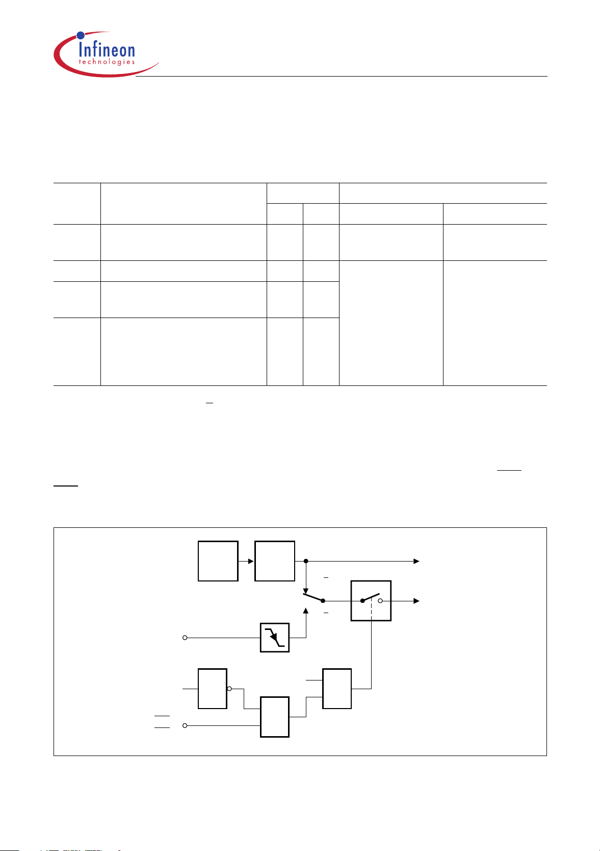
Serial Interface (USART)
The serial port is full duplex and can operate in four modes (one synchronous mode,
three asynchronous modes) as illustrated in Table 8.
Table 8 USART Operating Modes
SCON Description
Mode
SM0 SM1
000Shift register mode, fixed baud rate
Serial data enters and exits through R
the shift clock; 8-bit are transmitted/received (LSB first)
1018-bit UART, variable baud rate
10 bits are transmitted (through T
R
×D)
×D; T×D outputs
×D) or received (at
2109-bit UART, fixed baud rate
11 bits are transmitted (through T
×D)
R
×D) or received (at
3119-bit UART, variable baud rate
Like mode 2
For clarification some terms regarding the difference between “baud rate clock” and
“baud rate” should be mentioned. In the asynchronous modes the serial interfaces
require a clock rate which is 16 times the baud rate for internal synchronization.
Therefore, the baud rate generators/timers have to provide a “baud rate clock” (output
signal in Figure 15 to the serial interface which - there divided by 16 - results in the
actual “baud rate”. Further, the abbreviation
f
refers to the oscillator frequency
OSC
(crystal or external clock operation).
The variable baud rates for modes 1 and 3 of the serial interface can be derived either
from timer 1 or from a dedicated baud rate generator (see Figure 15).
Data Sheet 39 2003-02

Timer 1
Overflow
f
OSC
Baud
Rate
Generator
(SRELH
SRELL)
6÷÷
ADCON0.7
(BD)
0
1
Mode 2
Mode 0
Mode 1
Mode 3
SCON.7
SCON.6
(SM0/
SM1)
Only one mode
can be selected
C515C
PCON.7
2
(SMOD)
0
1
Baud
Rate
Clock
Note: The switch configuration shows the reset state.
MCS02733
Figure 15 Block Diagram of Baud Rate Generation for the Serial Interface
Table 9 below lists the values/formulas for the baud rate calculation of the serial
interface with its dependencies of the control bits BD and SMOD.
Table 9 Serial Interface - Baud Rate Dependencies
Serial Interface
Operating Modes
Active Control
Bits
Baud Rate Calculation
BD SMOD
Mode 0 (Shift
––
f
OSC
/ 6
Register)
Mode 1 (8-bit UART)
Mode 3 (9-bit UART)
0 X Controlled by timer 1 overflow:
SMOD
(2
× timer 1 overflow rate) / 32
1 X Controlled by baud rate generator
(2
(32
SMOD
× f
OSC
) /
× baud rate generator overflow rate)
f
Mode 2 (9-bit UART) – 0
1
Data Sheet 40 2003-02
OSC
f
OSC
/ 32
/ 16

C515C
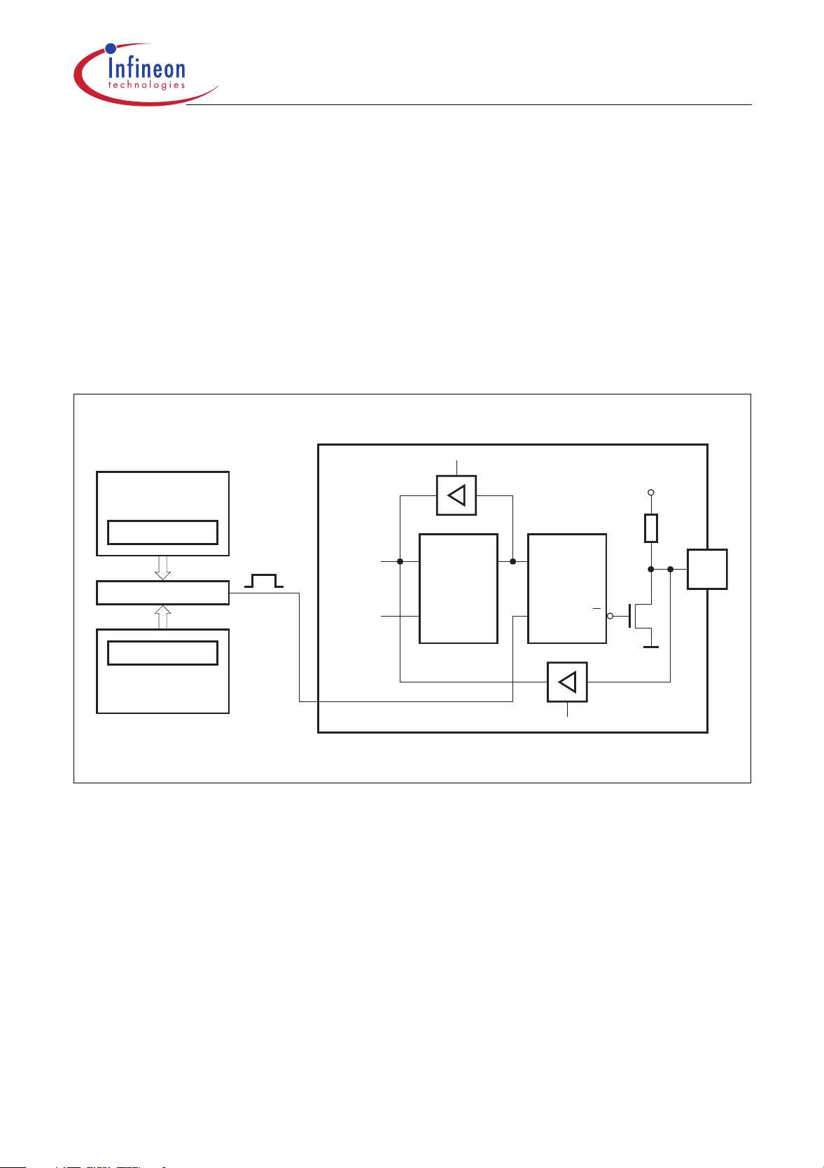
SSC Interface
The C515C microcontroller provides a Synchronous Serial Channel unit, the SSC. This
interface is compatible to the popular SPI serial bus interface. Figure 16 shows the block
diagram of the SSC. The central element of the SSC is an 8-bit shift register. The input
and the output of this shift register are each connected via a control logic to the pin P4.2
/ SRI (SSC Receiver In) and P4.3 / STO (SSC Transmitter Out). This shift register can
be written to (SFR STB) and can be read through the Receive Buffer Register SRB.
f
OSC
Clock Divider
Clock Selection
Receive Buffer Register
Interrupt
SCIEN
Int. Enable Reg.
SSCCON SCF
Control Register Status Register
Control Logic
Shift Register
SRB
STB
Pin
Control
Logic
Internal Bus
P4.1/SCLK
P4.2/SRI
P4.3/STO
P4.4/SLS
MCB02735
Figure 16 SSC Block Diagram
The SSC has implemented a clock control circuit, which can generate the clock via a
baud rate generator in the master mode, or receive the transfer clock in the slave mode.
The clock signal is fully programmable for clock polarity and phase. The pin used for the
clock signal is P4.1 / SCLK. When operating in slave mode, a slave select input is
provided which enables the SSC interface and also will control the transmitter output.
The pin used for this is P4.4 / SLS
.
The SSC control block is responsible for controlling the different modes and operation of
the SSC, checking the status, and generating the respective status and interrupt signals.
Data Sheet 41 2003-02

C515C
CAN Controller
The on-chip CAN controller is the functional heart which provides all resources that are
required to run the standard CAN protocol (11-bit identifiers) as well as the extended
CAN protocol (29-bit identifiers). It provides a sophisticated object layer to relieve the
CPU of as much overhead as possible when controlling many different message objects
(up to 15). This includes bus arbitration, resending of garbled messages, error handling,
interrupt generation, etc. In order to implement the physical layer, external components
have to be connected to the C515C.
The internal bus interface connects the on-chip CAN controller to the internal bus of the
microcontroller. The registers and data locations of the CAN interface are mapped to a
specific 256 bytes wide address range of the external data memory area (F700
F7FF
) and can be accessed using MOVX instructions. Figure 17 shows a block
H
diagram of the on-chip CAN controller.
H
to
Data Sheet 42 2003-02
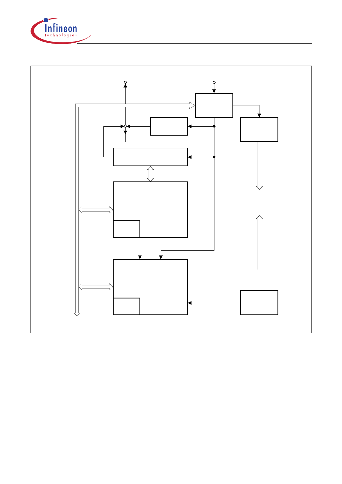
C515C
TXDC RXDC
Messages
Handlers
BTL-Configuration
TX/RX Shift Register
Intelligent
Memory
Interrupt
Register
CRC
Gen./Check
Messages
Bit
Timing
Logic
Timing
Generator
Clocks
(to all)
Control
Status +
Control
Status
Register
to internal Bus
Bit
Stream
Processor
Error
Management
Logic
MCB02736
Figure 17 CAN Controller Block Diagram
The TX/RX Shift Register holds the destuffed bit stream from the bus line to allow the
parallel access to the whole data or remote frame for the acceptance match test and the
parallel transfer of the frame to and from the Intelligent Memory.
The Bit Stream Processor (BSP) is a sequencer controlling the sequential data stream
between the TX/RX Shift Register, the CRC Register, and the bus line. The BSP also
controls the EML and the parallel data stream between the TX/RX Shift Register and the
Intelligent Memory such that the processes of reception, arbitration, transmission, and
error signalling are performed according to the CAN protocol. Note that the automatic
retransmission of messages which have been corrupted by noise or other external error
conditions on the bus line is handled by the BSP.
Data Sheet 43 2003-02

C515C
The Cyclic Redundancy Check Register (CRC) generates the Cyclic Redundancy
Check code to be transmitted after the data bytes and checks the CRC code of incoming
messages. This is done by dividing the data stream by the code generator polynomial.
The Error Management Logic (EML) is responsible for the fault confinement of the
CAN device. Its counters, the Receive Error Counter and the Transmit Error Counter, are
incremented and decremented by commands from the Bit Stream Processor. According
to the values of the error counters, the CAN controller is set into the states error active,
error passive and busoff.
The Bit Timing Logic (BTL) monitors the busline input RXDC and handles the busline
related bit timing according to the CAN protocol. The BTL synchronizes on a recessive
to dominant busline transition at Start of Frame (hard synchronization) and on any further
recessive to dominant busline transition, if the CAN controller itself does not transmit a
dominant bit (resynchronization). The BTL also provides programmable time segments
to compensate for the propagation delay time and for phase shifts and to define the
position of the Sample Point in the bit time. The programming of the BTL depends on the
baudrate and on external physical delay times.
The Intelligent Memory (CAM/RAM array) provides storage for up to 15 message
objects of maximum 8 data bytes length. Each of these objects has a unique identifier
and its own set of control and status bits. After the initial configuration, the Intelligent
Memory can handle the reception and transmission of data without further CPU actions.
Switch-off Capability of the CAN Controller (C515C-8E only)
For power consumption reasons, the on-chip CAN controller in the C515C-8E can be
switched off by setting bit CSWO (bit 2) in SFR SYSCON. When the CAN controller is
switched off its clock signal is turned off and the operation of the CAN controller is
stopped. This switch-off state of the CAN controller is equal to its state in software power
down mode. After clearing bit CSWO again the CAN controller has to be reconfigured.
Data Sheet 44 2003-02

C515C
10-Bit A/D Converter
The C515C includes a high performance / high speed 10-bit A/D-Converter (ADC) with
8 analog input channels. It operates with a successive approximation technique and
uses self calibration mechanisms for reduction and compensation of offset and linearity
errors. The A/D converter provides the following features:
• 8 multiplexed input channels (port 6), which can also be used as digital inputs
• 10-bit resolution
• Single or continuous conversion mode
• Internal or external start-of-conversion trigger capability
• Interrupt request generation after each conversion
• Using successive approximation conversion technique via a capacitor array
• Built-in hidden calibration of offset and linearity errors
The main functional blocks of the A/D converter are shown in Figure 19.
The A/D converter uses basically two clock signals for operation: the input clock
(= 1/tIN) and the conversion clock f
the C515C system clock
f
equal to
. The conversion clock is limited to a maximum frequency of 2 MHz and
OSC
therefore must be adapted to
f
which is applied at the XTAL pins. The input clock fIN is
OSC
f
OSC
ADC
(= 1/t
). These clock signals are derived from
ADC
by programming the conversion clock prescaler. The
f
IN
table in Figure 18 shows the prescaler ratios and the resulting A/D conversion times
which must be selected for typical system clock rates.
Data Sheet 45 2003-02

C515C
ADCL
f
OSC
48÷
MUX
÷
Clock Prescaler
Conversion Clock f
Input ClockINf
ADC
A/D
Converter
_
<
Conditions: f
ADC max
MCU System
2 MHz fIN= f
ADCL Conversion
Clock Rate
(
f
)
OSC
2 MHz 0 .5
4 MHz 0 1
6 MHz 0 1.5
8 MHz 0 2
10 MHz 1 1.25
Figure 18 A/D Converter Clock Selection
=
OSC
Clock
f
[MHz]
ADC
1
CLP
MCS02748
Data Sheet 46 2003-02

C515C
Internal
IEN1 (B8 )
EXEN2 EX6 EX5
H
SWDT
EX3EX4 EX2 EADC
Bus
Port 6
f
OSC
V
AREF
V
AGND
IRCON (C0 )
EXF2
P6 (DB )
P6.7
ADCON1 (DC )
ADCL
ADCON0 (D8 )
BD
Conversion
Clock
Prescaler
H
TF2
IEX6
H
P6.5
P6.6
H
--
H
ADEXCLK
MUX
IEX5
P6.4
-
BSY
S & H
Conversion
Clock
Input
Clock
IEX4
-
ADM
f
f
ADC
IN
IEX3
P6.2P6.3
MX2
MX2
Single/
Continuous
Mode
IADC
IEX2
P6.1
P6.0
MX0
MX1
MX0
MX1
A/D
Converter
ADDATH
(D9 )
.2
.3
.4
.5
.6
.7
.8
MSB
ADDATL
(DA )
HH
-
-
-
-
-
-
LSB
.1
P4.0/ADST
Write to
ADDATL
Start of
Conversion
Internal
Bus
Shaded bit locations are not used in ADC-functions.
MCB02747
Figure 19 A/D Converter Block Diagram
Data Sheet 47 2003-02

C515C
Interrupt System
The C515C provides 17 interrupt sources with four priority levels. Seven interrupts can
be generated by the on-chip peripherals (timer 0, timer 1, timer 2, serial interface,
A/D converter, SSC interface, CAN controller), and ten interrupts may be triggered
externally (P1.5/T2EX, P3.2/INT0, P3.3/INT1, P1.4/INT2, P1.0/INT3
P1.2/INT5, P1.3/INT6, P7.0/INT7
, P4.5/INT8). The wake-up from power-down mode
interrupt has a special functionality which allows to exit from the software power-down
mode by a short low pulse at pin P3.2/INT0
.
In the C515C the 17 interrupt sources are combined to six groups of two or three interrupt
sources. Each interrupt group can be programmed to one of the four interrupt priority
levels. Figure 20 to Figure 22 give a general overview of the interrupt sources and
illustrate the interrupt request and control flags.
, P1.1/INT4,
Data Sheet 48 2003-02
C515C
Highest
P3.2/
INT0
IT0
TCON.0
IE0
TCON.1
EX0
IEN0.0
0003
H
Priority Level
Lowest
Priority Level
A/D Converter
IRCON.0
Timer 0
Overflow
Status
SIE
CR.2
Error
EIE
CR.3
Message
Transmit
CAN Controller Interrupt Sources
Message
Receive
TXIE
MCR0.3/2
RXIE
MCR0.5/4
_
_
<
1
<
1
TCON.5
IADC
TF0
CR.1
see Note
INTPND
MCR0.0/1
EADC
IEN1.0
ET0
IEN0.1
ECANIE
IEN2.1
0043
000B
008B
H
IP1.0 IP0.0
H
H
Polling Sequence
P1.4/
INT2
I2FR
T2CON.5
Bit addressable
Request Flag is
cleared by hardware
Note: Each of the 15 CAN controller message objects provides the bits/flags in the shaded area.
IEX2
IRCON.1
EX2
IEN1.1
004B
H
EAL
IEN0.7
IP1.1 IP0.1
MCS02752
Figure 20 Interrupt Request Sources (Part 1)
Data Sheet 49 2003-02

P3.3/
INT1
SSC
Inerface
IT1
TCON.2
WCOL
SCF.1
TC
SCF.0
WCEN
SCIEN.1
TCEN
SCIEN.0
IE1
TCON.3
_
<
1
EX1
IEN0.2
ESSC
IEN2.2
0013
0093
C515C
Highest
Priority Level
H
Lowest
Priority Level
H
P1.0/
INT3/
CC0
Timer 1
Overflow
P1.1/
INT4/
CC1
IEX3
I3FR EX3
T2CON.6
Bit addressable
Request Flag is
cleared by hardware
IRCON.2
TF1
TCON.7
IEX4
IRCON.3
IEN1.2
ET1
IEN0.3
EX4
IEN1.3
0053
H
001B
H
005B
H
EAL
IEN0.7
IP1.2
IP1.3 IP0.3
IP0.2
Polling Sequence
MCS02753
Figure 21 Interrupt Request Sources (Part 2)
Data Sheet 50 2003-02

C515C
USART
P7.0/
INT7
P1.2/
INT5/
CC2
Timer 2
Overflow
P1.5/
T2EX
P4.5/
INT8
EXEN2
IEN1.7
RI
SCON.0
TI
SCON.1
TF2
IRCON.6
EXF2
IRCON.7
_
<
1
IEX5
IRCON.4
_
<
1
ES
IEN0.4
EX7
IEN2.4
EX5
IEN1.4
ET2
IEN0.5
EX8
IEN2.5
0023
00A3
0063
002B
00AB
Highest
Priority Level
H
Lowest
Priority Level
H
H
IP1.4
H
H
IP0.4
Polling Sequence
P1.3/
INT6/
CC3
Bit addressable
Request Flag is
cleared by hardware
IEX6
IRCON.5
EX6
IEN1.5
006B
H
EAL
IEN0.7
IP1.5 IP0.5
MCS02754
Figure 22 Interrupt Request Sources (Part 3)
Data Sheet 51 2003-02

Table 10 Interrupt Source and Vectors
C515C
Interrupt Source Interrupt Vector
Address
External Interrupt 0 0003
Timer 0 Overflow 000B
External Interrupt 1 0013
Timer 1 Overflow 001B
Serial Channel 0023
Timer 2 Overflow / Ext. Reload 002B
A/D Converter 0043
External Interrupt 2 004B
External Interrupt 3 0053
External Interrupt 4 005B
External Interrupt 5 0063
External Interrupt 6 006B
Wake-up from power-down
007B
H
H
H
H
H
H
H
H
H
H
H
H
H
mode
Interrupt Request Flags
IE0
TF0
IE1
TF1
RI / TI
TF2 / EXF2
IADC
IEX2
IEX3
IEX4
IEX5
IEX6
–
CAN controller 008B
External Interrupt 7 00A3
External Interrupt 8 00AB
SSC interface 0093
H
H
H
H
–
–
–
TC / WCOL
Data Sheet 52 2003-02
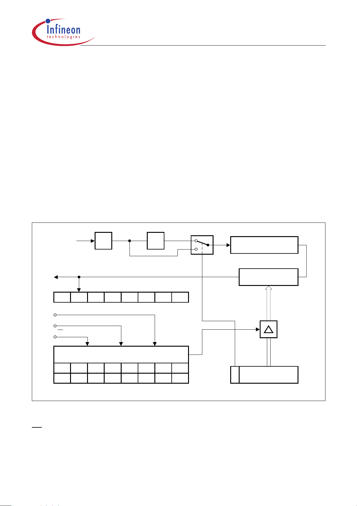
C515C
Fail Save Mechanisms
The C515C offers two on-chip peripherals which monitor the program flow and ensure
an automatic “fail-safe” reaction for cases where the controller’s hardware fails or the
software hangs up:
• A programmable watchdog timer (WDT) with variable time-out period from
512 microseconds up to approx. 1.1 seconds at 6 MHz.
• An oscillator watchdog (OWD) which monitors the on-chip oscillator and forces the
microcontroller into reset state in case the on-chip oscillator fails; it also provides the
clock for a fast internal reset after power-on.
Programmable Watchdog Timer
The watchdog timer in the C515C is a 15-bit timer, which is incremented by a count rate
of
f
/12 up to f
OSC
upper 7 bit of the watchdog timer can be written. Figure 23 shows the block diagram of
the watchdog timer unit.
/192. For programming of the watchdog timer overflow rate, the
OSC
/6
f ÷2
OSC
WDT Reset Request
-------WDTS
External HW Reset
External HW Power-Down
PE/SWD
Control Logic
-
WDT
SWDT -
-
-
-
07
÷16
14 8
IP0 (A9 )
H
WDTPSEL
6
-
-
-
--
IEN0 (A8 )
-
-
-
-
IEN1 (B8 )
H
H
WDTL
WDTH
WDTREL (86 )
H
MCB02755
07
Figure 23 Block Diagram of the Programmable Watchdog Timer
The watchdog timer can be started by software (bit SWDT) or by hardware through pin
PE
/SWD, but it cannot be stopped during active mode of the C515C. If the software fails
to refresh the running watchdog timer an internal reset will be initiated on watchdog timer
overflow. For refreshing of the watchdog timer the content of the SFR WDTREL is
transferred to the upper 7-bit of the watchdog timer. The refresh sequence consists of
Data Sheet 53 2003-02

C515C
two consecutive instructions which set the bits WDT and SWDT each. The reset cause
(external reset or reset caused by the watchdog) can be examined by software (flag
WDTS). It must be noted, however, that the watchdog timer is halted during the idle
mode and power down mode of the processor.
Oscillator Watchdog
The oscillator watchdog unit serves for four functions:
• Monitoring of the on-chip oscillator’s function
The watchdog supervises the on-chip oscillator's frequency; if it is lower than the
frequency of the auxiliary RC oscillator in the watchdog unit, the internal clock is
supplied by the RC oscillator and the device is brought into reset; if the failure
condition disappears (i.e. the on-chip oscillator has a higher frequency than the RC
oscillator), the part executes a final reset phase of typ. 1 ms in order to allow the
oscillator to stabilize; then the oscillator watchdog reset is released and the part starts
program execution again.
• Fast internal reset after power-on
The oscillator watchdog unit provides a clock supply for the reset before the on-chip
oscillator has started. The oscillator watchdog unit also works identically to the
monitoring function.
• Restart from the hardware power down mode
If the hardware power down mode is terminated the oscillator watchdog has to control
the correct start-up of the on-chip oscillator and to restart the program. The oscillator
watchdog function is only part of the complete hardware power down sequence;
however, the watchdog works identically to the monitoring function.
• Control of external wake-up from software power-down mode
When the software power-down mode is left by a low level at the P3.2/INT0
oscillator watchdog unit assures that the microcontroller resumes operation
(execution of the power-down wake-up interrupt) with the nominal clock rate. In the
power-down mode the RC oscillator and the on-chip oscillator are stopped. Both
oscillators are started again when power-down mode is released. When the on-chip
oscillator has a higher frequency than the RC oscillator, the microcontroller starts
operation after a final delay of typ. 1 ms in order to allow the on-chip oscillator to
stabilize.
pin, the
Data Sheet 54 2003-02

C515C
P3.2/
INT0
XTAL1
XTAL2
EWPD
Power-Down
(PCON1.7) Mode Activated
Control
Logic
Start/
Stop
RC
Oscillator
f
RC
f
1
÷5÷2
3 MHz
Frequency
Comparator
Start/
f
2
Stop
On-Chip
Oscillator
OWDS
f
2<1
Control
f
Logic
Delay
Power-Down Mode
Wake-Up Interrupt
_
<
1
IP0 (A9 )
H
Internal
Reset
Internal
Clock
Figure 24 Block Diagram of the Oscillator Watchdog
MCB02757
Data Sheet 55 2003-02

C515C
Power Saving Modes
The C515C provides two basic power saving modes, the idle mode and the power down
mode. Additionally, a slow down mode is available. This power saving mode reduces the
internal clock rate in normal operating mode and it can be also used for further power
reduction in idle mode.
• Idle mode
The CPU is gated off from the oscillator. All peripherals are still provided with the clock
and are able to work. Idle mode is entered by software and can be left by an interrupt
or reset.
• Power down mode
The operation of the C515C is completely stopped and the oscillator is turned off. This
mode is used to save the contents of the internal RAM with a very low standby current.
Software power down mode: Software power down mode is entered by software
and can be left by reset or by a short low pulse at pin P3.2/INT0
C515C-8E only).
Hardware power down mode: Hardware power down mode is entered when the pin
HWPD
is put to low level.
• Slow-down mode
The controller keeps up the full operating functionality, but its normal clock frequency
is internally divided by 32. This slows down all parts of the controller, the CPU and all
peripherals, to 1/32
th
of their normal operating frequency. Slowing down the frequency
significantly reduces power consumption. The slow down mode can be combined with
the idle mode.
(or P4.7/RXDC,
Table 11 gives a general overview of the entry and exit conditions of the power saving
modes.
In the power down mode of operation,
consumption. It must be ensured, however, that
down mode is invoked, and that
V
is restored to its normal operating level, before the
DD
V
can be reduced to minimize power
DD
V
is not reduced before the power
DD
power down mode is terminated.
If e.g. the idle mode is left through an interrupt, the microcontroller state (CPU, ports,
peripherals) remains preserved. If a power saving mode is left by a hardware reset, the
microcontroller state is disturbed and replaced by the reset state of the C515C.
If WS (bit 4) is SFR PCON1 is set (C515C-8E only), pin P4.7/RXDC
is alternatively
selected as wake-up pin for the software power down mode. If WS (bit 4) is SFR PCON1
is cleared (C515C-8E only), pin P3.2/INT0
is selected as wake-up pin for the software
power down mode.
For the C515C-8R, P3.2/INT0
is always selected as wake-up pin.
Data Sheet 56 2003-02
Table 11 Power Saving Modes Overview
C515C
Mode Entering
(2-Instruction
Example)
Idle mode ORL PCON, #01
ORL PCON, #20
Software
Power-Down
ORL PCON, #02
ORL PCON, #40
Mode
Hardware
HWPD
= low HWPD = high C515C is put into its reset
Power-Down
Mode
Leaving by Remarks
Occurrence of an
H
interrupt from a
H
peripheral unit
Hardware Reset
CPU clock is stopped;
CPU maintains their data;
peripheral units are active (if
enabled) and provided with
clock
Hardware Reset Oscillator is stopped;
H
H
Short low pulse at
pin P3.2/INT0
(or P4.7/RXDC
,
contents of on-chip RAM
and SFR’s are maintained;
C515C-8E only)
state and the oscillator is
stopped;
ports become floating
outputs
Slow Down
Mode
ORL PCON, #10
ANL PCON, #0EF
H
or
Hardware Reset
Oscillator frequency is
H
reduced to 1/32 of its
nominal frequency
Data Sheet 57 2003-02
C515C
OTP Memory Operation (C515C-8E only)
The C515C-8E contains a 64 Kbytes one-time programmable (OTP) program memory.
With the C515C-8E fast programming cycles are achieved (1 byte in 100
several levels of OTP memory protection can be selected.
For programming of the device, the C515C-8E must be put into the programming mode.
This typically is done not in-system but in a special programming hardware. In the
programming mode the C515C-8E operates as a slave device similar as an EPROM
standalone memory device and must be controlled with address/data information,
control lines, and an external 11.5 V programming voltage. Figure 25 shows the pins of
the C515C-8E which are required for controlling of the OTP programming mode.
µs). Also
V
SSDD
MCP03651
P0-7
EA/
V
PP
PROG
PRD
RESET
PSEN
PSEL
A0-7
A8-A15
PALE
PMSEL0
PMSEL1
XTAL1
XTAL2
V
Port 2 Port 0
C515C-8E
Figure 25 Programming Mode Configuration of the C515C-8E
Data Sheet 58 2003-02
C515C-8E Pin Configuration in Programming Mode
PP
V
SS
N.C.
D7
D6
D5
D4
D3
D2
D1
D0
DD
V
V
EA/
PSEN
PROG
A7/A15
N.C.
A4/A12
A5/A13
A6/A14
C515C
A3/A11
4142434445464748495051525354555657585960
N.C.
N.C.
N.C.
N.C.
N.C.
N.C.
N.C.
V
DD
N.C.
V
SS
N.C.
N.C.
N.C.
N.C.
N.C.
N.C.
N.C.
N.C.
N.C.
N.C.
62
63
64
65
66
67
68
69
70
71
C515C-8E
72
73
74
75
76
77
78
79
80
1234567891011
N.C.
N.C.
N.C.
N.C.
N.C.
N.C.
N.C.
RESET
12 13 14 15 16 17 18 19 20
SS
DD
V
N.C.
N.C.
N.C.
N.C.
V
PSEL
PMSEL0
PMSEL1
PRD
PALE
4061
39
38
37
36
35
34
33
32
31
30
29
28
27
26
25
24
23
22
21
N.C.
A2/A10
A1/A9
A0/A8
XTAL1
XTAL2
V
SS
V
SS
V
DD
V
DD
N.C.
N.C.
N.C.
N.C.
N.C.
N.C.
N.C.
N.C.
N.C.
N.C.
N.C.
MCP03652
Figure 26 P-MQFP-80-1 Pin Configuration of the C515C-8E in Programming
Mode (top view)
Data Sheet 59 2003-02

C515C
The following Table 12 contains the functional description of all C515C-8E pins which
are required for OTP memory programming.
Table 12 Pin Definitions and Functions in Programming Mode
Symbol Pin Number I/O
1)
Function
RESET
1IReset
PMSEL0
PMSEL11516
This input must be at static “0” (active) level during the
whole programming mode.
I
I
Programming mode selection pins
These pins are used to select the different access
modes in programming mode. PMSEL1,0 must satisfy
a setup time to the rising edge of PALE. When the logic
level of PMSEL1,0 is changed, PALE must be at low
level.
PMSEL1 PMSEL0 Access Mode
00Reserved
0 1 Read version bytes
1 0 Program/read lock bits
1 1 Program/read OTP memory
byte
PSEL
17 I Basic programming mode select
This input is used for the basic programming mode
selection and must be switched according Figure 27.
PRD
18 I Programming mode read strobe
This input is used for read access control for OTP
memory read, version byte read, and lock bit read
operations.
PALE 19 I Programming address latch enable
PALE is used to latch the high address lines. The high
address lines must satisfy a setup and hold time to/from
the falling edge of PALE. PALE must be at low level
whenever the logic level of PMSEL1,0 is changed.
XTAL2 36 I XTAL2
Input to the oscillator amplifier.
XTAL1 37 O XTAL1
Output of the inverting oscillator amplifier.
Data Sheet 60 2003-02
Table 12 Pin Definitions and Functions in Programming Mode (cont’d)
Symbol Pin Number I/O
1)
Function
C515C
A0/A8 A7/A15
PSEN
PROG
/V
EA
PP
38 - 45 I Address lines
P2.0-7 are used as multiplexed address input lines
A0-A7 and A8-A15. A8-A15 must be latched with PALE.
47 I Program store enable
This input must be at static “0” level during the whole
programming mode.
48 I Programming mode write strobe
This input is used in programming mode as a write
strobe for OTP memory program and lock bit write
operations. During basic programming mode selection
a low level must be applied to PROG
.
49 I External Access / Programming voltage
This pin must be at 11.5 V (
V
) voltage level during
PP
programming of an OTP memory byte or lock bit. During
an OTP memory read operation this pin must be at high
level (
V
). This pin is also used for basic programming
IH
mode selection. At basic programming mode selection
a low level must be applied to EA
/VPP.
D0 - 7 52 - 58 I/O Data lines 0-7
During programming mode, data bytes are read or
written from or to the C515C-8E via the bidirectional
D0-7 which are located at port 0.
V
SS
V
DD
N.C. 2-12, 20-31,
1)
I = Input; O = Output
13, 34, 35,
51, 70
14, 32, 33,
50, 69
46, 60-67,
69, 71-80
– Circuit ground potential
must be applied to these pins in programming mode.
– Power supply terminal
must be applied to these pins in programming mode.
– Not Connected
These pins should not be connected in programming
mode.
Data Sheet 61 2003-02

C515C-8E Basic Programming Mode Selection
The basic programming mode selection scheme is shown in Figure 27.
C515C
V
DD
Clock
(XTAL1/XTAL2)
RESET
PSEN
PMSEL1, 0
PROG
PRD
PSEL
5 V
Stable
"0"
"0"
0.1
"0"
"1"
PALE
EA/
V
PP
0 V
"0"
V
PP
V
IH
Ready for access
mode selection
During this period signals
are not actively driven
MCT03653
Figure 27 C515C-8E Basic Programming Mode Selection
Data Sheet 62 2003-02

Table 13 Access Modes Selection
C515C
Access Mode EA
Program OTP memory
byte
Read OTP memory byte
Program OTP lock bits
Read OTP lock bits
Read OTP version byte
V
V
V
V
V
V
/
PROG PRD PMSEL Address
PP
PP
10
H HHA0-7
(Port 2)
A8-15
H
IH
PP
H
IH
H L H Byte addr.
IH
HHL– D1, D0
Data
(Port 0)
D0-7
see
Table 14
D0-7
of version
byte
C515C-8E Lock Bits Programming / Read
The C515C-8E has two programmable lock bits which, when programmed according
Table 14, provide four levels of protection for the on-chip OTP code memory. The state
of the lock bits can also be read.
Data Sheet 63 2003-02

Table 14 Lock Bit Protection Types
C515C
Lock Bits at
D1, D0
Protection
Level
Protection Type
D1 D0
1 1 Level 0 The OTP lock feature is disabled. During normal
operation of the C515C-8E, the state of the EA
pin is
not latched on reset.
1 0 Level 1 During normal operation of the C515C-8E, MOVC
instructions executed from external program memory
are disabled from fetching code bytes from internal
memory. EA
is sampled and latched on reset. An OTP
memory read operation is only possible according to
ROM verification mode 2, as it is defined for a
protected ROM version of the C515C-8R. Further
programming of the OTP memory is disabled
(reprogramming security).
0 1 Level 2 Same as level 1, but also OTP memory read operation
using ROM verification mode 2 is disabled.
0 0 Level 3 Same as level 2; but additionally external code
execution by setting EA
= low during normal operation
of the C515C-8E is no more possible.
External code execution, which is initiated by an
internal program (e.g. by an internal jump instruction
above the ROM boundary), is still possible.
Data Sheet 64 2003-02

Absolute Maximum Ratings
Parameter Symbol Limit Values Unit Notes
min. max.
C515C
Storage temperature
V
Voltage on
respect to ground (
pins with
DD
V
SS
)
Voltage on any pin with respect
to ground (
V
SS
)
Input current on any pin during
T
ST
V
DD
V
IN
– -10 10 mA –
-65 150 °C–
-0.5 6.5 V –
-0.5 VDD + 0.5 V –
overload condition
Absolute sum of all input
–– |100mA|mA–
currents during overload
condition
Power dissipation
P
DISS
–1W–
Note: Stresses above those listed under “Absolute Maximum Ratings” may cause
permanent damage of the device. This is a stress rating only and functional
operation of the device at these or any other conditions above those
indicated in the operational sections of this specification is not implied.
Exposure to absolute maximum rating conditions for longer periods may
affect device reliability. During absolute maximum rating overload
conditions (
ground (
V
> VDD or VIN< VSS) the voltage on VDD pins with respect to
IN
V
) must not exceed the values defined by the absolute maximum
SS
ratings.
Data Sheet 65 2003-02

Operating Conditions
Parameter Symbol Limit Values Unit Notes
min. max.
C515C
Supply voltage
Ground voltage
Ambient temperature:
SAB-C515C
SAF-C505
SAH-C505
Analog reference voltage
Analog ground voltage
Analog input voltage
XTAL clock
V
DD
V
SS
T
A
T
A
T
A
V
AREF
V
AGND
V
AIN
f
OSC
4.25 5.5 V Active mode,
f
OSCmax
= 10 MHz
2 5.5 V Power Down
mode
0 V Reference voltage
°C–
070
-40 85
-40 110
4 VDD + 0.1 V –
V
- 0.1 VSS + 0.2 V –
SS
V
AGND
V
AREF
V–
210MHz–
Data Sheet 66 2003-02

DC Characteristics (Operating Conditions apply)
C515C
Parameter Sym-
bol
Input low voltages all except
, RESET, HWPD
EA
EA pin
RESET
and HWPD pins
Port 5 in CMOS mode
V
IL
V
IL1
V
IL2
V
ILC
Input high voltages
all except XTAL2, RESET
and HWPD
)
XTAL2 pin
RESET
and HWPD pins
Port 5 in CMOS mode
,
V
IH
V
IH1
V
IH2
V
IHC
Output low voltages
Ports 1, 2, 3, 4, 5, 7 (incl. CMOS)
Port 0, ALE, PSEN
, CPUR
P4.1, P4.3 in push-pull mode
V
V
V
OL
OL1
OL3
Output high voltages
Ports 1, 2, 3, 4, 5, 7
Port 0 in external bus mode,
ALE, PSEN
, CPUR
Port 5 in CMOS mode
P4.1, P4.3 in push-pull mode
Logic 0 input current
V
V
V
V
I
IL
OH
OH2
OHC
OH3
Ports 1, 2, 3, 4, 5, 7
Limit Values Unit Test
min. max.
Condition
V–
-0.5
-0.5
-0.5
-0.5
0.2
0.2
0.2
0.3
V
V
V
V
DD
DD
DD
DD
- 0.1
- 0.3
+ 0.1
V–
0.2 VDD + 0.9
0.7
V
DD
0.6 V
DD
0.7 V
DD
V
V
V
V
DD
DD
DD
DD
+ 0.5
+ 0.5
+ 0.5
+ 0.5
V
–
–
–
0.45
0.45
0.45
I
= 1.6 mA
OL
I
= 3.2 mA
OL
I
= 3.75 mA
OL
V
2.4
0.9
2.4
0.9
0.9 V
0.9 V
V
DD
V
DD
DD
DD
–
–
–
–
–
–
I
= -80 µA
OH
I
= -10 µA
OH
I
= -800 µA
OH
I
= -80 µA
OH
I
= -800 µA
OH
I
= -833 µA
OH
-10 -70 µA VIN = 0.45 V
1)
1)
1)
2)
Logical 0-to-1 transition current
I
TL
-65 -650 µA VIN = 2 V
Ports 1, 2, 3, 4, 5, 7
Input leakage current
Port 0, EA
, P6, HWPD, AIN0-7
Input low current
To RESET
for reset
XTAL2
/SWD
PE
Pin capacitance
Overload current
Programming voltage V
I
I
I
I
C
I
LI
LI2
LI3
LI4
OV
– ±1 µA0.45 < VIN < V
µA
–
–
–
–10pFfc = 1 MHz,
IO
-100
-15
-20
V
V
V
T
– ±5mA
10.9 12.1 V 11.5 V ± 5%
PP
3)4)
= 0.45 V
IN
= 0.45 V
IN
= 0.45 V
IN
= 25 °C
A
DD
Data Sheet 67 2003-02

C515C
1)
Capacitive loading on ports 0 and 2 may cause spurious noise pulses to be superimposed on the VOL of ALE
and port 3. The noise is due to external bus capacitance discharging into the port 0 and port 2 pins when these
pins make 1-to-0 transitions during bus operation. In the worst case (capacitive loading > 100 pF), the noise
pulse on ALE line may exceed 0.8 V. In such cases it may be desirable to qualify ALE with a Schmitt-trigger,
or use an address latch with a Schmitt-trigger strobe input.
2)
Capacitive loading on ports 0 and 2 may cause the VOH on ALE and PSEN to momentarily fall below the
V
0.9
3)
Overload conditions under operating conditions occur if the voltage on the respective pin exceeds the specified
operating range (i.e.
all port pins may not exceed 50 mA. The supply voltage (
4)
Not 100% tested, guaranteed by design characterization.
specification when the address lines are stabilizing.
DD
V
> VDD + 0.5 V or VOV < VSS - 0.5 V). The absolute sum of input overload currents on
OV
V
and VSS) must remain within the specified limits.
DD
Data Sheet 68 2003-02
Power Supply Current
C515C
Parameter Sym-
bol
Active mode C515C-8R/
C515C-LM
C515C-8E 6 MHz
6 MHz
10 MHz
I
I
DD
DD
10 MHz
Idle mode C515C-8R/
C515C-LM
C515C-8E 6 MHz
6 MHz
10 MHz
I
I
DD
DD
10 MHz
Active mode
with slow-down
enabled
C515C-8R/
C515C-LM
6 MHz
10 MHz
C515C-8E 6 MHz
I
I
DD
DD
10 MHz
Idle mode with
slow-down
enabled
C515C-8R/
C515C-LM
6 MHz
10 MHz
C515C-8E 6 MHz
I
I
DD
DD
10 MHz
Limit Values Unit Test Condition
1)
typ.
11.97
18.81
11.3
17.66
6.9
10.46
3.95
4.71
4.06
4.62
4.01
4.65
3.54
3.86
3.62
4.14
max.
13.74
21.10
12.94
20.10
7.87
11.87
4.70
5.50
5.03
5.75
4.77
5.53
4.46
4.90
4.21
4.77
2)
mA
mA
mA
mA
mA
mA
mA
mA
3)
4)
5)
6)
Power-down
mode
At EA
/VPP in
C515C-8R/
C515C-LM
C515C-8E I
C515C-8E I
I
PD
PD
DDP
26 42.9 µA VDD = 2 … 5.5 V
7)
11.14 30 µA
–30mA–
programming
mode
1)
The typical IDD values are periodically measured at T
2)
The maximum IDD values are measured under worst case conditions (T
3)
I
(active mode) is measured with:
DD
t
, t
XTAL2 driven with
= PE/SWD = Port 0 = Port 6 = VDD; HWPD = VDD; RESET = VSS; all other pins are disconnected.
EA
4)
I
(idle mode) is measured with all output pins disconnected and with all peripherals disabled;
DD
XTAL2 driven with
RESET
5)
I
disabled;
XTAL2 driven with
RESET
= VDD; EA = VSS; Port0 = VDD; all other pins are disconnected;
(active mode with slow-down mode) is measured with all output pins disconnected and with all peripherals
DD
= VDD; all other pins are disconnected; the microcontroller is put into slow-down mode by software.
CLCH
t
CLCH
t
CLCH
= 5 ns, VIL = VSS + 0.5 V, VIH = VDD - 0.5 V; XTAL1 = N.C.;
CHCL
, t
= 5 ns, VIL = VSS + 0.5 V, VIH = VDD - 0.5 V; XTAL1 = N.C.;
CHCL
, t
= 5 ns, VIL = VSS + 0.5 V, VIH = VDD - 0.5 V; XTAL1 = N.C.;
CHCL
= +25 °C and V
A
= 5 V but not 100% tested.
DD
= 0 °C or -40 °C and V
A
= 5.5 V)
DD
Data Sheet 69 2003-02

6)
I
(idle mode with slow-down mode) is measured with all output pins disconnected and with all peripherals
DD
disabled;
t
, t
XTAL2 driven with
RESET
= VDD; EA = VSS; Port0 = VDD; all other pins are disconnected; the microcontroller is put into idle mode
CLCH
with slow-down enabled by software.
7)
I
(power-down mode) is measured under following conditions:
PD
= RESET = Port 0 = Port 6 = VDD; XTAL1 = N.C.; XTAL2 = VSS; PE/SWD = VSS; HWPD = VDD;
EA
V
I
= VSS; V
AGND
(hardware power-down mode) is independent of any particular pin connection.
PD
= VDD; all other pins are disconnected.
AREF
= 5 ns, VIL = VSS + 0.5 V, VIH = VDD - 0.5 V; XTAL1 = N.C.;
CHCL
C515C
Data Sheet 70 2003-02
Power Supply Current Calculation Formulas
Parameter Symbol Formula
C515C
Active mode C515C-8R/
C515C-LM
C515C-8E
Idle mode C515C-8R/
C515C-LM
C515C-8E
Active mode with
slow-down enabled
C515C-8R/
C515C-LM
C515C-8E
Idle mode with slow-down
enabled
C515C-8R/
C515C-LM
C515C-8E
I
DD typ
I
DD max
I
DD typ
I
DD max
I
DD typ
I
DD max
I
DD typ
I
DD max
I
DD typ
I
DD max
I
DD typ
I
DD max
I
DD typ
I
DD max
I
DD typ
I
DD max
1.71 × f
× f
1.84
1.59 × f
× f
1.79
0.89 × f
× f
1.00
0.19 × f
× f
0.20
0.14 × f
0.18
× f
0.16 × f
× f
0.19
0.08 × f
0.11
× f
0.13 × f
× f
0.14
OSC
OSC
OSC
OSC
OSC
OSC
OSC
OSC
OSC
OSC
OSC
OSC
OSC
OSC
OSC
OSC
+ 1.71
+ 2.7
+ 1.76
+ 2.2
+ 1.56
+ 1.87
+ 2.81
+ 3.5
+ 3.22
+ 3.95
+ 3.05
+ 3.63
+ 3.06
+ 3.8
+ 2.84
+ 3.37
Note:
f
is the oscillator frequency in MHz. IDD values are given in mA.
OSC
Data Sheet 71 2003-02

C515C
[mA]
25
20
15
10
C515C-8E
C515C-LM
e
d
o
M
e
e
d
o
M
e
v
i
t
c
A
v
i
t
c
A
I
DD max
I
DD typ
e
Figure 28
d
o
M
e
l
d
I
o
l
S
5
l
S
+
e
l
d
I
42
I
Diagrams of C515C-8R/C515C-LM
DD
6
I
n
w
o
d
-
w
w
o
d
-
w
o
e
d
o
M
e
l
d
e
d
o
M
n
f
OSC
8
10
[MHz]
Data Sheet 72 2003-02
C515C
[mA]
25
20
15
C515C-8E
e
d
o
M
e
v
i
t
c
A
10
I
DD max
I
DD typ
e
e Mod
Idl
n
w
o
d
-
w
o
l
S
+
e
d
o
M
e
v
i
t
c
A
5
n
w
o
d
-
w
o
l
S
+
e
d
o
M
e
l
d
I
f
42
6
8
10
OSC
[MHz]
Figure 29
I
Diagrams of C515C-8E
DD
Data Sheet 73 2003-02
C515C
A/D Converter Characteristics (Operating Conditions apply)
Parameter Symbol Limit Values Unit Test Condition
min. max.
Analog input voltage
V
AIN
V
AGND
V
AREF
V
1)
Sample time t
Conversion cycle time t
Total unadjusted error T
Internal resistance of
S
ADCC
UE
R
AREF
reference voltage source
Internal resistance of
R
ASRC
analog source
ADC input capacitance C
1)
V
may exceed V
AIN
these cases will be X000
2)
During the sample time the input capacitance C
internal resistance of the analog source must allow the capacitance to reach their final voltage level within
After the end of the sample time
3)
This parameter includes the sample time tS, the time for determining the digital result and the time for the
calibration. Values for the conversion clock
the previous page.
4)
TUE is tested at V
other voltages within the defined voltage range.
If an overload condition occurs on maximum 2 not selected analog input pins and the absolute sum of input
overload currents on all analog input pins does not exceed 10 mA, an additional conversion error of 1/2 LSB
is permissible.
5)
During the conversion the ADC’s capacitance must be repeatedly charged or discharged. The internal
resistance of the reference source must allow the capacitance to reach their final voltage level within the
indicated time. The maximum internal resistance results from the programmed conversion timing.
6)
Not 100% tested, but guaranteed by design characterization.
AREF
or V
AGND
H
= 5.0 V, V
AIN
up to the absolute maximum ratings. However, the conversion result in
AREF
or X3FFH, respectively.
t
, changes of the analog input voltage have no effect on the conversion result.
S
AGND
–16 × t
8 × t
–96 × t
48 × t
IN
IN
IN
IN
– ±2LSB
– t
ADC
/ 250
ns Prescaler ÷ 8
Prescaler
÷ 4
ns Prescaler ÷ 8
÷ 4
5)6)
kΩ t
Prescaler
4)
in [ns]
ADC
2)
3)
- 0.25
– tS / 500
kΩ t
in [ns]
S
2)6)
- 0.25
–50pF
can be charged/discharged by the external source. The
AIN
t
depend on programming and can be taken from the table on
ADC
= 0 V, VDD = 4.9 V. It is guaranteed by design characterization for all
6)
t
.
S
Data Sheet 74 2003-02

Clock Calculation Table
C515C
Clock Prescaler Ratio ADCL t
ADC
÷818 × t
÷404 × t
Further timing conditions:
t
ADC min
t
= 1 / f
IN
= 500 ns
= t
OSC
CLP
IN
IN
t
S
16 × t
8 × t
IN
IN
t
ADCC
96 × t
48 × t
IN
IN
Data Sheet 75 2003-02

C515C
AC Characteristics (Operating Conditions apply)
(
C
for port 0, ALE and PSEN outputs = 100 pF; CL for all other outputs = 80 pF)
L
Program Memory Characteristics
Parameter Symbol Limit Values Unit
ALE pulse width
Address setup to ALE
Address hold after ALE
ALE to valid instruction
in
ALE to PSEN
PSEN
PSEN
pulse width t
to valid
instruction in
Input instruction hold
after PSEN
Input instruction float
after PSEN
Address valid after
PSEN
t
LHLL
t
AVLL
t
LLAX
t
LLIV
t
LLPL
PLPH
t
PLIV
t
PXIX
t
PXIZ
t
PXAV
10-MHz Clock
Duty Cycle
0.4 to 0.6
Variable Clock
1/CLP = 2 MHz
to 10 MHz
min. max. min. max.
60 – CLP - 40 – ns
15 – TCL
15 – TCL
- 25 – ns
Hmin
- 25 – ns
Hmin
– 113 – 2 CLP - 87 ns
20 – TCL
115 – CLP +
TCL
- 20 – ns
Lmin
–ns
- 30
Hmin
–75– CLP +
TCL
Hmin
- 65
0–0 – ns
1)
–30– TCL
1)
35 – TCL
- 5 – ns
Lmin
Lmin
- 10 ns
ns
Address to valid
t
AVIV
instruction in
Address float to PSEN
1)
Interfacing the C515C to devices with float times up to 35 ns is permissible. This limited bus contention will not
cause any damage to port 0 drivers.
Data Sheet 76 2003-02
t
AZPL
– 180 – 2 CLP +
TCL
Hmin
- 60
ns
00–ns

C515C
External Data Memory Characteristics
Parameter Symbol Limit Values Unit
RD
pulse width t
pulse width t
WR
Address hold after
ALE
to valid data in t
RD
Data hold after RD
Data float after RD
ALE to valid data in
Address to valid data
in
ALE to WR
or RD t
RLRH
WLWH
t
LLAX2
RLDV
t
RHDX
t
RHDZ
t
LLDV
t
AVDV
LLWL
10-MHz Clock
Duty Cycle
Variable Clock
1/CLP= 2 MHz to 10 MHz
0.4 to 0.6
min. max. min. max.
230 – 3 CLP - 70 – ns
230 – 3 CLP - 70 – ns
48 – CLP - 15 – ns
–150– 2 CLP +
Hmin
- 90
TCL
ns
0–0 – ns
– 80 – CLP - 20 ns
– 267 – 4 CLP - 133 ns
–285– 4 CLP +
Hmin
Lmin
- 155
+ 50
90 190 CLP +
TCL
Lmin
- 50
TCL
CLP +
TCL
ns
ns
Address valid to WR
or RD high to
WR
ALE high
Data valid to WR
transition
Data setup before
WR
Data hold after WR
Address float after
RD
t
AVWL
t
WHLH
t
QVWX
t
QVWH
t
WHQX
t
RLAZ
103 – 2 CLP - 97 – ns
15 65 TCL
5–TCL
218 – 3 CLP +
TCL
13 – TCL
- 25 TCL
Hmin
- 35 – ns
Lmin
+ 25 ns
Hmin
–ns
- 122
Lmin
- 27 – ns
Hmin
–0– 0 ns
Data Sheet 77 2003-02

C515C
SSC Interface Characteristics
Parameter Symbol Limit Values Unit
min. max.
Clock Cycle Time:
Master Mode
Slave Mode
t
SCLK
t
SCLK
0.4
1.0
–
–
µs
µs
Clock high time
Clock low time
Data output delay
Data output hold
Data input setup
Data input hold
TC bit set delay
t
SCH
t
SCL
t
D
t
HO
t
S
t
HI
t
DTC
360 – ns
360 – ns
– 100 ns
0–ns
100 – ns
100 – ns
–8 CLPns
External Clock Drive at XTAL2
Parameter Symbol CPU Clock = 10 MHz
Duty cycle 0.4 to 0.6
Variable CPU Clock
1/CLP = 2 to 10 MHz
Unit
min. max. min. max.
Oscillator period CLP 100 100 100 500 ns
High time TCL
Low time TCL
H
L
40 – 40 CLP - TCL
40 – 40 CLP - TCL
ns
L
ns
H
Rise time
Fall time
Oscillator duty
t
R
t
F
DC 0.4 0.6 40 / CLP 1 - 40 / CLP –
–12– 12 ns
–12– 12 ns
cycle
Clock cycle TCL 40 60 CLP
× DC
min
CLP × DC
max
ns
Note: The 10 MHz values in the tables are given as an example for a typical duty cycle
variation of the oscillator clock from 0.4 to 0.6.
Data Sheet 78 2003-02

C515C
t
LHLL
ALE
PSEN
Port 0
Port 2
t
AVLL
A0 - A7
t
PLPH
t
LLPL
t
LLIV
t
PLIV
t
t
AVIV
t
LLAX
AZPL
Instr.IN
t
t
PXIX
t
PXAV
PXIZ
A0 - A7
A8 - A15 A8 - A15
MCT00096
Figure 30 Program Memory Read Cycle
Data Sheet 79 2003-02

C515C
t
WHLH
ALE
PSEN
t
LLDV
RD
t
LLWL
t
RLDV
t
RLRH
t
Port 0
AVLL
A0 - A7 from
t
LLAX2
t
RLAZ
Ri or DPL from PCL
t
AVWL
t
AVDV
Port 2
Figure 31 Data Memory Read Cycle
Data IN
t
RHDZ
t
RHDX
A0 - A7 Instr.
A8 - A15 from PCHP2.0 - P2.7 or A8 - A15 from DPH
IN
MCT00097
Data Sheet 80 2003-02
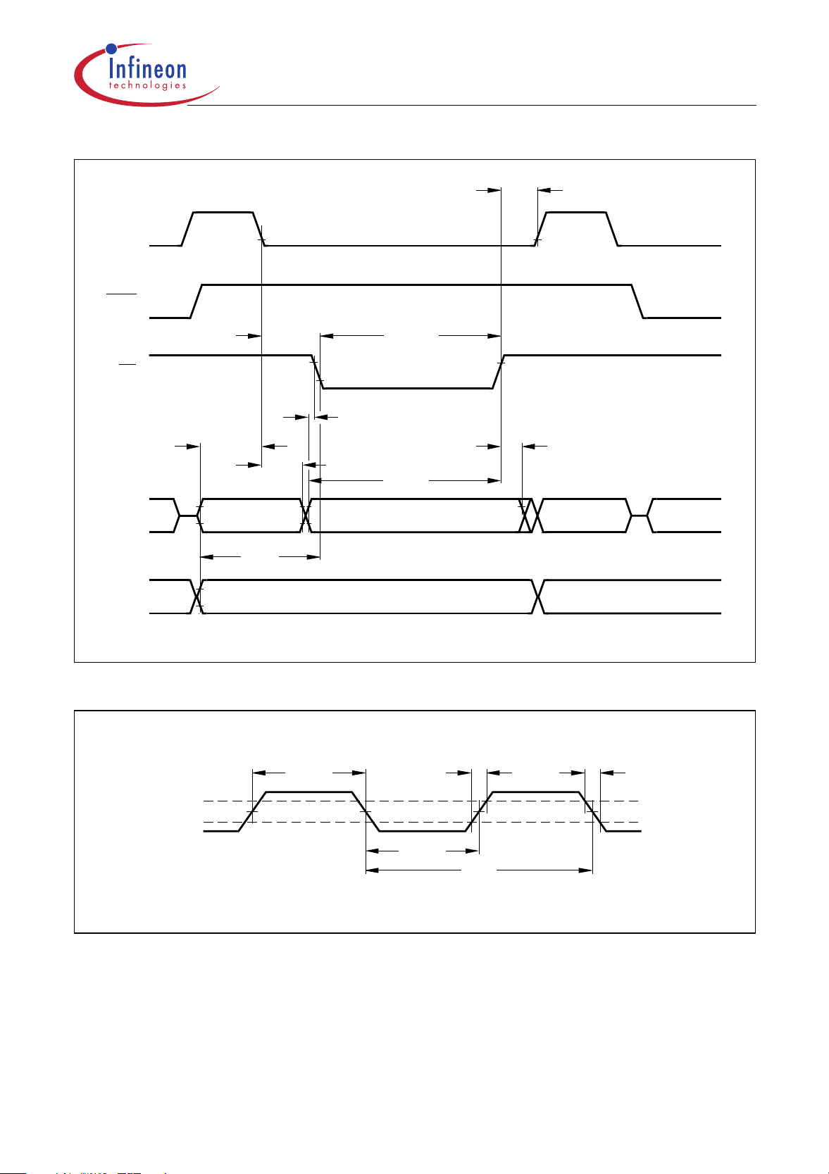
C515C
t
WHLH
ALE
PSEN
t
LLWL
WR
t
QVWX
t
Port 0
AVLL
A0 - A7 from
Ri or DPL from PCL
t
AVWL
t
LLAX2
Data OUT
Port 2
Figure 32 Data Memory Write Cycle
t
WLWH
t
QVWH
t
WHQX
A0 - A7
A8 - A15 from PCHP2.0 - P2.7 or A8 - A15 from DPH
Instr.IN
MCT00098
XTAL2
TCLH
t
R
t
F
V
IH2
V
IL
TCLL
CLP
MCT02704
Figure 33 External Clock Drive at XTAL2
Data Sheet 81 2003-02

C515C
t
SCLK
SCLK
STO
SRI
t
SCL
tt
D
t
SCH
~
~~
HD
~
MSB LSB
~
~
t
StHI
~
~
MSB LSB
~
~~
t
DTC
TC
~
MCT02417
Figure 34 SSC Timing
Notes:
1. Shown is the data/clock relationship for CPOL = CPHA = 1. The timing diagram is
valid for the other cases accordingly.
2. In the case of slave mode and CPHA = 0, the output delay for the MSB applies to the
falling edge of SLS
(if transmitter is enabled).
3. In the case of master mode and CPHA = 0, the MSB becomes valid after the data
has been written into the shift register, i.e. at least one half SCLK clock cycle before
the first clock transition.
Data Sheet 82 2003-02
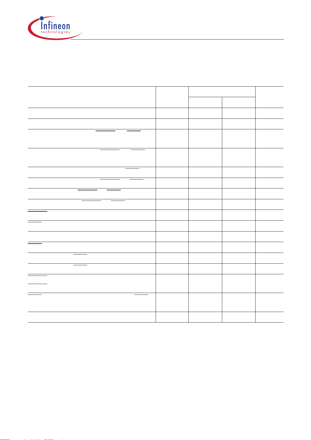
C515C
OTP Memory Programming Mode Characteristics
V
= 5 V ± 10%; VPP = 11.5 V ± 5%; TA = 25 °C ± 10 °C
DD
Parameter Symbol Limit Values Unit
min. max.
ALE pulse width
PMSEL setup to ALE rising edge
Address setup to ALE, PROG
, or PRD
falling edge
Address hold after ALE, PROG
, or PRD
falling edge
Address, data setup to PROG or PRD
Address, data hold after PROG
PMSEL setup to PROG
PMSEL hold after PROG
PROG
PRD
pulse width t
pulse width t
or PRD t
or PRD t
or PRD t
Address to valid data out
to valid data out t
PRD
Data hold after PRD
t
PAW
t
PMS
t
PAS
t
PAH
t
PCS
PCH
PMS
PMH
PWW
PRW
t
PAD
PRD
t
PDH
35 – ns
10 – ns
10 – ns
10 – ns
100 – ns
0–ns
10 – ns
10 – ns
100 – µs
100 – ns
–75ns
–20ns
0–ns
Data float after PRD
PROG
PROG
PRD
high between two consecutive
low pulses
high between two consecutive PRD
t
PDF
t
PWH1
t
PWH2
–20ns
1–µs
100 – ns
low pulses
XTAL clock period
Data Sheet 83 2003-02
t
CLKP
210MHz

C515C
t
PAW
PALE
t
PMS
PMSEL1,0
Port 2
Port 0
t
PAS
t
PAH
A8-15 A0-7
H, H
D0-7
PROG
t
PCS
t
PWW
PRD must be high during a programming write cycle.Notes:
Figure 35 Programming Code Byte - Write Cycle Timing
t
PCH
t
PWH
MCT03690
Data Sheet 84 2003-02

C515C
t
PAW
PALE
t
PMS
PMSEL1,0
Port 2
t
PAS
t
PAH
A8-15 A0-7
t
PAD
H, H
Port 0
t
PRD
t
PCS
t
PRW
Notes: PROG must be high during a programming read cycle.
Figure 36 Verify Code Byte - Read Cycle Timing
D0-7
t
PDH
t
t
PDFPRD
PCH
t
PWH
MCT03689
Data Sheet 85 2003-02
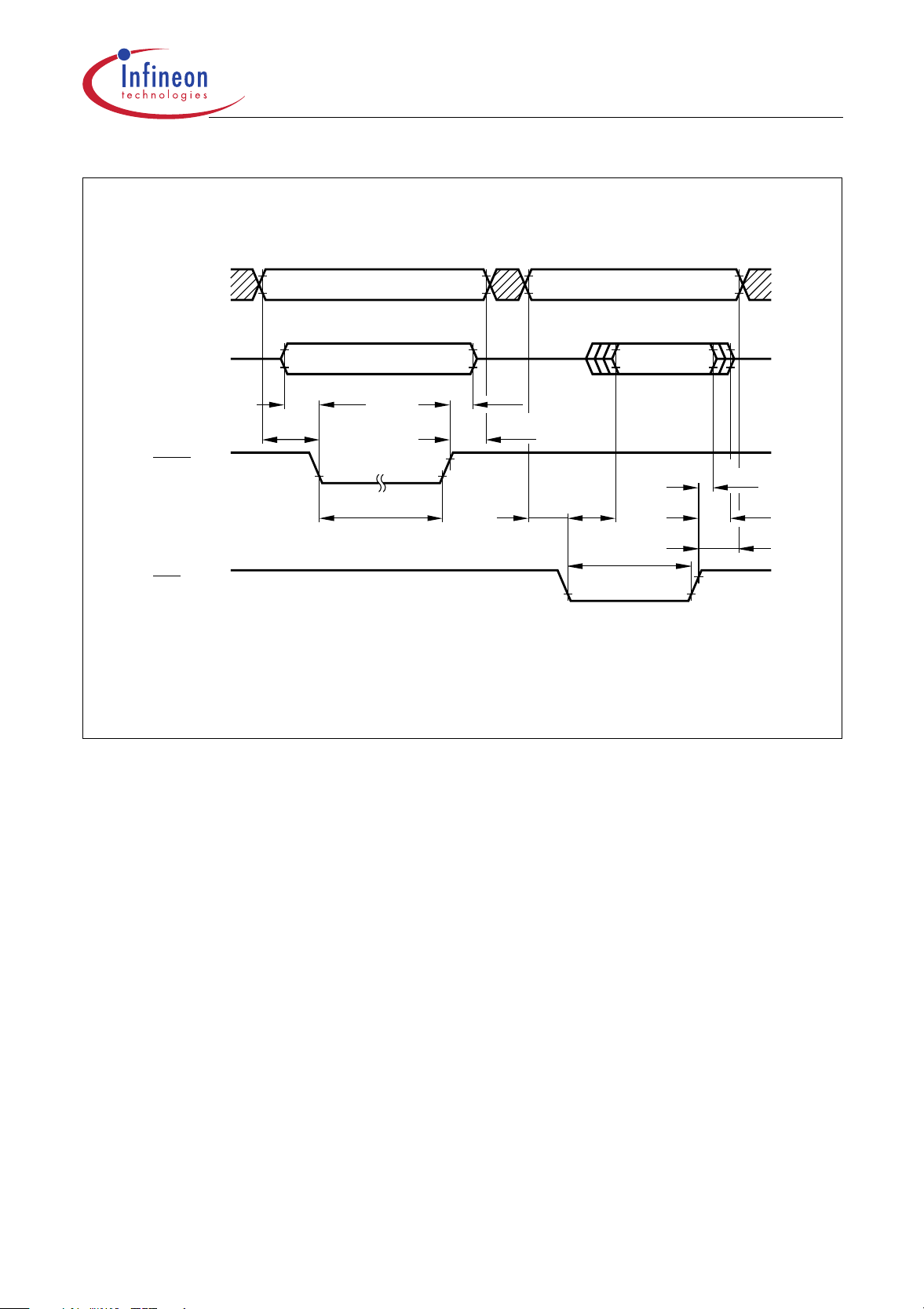
C515C
PMSEL1,0
Port 0
PROG
PRD
PALE should be low during a lock bit read / write cycle.Note:
t
PMS
H, L H, L
D0, D1 D0, D1
t
PCS
t
PWW
t
PCH
t
PMH
t
PMStPRD
t
PRW
t
PDH
t
t
PMH
MCT03393
PDF
Figure 37 Lock Bit Access Timing
Data Sheet 86 2003-02

C515C
PMSEL1,0
Port 2
Port 0
PRD
PROG must be high during a programming read cycle.Note:
t
t
PMS
PCS
L, H
e. g. FD
D0-7
t
PRD
t
PRW
H
t
PCH
t
PDH
t
PDF
t
PMH
MCT03394
Figure 38 Version Byte - Read Timing
Data Sheet 87 2003-02
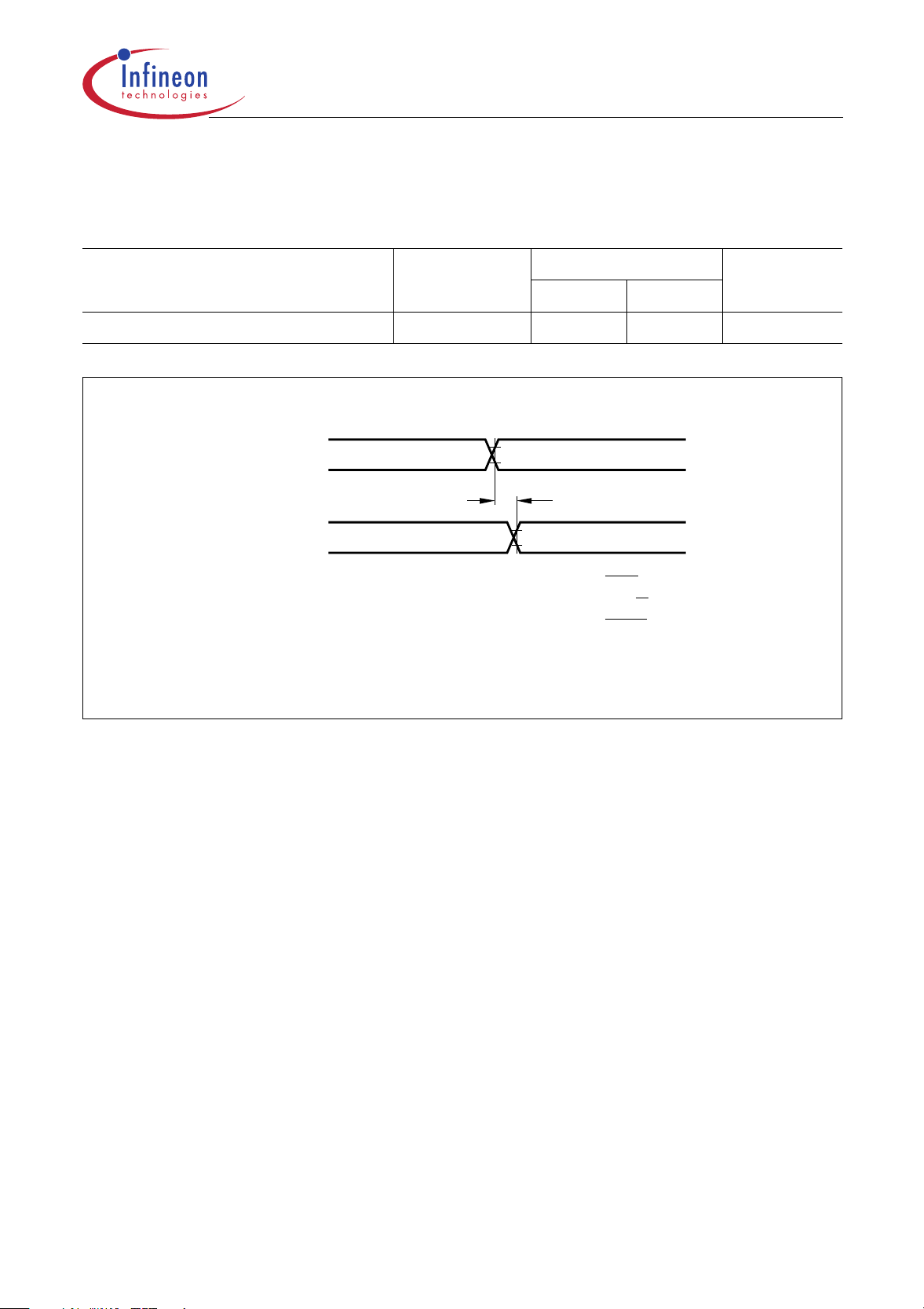
ROM/OTP Verification Characteristics for C515C-8R / C515C-8E
ROM Verification Mode 1 (C515C-8R)
Parameter Symbol Limit Values Unit
min. max.
C515C
Address to valid data
P1.0 - P1.7
P2.0 - P2.7
Port 0
Data:
Addresses:
P0.0 - P0.7 = D0 - D7
P1.0 - P1.7 = A0 - A7
P2.0 - P2.7 = A8 - A15
t
AVQV
Address
Data Out New Data Out
Figure 39 ROM Verification Mode 1
–5 CLPns
New Address
t
AVQV
Inputs: PSEN =SSV
ALE, EA
RESET =V
= V
IH
IL2
MCT02764
Data Sheet 88 2003-02
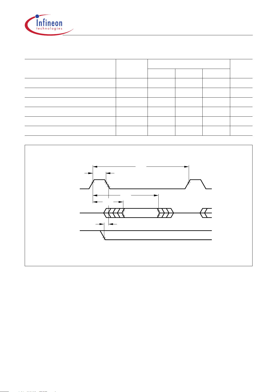
C515C
ROM/OTP Verification Mode 2
Parameter Symbol Limit Values Unit
min. typ. max.
ALE pulse width
ALE period
Data valid after ALE
Data stable after ALE
P3.5 setup to ALE low
t
AWD
t
ACY
t
DVA
t
DSA
t
AS
–CLP–ns
–6 CLP–ns
––2 CLPns
4 CLP––ns
– t
CL
–ns
Oscillator frequency 1 / CLP4–6MHz
t
ACY
t
AWD
ALE
t
DSA
t
DVA
Port 0
t
AS
Data Valid
P3.5
Figure 40 ROM/OTP Verification Mode 2
MCT02613
Data Sheet 89 2003-02
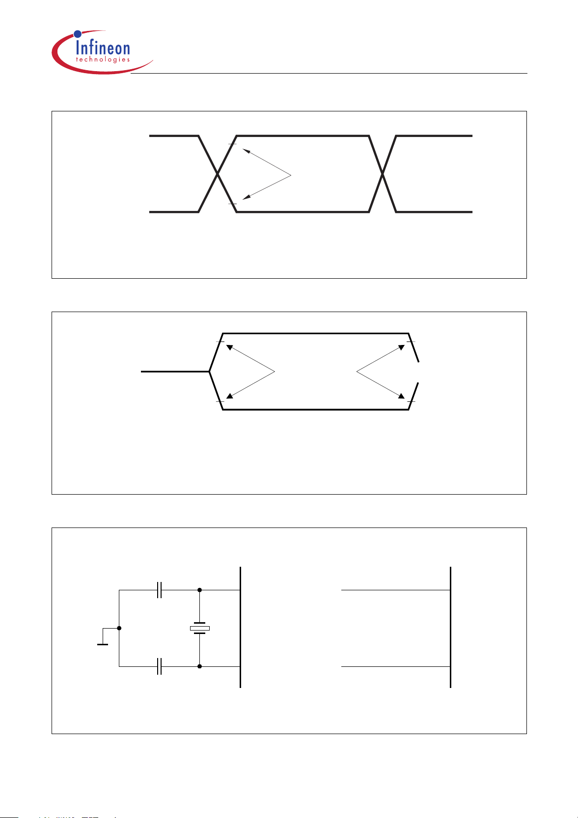
V
- 0.5 V
DD
+ 0.90.2
V
DD
Test Points
V
0.2 - 0.1
DD
0.45 V
MCT00039
AC Inputs during testing are driven at VDD - 0.5 V for a logic ‘1’ and 0.45 V for a logic ‘0’.
Timing measurements are made at
V
for a logic ‘1’ and V
IHmin
for a logic ‘0’.
ILmax
Figure 41 AC Testing: Input, Output Waveforms
C515C
-0.1 V
V
OH
+0.1 V
V
OL
MCT00038
V
Load
V
V
Load
Load
+0.1 V
Timing Reference
Points
-0.1 V
For timing purposes a port pin is no longer floating when a 100 mV change from load voltage
occurs and begins to float when a 100 mV change from the loaded
I
OL/IOH
≥ ± 20 mA
V
OH/VOL
level occurs.
Figure 42 AC Testing: Float Waveforms
Crystal/Resonator Oscillator Mode Driving from External Source
C
XTAL1
N.C.
XTAL1
2 - 10 MHz
C
Crystal Mode :
XTAL2 XTAL2
C = 20 pF ± 10 pF (incl. stray capacitance)
:Resonator Mode
= depends on selected ceramic resonatorC
External Oscillator
Signal
MCT02765
Figure 43 Recommended Oscillator Circuits for Crystal Oscillator
Data Sheet 90 2003-02
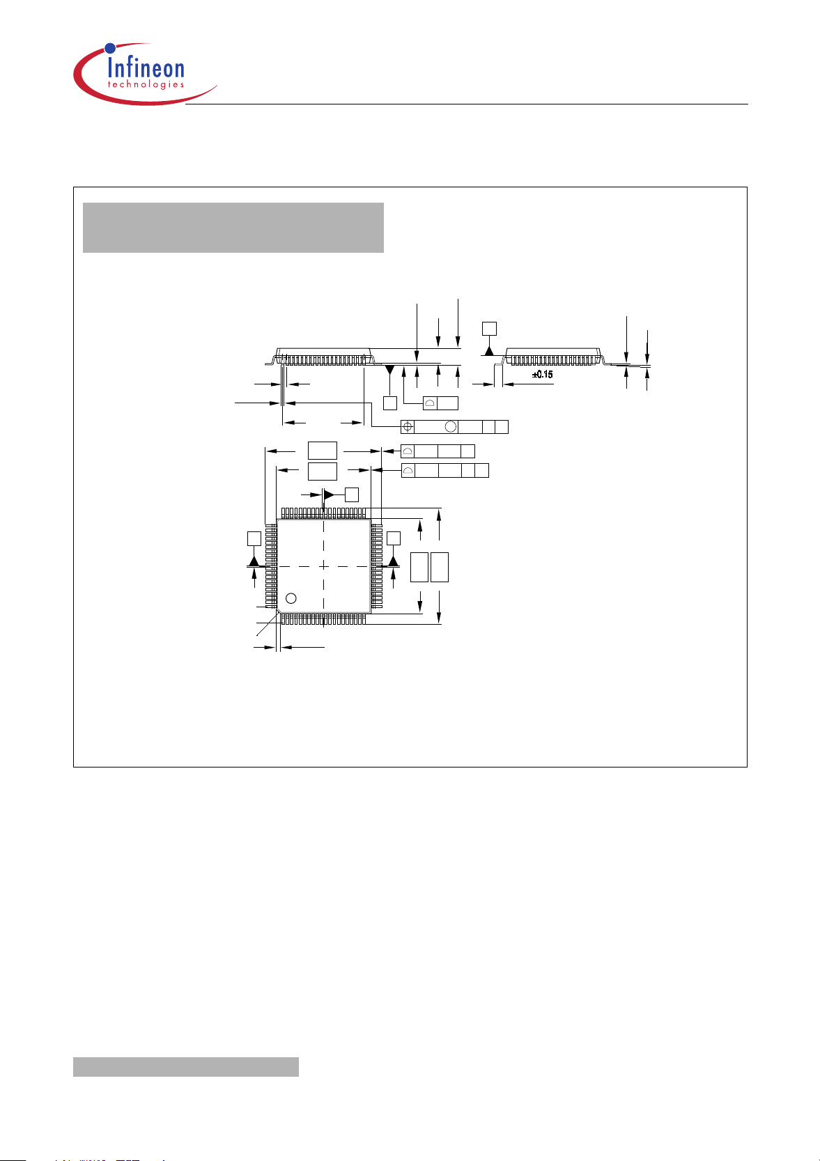
Package Outlines
P-MQFP-80-1
(Plastic Metric Quad Flat Package)
C515C
0.65
±0.08
0.3
12.35
17.2
1)
14
D
A
80
Index Marking
1) Does not include plastic or metal protrusions of 0.25 max per side
1
0.6x45˚
C
B
+0.1
-0.05
2.45 max
2
0.25 min
0.1
M
0.12
0.2
A-B
0.2
A-B
1)
17.2
14
A-B
D
80x
H
0.88
80x
D
C
4x
HD
-0.02
+0.08
0.15
7˚max
GPM05249
You can find all of our packages, sorts of packing and others in our
Infineon Internet Page “Products”: http://www.infineon.com/products.
SMD = Surface Mounted Device
Dimensions in mm
Data Sheet 91 2003-02

www.infineon.com
Published by Infineon Technologies AG
 Loading...