


Data Sheet, V2.0, Dec. 2000
C165
16-Bit Single-Chip Microcontroller
Microcontrollers
Never stop thinking.

Edition 2000-12
Published by Infineon Technologies AG,
St.-Martin-Strasse 53,
D-81541 München, Germa ny
© Infineon Technologies AG 2000.
All Rights Reserved.
Attention please!
The information herein is given to describe certain com ponents and shall not be consid ered as warranted
characteristics.
Terms of delivery and rights to technical change reserved.
We hereby disclaim any and all warranties, including but not limited to warranties of non-infringement, regarding
circuits, descriptions and charts stated her ein.
Infineon Technologies is an approved CECC manufacturer.
Information
For further information on te ch nology, delivery terms and conditions and prices please contact your nearest
Infineon Technologies Office in Germany or ou r Infineon Technologies Representatives worldwide.
Warnings
Due to technical requirements co mp onents may contain dangerous substan ce s. For information on the typ es in
question please contact your nearest Infineon Technologies Office.
Infineon Technologies Components may only be used in life-support devices or systems with the express written
approval of Infineon T echnologies, if a f ailure of such components can reasonably be expected to cause the failure
of that life - su ppo rt de vi ce o r system, or to aff ec t th e sa fety or effectiveness of that devi ce o r system. Life supp ort
devices or systems are intended to be implanted in the human body, or to support and/or maintain and sustain
and/or protect human life. If they fail, it is reasonable to assume that the health of the user or other persons may
be endangered.

Data Sheet, V2.0, Dec. 2000
C165
16-Bit Single-Chip Microcontroller
Microcontrollers
Never stop thinking.
C165
Revision History: 2000-12 V2.0
Previous Version: 1998-12 Update 0.5µ technology
01.96 3 Volt Addendum
07.95 25 MHz Addendum
09.94 Data Sheet
Page Subjects (major changes since last revision)
All Converted to Infineon layout
2 ROM derivatives removed, 25-MHz derivatives and 3 V derivatives
included
6ff Pin numbers for TQFP added
14 Address window arbitration and master/slave mode introduced
32 New standard layout for section “Absolute Maximum Ratings”
33 Section “Operating Condition s” added
34f Parameter “RSTIN
pullup” replaced by “RSTIN current”
36f DC Characteristics for reduced supply voltage added
38f Separate specification for power consumption with greatly improved values
40ff Description of clock generation improved
45, 55, 65 Timing adapted to 25 MHz
48, 58, 66 Timing for reduced supply voltage added
We Listen to Your Comments
Any information within this document that you feel is wrong, unclear or missing at all?
Your feedback will help us to continuously improve the quality of this document.
Please send your proposal (including a reference to this document) to:
mcdocu.comments@infineon.com

C166 Family
C165
• High Performance 16-bit CPU with 4-Stage Pipeline
– 80 ns Instruction Cycle Time at 25 MHz CPU Clock
– 400 ns Multiplication (16 × 16 bit), 800 ns Division (32 / 16 bit)
– Enhanced Boolean Bit Manipulation Facilities
– Additional Instructions to Support HLL and Operating Systems
– Register-Based Design with Multiple Variable Register Banks
– Single-Cycle Context Switching Support
– 16 MBytes Total Linear Address Space for Code and Data
– 1024 Bytes On-Chip Special Function Register Area
• 16-Priority-Level Interrupt System with 28 Sources, Sample-Rate down to 40 ns
• 8-Channel Interrupt-Driven Single-Cycle Data Transfer Facilities via
Peripheral Event Controller (PEC)
• Clock Generation via prescaler or via direct clock input
• On-Chip Memory Modules
– 2 KBytes On-Chip Internal RAM (IRAM)
• On-Chip Peripheral Modules
– Two Multi-Functional General Purpose Timer Units with 5 Timers
– Two Serial Channels (Synchronous/Asynchronous and High-Speed-Synchronous)
• Up to 16 MBytes External Address Space for Code and Data
– Programmable External Bus Characteristics for Different Address Ranges
– Multiplexed or Demultiplexed External Address/Data Buses with 8-Bit or 16-Bit
Data Bus Width
– Five Programmable Chip-Select Signals
– Hold- and Hold-Acknowledge Bus Arbitration Support
• Idle and Power Down Modes
• Programmable Watchdog Timer
• Up to 77 General Purpose I/O Lines,
partly with Selectable Input Thresholds and Hysteresis
• Power Supply: the C165 can operate from a 5 V or a 3 V power supply
• Supported by a Large Range of Development Tools like C-Compilers,
Macro-Assembler Packages, Emulators, Evaluation Boards, HLL-Debuggers,
Simulators, Logic Analyzer Disassemblers, Programming Boards
• On-Chip Bootstrap Loader
• 100-Pin MQFP Package (0.65 mm pitch)
• 100-Pin TQFP Package (0.5 mm pitch)
C16516-Bit Single-Chip Microcontroller
Data Sheet 1 V2.0, 2000-12
C165
This document describes several derivatives of the C165 grou p. Table 1 enumerates
these derivatives and summarizes the differences. As this document refers to all of these
derivatives, some descriptions may not apply to a specific product.
Table 1 C165 Derivative Synopsis
Derivative
1)
SAF-C165-LM 20 MHz 4.5 to 5.5 V MQFP-100
SAB-C165-LM 20 MHz 4.5 to 5.5 V MQFP-100
SAF-C165-L25M 25 MHz 4.5 to 5.5 V MQFP-100
SAB-C165-L25M 25 MHz 4.5 to 5.5 V MQFP-100
SAF-C165-LF 20 MHz 4.5 to 5.5 V TQFP-100
Max. Operating
Frequency
Operating
Voltage
Package
SAB-C165-LF 20 MHz 4.5 to 5.5 V TQFP-100
SAF-C165-L25F 25 MHz 4.5 to 5.5 V TQFP-100
SAB-C165-L25F 25 MHz 4.5 to 5.5 V TQFP-100
SAF-C165-LM3V 20 MHz 3.0 to 3.6 V MQFP-100
SAB-C165-LM3V 20 MHz 3.0 to 3.6 V MQFP-100
SAF-C165-LF3V 20 MHz 3.0 to 3.6 V TQFP-100
SAB-C165-LF3V 20 MHz 3.0 to 3.6 V TQFP-100
1)
This Data Sheet is valid for devic es start ing with and including design st ep H A.
For simplicity all versions are referred to by the term C165 throughout this document.
Ordering Information
The ordering code for Infineon microcontrollers provides an exact reference to the
required product. This ordering code identifies:
• the derivative itself, i.e. its function set, the temperature range, and the supply voltage
• the package and the type of delivery.
For the available ordering codes for the C165 please refer to the “Product Catalog
Microcontrollers”, which summarizes all available microcontroller variants.
Note: The ordering codes for Mask-ROM versions are defined for each product after
verification of the respective ROM code.
Data Sheet 2 V2.0, 2000-12
C165
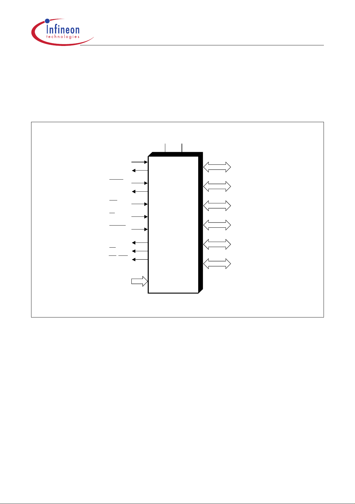
Introduction
The C165 is a derivativ e of the Infineon C1 66 Family of full featured si ngle -chi p CMOS
microcontrollers. It combin es high CPU perfo rman ce (up to 12 .5 mi llion instructions per
second) with peripheral functionality and enhanced IO-capabilities. The C165 is
especially suited for cost sensitive applications.
V
V
DD
SS
XTAL1
XTAL2
RSTIN
RSTOUT
NMI
EA
READY
ALE
RD
WR/WRL
Port 5
6 Bit
Figure 1 Logic Symbol
C165
Port 0
16 Bit
Port 1
16 Bit
Port 2
8 Bit
Port 3
15 Bit
Port 4
8 Bit
Port 6
8 Bit
MCL04824
Data Sheet 3 V2.0, 2000-12
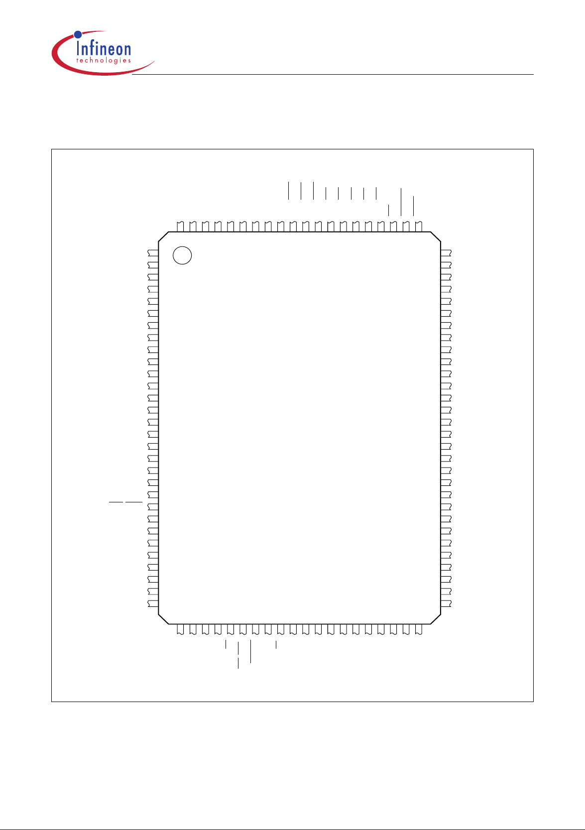
Pin Configuration TQFP Package
(top view)
P5.12/T6IN
P5.10/T6EUD
P2.15/EX7IN
P2.14/EX6IN
P2.13/EX5IN
P5.11/T5EUD
P2.12/EX4IN
P2.11/EX3IN
P2.10/EX2IN
P2.9/EX1IN
P2.8/EX0IN
P6.7/BREQ
P6.6/HLDA
P6.5/HOLD
P6.4/CS4
P6.3/CS3
P6.2/CS2
P6.1/CS1
P6.0/CS0
NMI
RSTOUT
DD
RSTIN
V
SS
P1H.7/A15
V
C165
P5.13/T5IN
P5.14/T4EUD
P5.15/T2EUD
V
SS
XTAL1
XTAL2
V
DD
P3.0
P3.1/T6OUT
P3.2/CAPIN
P3.3/T3OUT
P3.4/T3EUD
P3.5/T4IN
P3.6/T3IN
P3.7/T2IN
P3.8/MRST
P3.9/MTSR
P3.10/TxD0
P3.11/RxD0
P3.12/BHE/WRH
P3.13/SCLK
P3.15/CLKOUT
P4.0/A16
P4.1/A17
P4.2/A18
1
2
3
4
5
6
7
8
9
10
11
12
13
14
15
16
17
18
19
20
21
22
23
24
25
100
26
27
828384858687888990919293949596979899
81
80
C165
2928
32 33 34 35 36 37 38 39 40
30
41 424344
45 464748 49
76777879
75
74
73
72
71
70
69
68
67
66
65
64
63
62
61
60
59
58
57
56
55
54
53
52
51
5031
P1H.6/A14
P1H.5/A13
P1H.4/A12
P1H.3/A11
P1H.2/A10
V
SS
V
DD
P1H.1/A9
P1H.0/A8
P1L.7/A7
P1L.6/A6
P1L.5/A5
P1L.4/A4
P1L.3/A3
P1L.2/A2
P1L.1/A1
P1L.0/A0
P0H.7/AD15
P0H.6/AD14
P0H.5/AD13
P0H.4/AD12
P0H.3/AD11
P0H.2/AD10
P0H.1/AD9
P0H.0/AD8
DD
SS
V
V
P4.3/A19
P4.5/A21
P4.6/A22
P4.4/A20
RD
P4.7/A23
WR/WRL
ALE
READY
EA
SS
V
V
N.C.
P0L.2/AD2
P0L.0/AD0
P0L.1/AD1
P0L.3/AD3
P0L.6/AD6
P0L.5/AD5
P0L.4/AD4
SS
DD
V
V
P0L.7/AD7
MCP02216
DD
Figure 2
Data Sheet 4 V2.0, 2000-12
Pin Configuration MQFP Package
(top view)
P2.15/EX7IN
P2.14/EX6IN
P2.13/EX5IN
P2.12/EX4IN
P2.11/EX3IN
P2.10/EX2IN
P2.9/EX1IN
P2.8/EX0IN
P6.7/BREQ
P6.6/HLDA
P6.5/HOLD
P6.4/CS4
P6.3/CS3
P6.2/CS2
P6.1/CS1
P6.0/CS0
NMI
RSTOUT
C165
RSTIN
99 98 97 96 95 94 93 92 91 90 89 88 87 86 85 84 83 82100
P5.11/T5EUD
P5.12/T6IN
P5.13/T5IN
P5.14/T4EUD
P5.15/T2EUD
V
XTAL1
XTAL2
V
P3.0
P3.1/T6OUT
P3.2/CAPIN
P3.3/T3OUT
P3.4/T3EUD
P3.5/T4IN
P3.6/T3IN
P3.7/T2IN
P3.8/MRST
P3.9/MTSR
P3.10/TxD0 P1L.0/A0
P3.11/RxD0
P3.12/BHE/WRH
P3.13/SCLK
P3.15/CLKOUT
P4.0/A16
P4.1/A17
P4.2/A18
P4.3/A19
V
V
SS
DD
SS
DD
1
2
3
4
5
6
7
8
9
10
11
12
13
14
15
16
17
18
19
20
21
22
23
24
25
26
27
28
29
30
C165
403938373635343332
44
4645
47
43
4241
81
80
79
78
77
76
75
74
73
72
71
70
69
68
67
66
65
64
63
62
61
60
59
58
57
56
55
54
53
52
51
5031
4948
V
DD
V
SS
P1H.7/A15
P1H.6/A14
P1H.5/A13
P1H.4/A12
P1H.3/A11
P1H.2/A10
V
SS
V
DD
P1H.1/A9
P1H.0/A8
P1L.7/A7
P1L.6/A6
P1L.5/A5
P1L.4/A4
P1L.3/A3
P1L.2/A2
P1L.1/A1
P0H.7/AD15
P0H.6/AD14
P0H.5/AD13
P0H.4/AD12
P0H.3/AD11
P0H.2/AD10
P0H.1/AD9
P0H.0/AD8
V
SS
V
DD
ALE
READY
EA
V
V
N.C.
P0L.2/AD2
P0L.0/AD0
P0L.1/AD1
P0L.5/AD5
P0L.3/AD3
P0L.4/AD4
P0L.6/AD6
P0L.7/AD7
MCP02144
P4.5/A21
P4.6/A22
P4.4/A20 P5.10/T6EUD
P4.7/A23
RD
WR/WRL
SS
DD
Figure 3
Data Sheet 5 V2.0, 2000-12
Table 2 Pin Definitions and Functions
C165
Symbol Pin Nr
TQFP
XTAL1
XTAL256
P3
P3.0
P3.1
P3.2
P3.3
P3.4
P3.5
P3.6
P3.7
P3.8
P3.9
P3.10
P3.11
P3.12
P3.13
P3.15
8
9
10
11
12
13
14
15
16
17
18
19
20
21
22
Pin Nr
MQFP
7
8
10
11
12
13
14
15
16
17
18
19
20
21
22
23
24
Input
Outp.
I
O
IO
O
I
O
I
I
I
I
I/O
I/O
O
I/O
O
O
I/O
O
Function
XTAL1: Input to the oscillator amplifier and input
to the internal clock generator
XTAL2: Output of the oscillator amplifier circuit.
To clock the device from an external source, drive
XTAL1, while leaving XTAL2 unconnected.
Minimum and maximum high/low and rise/fall times
specified in the AC Characteristics must be
observed.
Port 3 is a 15-bit bidirectional I/O port. It is bit-wise
programmable for input or output via direction bits.
For a pin configured as input, the output driver is put
into high-impedance state. Port 3 outputs can be
configured as push/pull or open drain drivers. The
Port 3 pins serve for following alternate functions:
T6OUT GPT2 Timer T6 Toggle Latch Output
CAPIN GPT2 Register CAPREL Capture Input
T3OUT GPT1 Timer T3 Toggle Latch Output
T3EUD GPT1 Timer T3 Ext. Up/Down Ctrl Input
T4IN GPT1 Timer T4
Count/Gate/Reload/Capture Input
T3IN GPT1 Timer T3 Count/Gate Input
T2IN GPT1 Timer T2
Count/Gate/Reload/Capture Input
MRST SSC Master-Receive/Slave-Transmit
Input/Output
MTSR SSC Master-Transmit/Slave-Receive
Output/Input
TxD0 ASC0 Clock/Data Output (Asyn./Sync.)
RxD0 ASC0 Data Inp. (Asyn.) or In/Out (Sync)
BHE
WRH
Ext. Memory High Byte Enable Signal,
Ext. Memory High Byte Write Strobe
SCLK SSC Master Cl. Output / Slave Cl. Input
CLKOUT System Clock Output (= CPU Clock)
Data Sheet 6 V2.0, 2000-12
Table 2 Pin Definitions and Functions (cont’d)
C165
Symbol Pin Nr
TQFP
P4
P4.0
P4.1
P4.2
P4.3
P4.4
P4.5
P4.6
P4.7
RD
WR
/
23
24
25
26
29
30
31
32
33 35 O External Memory Read Strobe. RD is activated for
34 36 O External Memory Write Strobe. In WR-mode this pin
WRL
Pin Nr
MQFP
25
26
27
28
31
32
33
34
Input
Outp.
IO
O
O
O
O
O
O
O
O
Function
Port 4 is an 8-bit bidirectional I/O port. It is bit-wise
programmable for input or output via direction bits.
For a pin configured as input, the output driver is put
into high-impedance state. Port 4 can be used to
output the segment address lines:
A16 Least Significant Segment Address Line
A17 Segment Address Line
A18 Segment Address Line
A19 Segment Address Line
A20 Segment Address Line
A21 Segment Address Line
A22 Segment Address Line
A23 Most Significant Segment Address Line
every external instruction or data read access.
is activated for every external data write access. In
-mode this pin is activated for low byte data
WRL
write accesses on a 16-bit bus, and for every data
write access on an 8-bit bus. See WRCFG in register
SYSCON for mode selection.
READY
35 37 I Ready Input. When the Ready function is enabled, a
high level at this pin during an external memory
access will force the insertion of memory cycle
waitstates until the pin returns to a low level.
An internal pullup device holds this pin high when
nothing is driving it.
ALE 36 38 O Address Latch Enable Output. Can be used for
latching the address into external memory or an
address latch in the multiplexed bus modes.
EA
37 39 I External Access Enable pin. A low level at this pin
during and after Reset forces the C165 to begin
instruction execution out of external memory. A high
level forces execution out of the internal program
memory.
“ROMless” versions must have this pin tied to ‘0’.
Data Sheet 7 V2.0, 2000-12

Table 2 Pin Definitions and Functions (cont’d)
C165
Symbol Pin Nr
TQFP
Pin Nr
MQFP
Input
Outp.
Function
NC 40 42 – This pin is not connected in the C165.
No connection to the PCB is required.
PORT0
P0L.0-7
41-48
43-50
IO PORT0 consists of the two 8-bit bidirectional I/O
ports P0L and P0H. It is bit-wise programmable for
input or output via direction bits. For a pin configured
P0H.0-7
51-58
53-60
as input, the output driver is put into high-impedance
state. In case of an external bus configuration,
PORT0 serves as the address (A) and address/data
(AD) bus in multiplexed bus modes and as the data
(D) bus in demultiplexed bus modes.
Demultiplexed bus modes:
Data Path Width: 8-bit 16-bit
P0L.0 – P0L.7: D0 – D7 D0 – D7
P0H.0 – P0H.7: I/O D8 – D15
Multiplexed bus modes:
Data Path Width: 8-bit 16-bit
P0L.0 – P0L.7: AD0 – AD7 AD0 – AD7
P0H.0 – P0H.7: A8 – A15 AD8 – AD15
PORT1
P1L.0-7
P1H.0-7
59-66
67,68,
71-76
61-68
69-70,
73-78
IO PORT1 consists of the two 8-bit bidirectional I/O
ports P1L and P1H. It is bit-wise programmable for
input or output via direction bits. For a pin configured
as input, the output driver is put into high-impedance
state. PORT1 is used as the 16-bit address bus (A)
in demultiplexed bus modes and also after switching
from a demultiplexed bus mode to a multiplexed bus
mode.
Data Sheet 8 V2.0, 2000-12
Table 2 Pin Definitions and Functions (cont’d)
C165
Symbol Pin Nr
TQFP
Pin Nr
MQFP
Input
Outp.
Function
RSTIN 79 81 I/O Reset Input with Schmitt-Trigger characteristics. A
low level at this pin while the oscillator is running
resets the C165. An internal pullup resistor permits
power-on reset using only a capacitor connected to
V
. A spike filter suppresses input pulses < 10 ns.
SS
Input pulses >100 ns safely pass the filter. The
minimum duration for a safe recognition should be
100 ns + 2 CPU clock cycles.
In bidirectional reset mode (enabled by setting bit
BDRSTEN in register SYSCON) the RSTIN
line is
internally pulled low for the duration of the internal
reset sequence upon any reset (HW, SW, WDT).
See note below this table.
Note: To let the reset configuration of PORT0 settle
a reset duration of ca. 1 ms is recommended.
RST
OUT
80 82 O Internal Reset Indication Output. This pin is set to a
low level when the part is executing either a
hardware-, a software- or a watchdog timer reset.
RSTOUT
remains low until the EINIT (end of
initialization) instruction is executed.
NMI
81 83 I N on-Maskable Interrupt Input. A high to low
transition at this pin causes the CPU to vector to the
NMI trap routine. When the PWRDN (power down)
instruction is executed, the NMI
pin must be low in
order to force the C165 to go into power down mode.
If NMI
is high, when PWRDN is exec uted, the part
will continue to run in normal mode.
If not used, pin NMI
should be pulled high externally.
Data Sheet 9 V2.0, 2000-12
Table 2 Pin Definitions and Functions (cont’d)
C165
Symbol Pin Nr
TQFP
P6
P6.0
P6.1
P6.2
P6.3
P6.4
P6.5
P6.6
P6.7
82
83
84
85
86
87
88
89
P2
P2.8
P2.9
P2.10
P2.11
P2.12
P2.13
P2.14
P2.15
90
91
92
93
94
95
96
97
Pin Nr
MQFP
84
85
86
87
88
89
90
91
92
93
94
95
96
97
98
99
Input
Outp.
IO
O
O
O
O
O
I
I/O
O
IO
I
I
I
I
I
I
I
I
Function
Port 6 is an 8-bit bidirectional I/O port. It is bit-wise
programmable for input or output via direction bits.
For a pin configured as input, the output driver is put
into high-impedance state. Port 6 outputs can be
configured as push/pull or open drain drivers.
The Port 6 pins also serve for alternate functions:
CS0
CS1
CS2
CS3
CS4
HOLD
HLDA
Chip Select 0 Output
Chip Select 1 Output
Chip Select 2 Output
Chip Select 3 Output
Chip Select 4 Output
External Master Hold Request Input
Hold Acknowledge Outp.(master mode)
or Input (slave mode)
BREQ
Bus Request Output
Port 2 is an 8-bit bidirectional I/O port. It is bit-wise
programmable for input or output via direction bits.
For a pin configured as input, the output driver is put
into high-impedance state. Port 2 outputs can be
configured as push/pull or open drain drivers. The
following Port 2 pins serve for alternate functions:
EX0IN Fast External Interrupt 0 Input
EX1IN Fast External Interrupt 1 Input
EX2IN Fast External Interrupt 2 Input
EX3IN Fast External Interrupt 3 Input
EX4IN Fast External Interrupt 4 Input
EX5IN Fast External Interrupt 5 Input
EX6IN Fast External Interrupt 6 Input
EX7IN Fast External Interrupt 7 Input
P5
I
Port 5 is a 6-bit input-only port with Schmitt-Trigger
char. The pins of Port 5 also serve as timer inputs:
P5.10
P5.11
P5.12
P5.13
P5.14
P5.15
Data Sheet 10 V2.0, 2000-12
98
99
100
1
2
3
100
1
2
3
4
5
I
I
I
I
I
I
T6EUD GPT2 Timer T6 Ext. Up/Down Ctrl Input
T5EUD GPT2 Timer T5 Ext. Up/Down Ctrl Input
T6IN GPT2 Timer T6 Count Input
T5IN GPT2 Timer T5 Count Input
T4EUD GPT1 Timer T4 Ext. Up/Down Ctrl Input
T2EUD GPT1 Timer T2 Ext. Up/Down Ctrl Input
Table 2 Pin Definitions and Functions (cont’d)
C165
Symbol Pin Nr
TQFP
V
DD
7, 28,
38,
49,
69, 78
V
SS
4, 27,
39,
50,
Pin Nr
MQFP
9, 30,
40, 51,
71, 80
6, 29,
41, 52,
72, 79
Input
Function
Outp.
– Digital Supply Voltage:
+ 5 V or + 3 V during normal operation and idle
mode.
2.5 V during power down mode.
≥
– Digital Ground.
70, 77
Note: The following behavioural differences must be observed when the bidirectional
reset is active:
• Bit BDRSTEN in register SYSCON cannot be changed after EINIT and is cleared
automatically after a reset.
• The reset indication flags always indicate a long hardware reset.
• The PORT0 c onfig uration is tr eated l ike on a hardw are res et. Espe ciall y the bo otstra p
loader may be activated when P0L.4 is low.
•Pin RSTIN
may only be connected to external reset devices with an open drain output
driver.
• A short hardware reset is extended to the duration of the internal reset sequence.
Data Sheet 11 V2.0, 2000-12
C165
Functional Description
The architecture of the C165 combines advantages of both RISC and CISC processors
and of advanced peripheral subsystems in a very well-balanced way. In addition the
on-chip memory blocks allow the design of compact systems with maximum
performance.
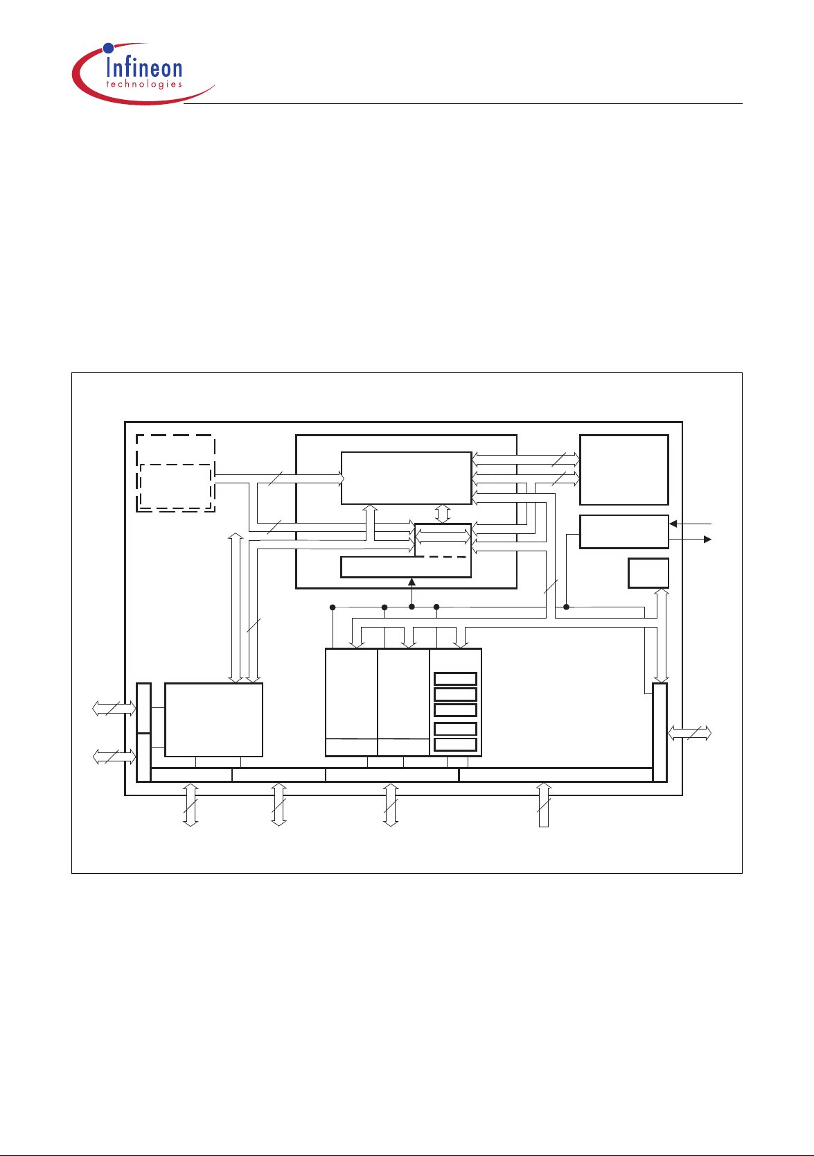
The following block diagram gives an overview of the different on-chip components and
of the advanced, high bandwidth internal bus structure of the C165.
Note: All time specifications refer to a CPU clock of 25 MHz
(see definition in the AC Characteristics section).
8
8
ProgMem
Internal
ROM
Area
XBUS Control
Port 4
External Bus
Control
Port 6
Port 0
EBC
16
32
Instr. / Data
16
16
On-Chip XBUS (16-Bit Demux)
Port 1
16
External Instr. / Data
Interrupt Controller
ASC0
(USART)
BRGen
C166-Core
CPU
SSC
(SPI)
BRGen
15
PEC
16-Level
Priority
GPT
T2
T3
T4
T5
T6
Interrupt Bus
Peripheral Data Bus
Data
Data
16
16
IRAM
Internal
Dual Port
2 KByte
Osc
RAM
XTAL
WDT
16
8
Port 2
Port 5Port 3
6
Figure 4 Block Diagram
The program memory, the internal R AM (IRAM) and the set of generic peripherals are
connected to the CPU via separate buses. A fourt h bus, the XBUS, connects ext ernal
resources as well as additional on-chip resoures, the X-Peripherals (see Figure 4).
Data Sheet 12 V2.0, 2000-12

C165
Memory Organization
The memory space of the C165 is configured in a Von Neumann architecture which
means that code memory, data memory, registers and I/O ports are organized within the
same linear address space which includes 16 MBytes. The entire memory space can be
accessed bytewise or wordwise. Particular portions of the on-chip memory have
additionally been made directly bitaddressable.
The C165 is prepared to incorporate on-chip program memory (not in the ROM-less
derivatives, of course) for code or constant data. The internal ROM area can be mapped
either to segment 0 or segment 1.
2 KBytes of on-chip Internal RAM (IRAM) are provided as a storage for user defined
variables, for th e system stack, general purpo se register banks and even for code. A
register bank can consist of up to 16 wordwide (R0 to R15) and/or bytewide (RL0, RH0,
…, RL7, RH7) so-called General Purpose Registers (GPRs).
1024 bytes (2×512 bytes) of the address space are reserved for the Special Func tion
Register areas (SFR space and ESFR sp ace). SFRs are w ordwide registers which are
used for controlling and monitoring functions of the different on-chip units. Unused SFR
addresses are reserved for future members of the C166 Family.
In order to meet the n eed s of d esi gns w he re m ore m emo ry is required than is provi ded
on chip, up to 16 MBytes of external RAM and/or ROM can be connected to the
microcontroller.
Data Sheet 13 V2.0, 2000-12

C165
External Bus Controller
All of the external memory accesses are performed by a particular on-chip External Bus
Controller (EBC). It can be programmed either to Single Chi p Mode when no external
memory is required, or to one of four different external memory access modes, which are
as follows:
– 16-/18-/20-/24-bit Addresses, 16-bit Data, Demultiplexed
– 16-/18-/20-/24-bit Addresses, 16-bit Data, Multiplexed
– 16-/18-/20-/24-bit Addresses, 8-bit Data, Multiplexed
– 16-/18-/20-/24-bit Addresses, 8-bit Data, Demultiplexed
In the demultiplexed bus modes, addresses are output on PORT1 and data is input/
output on PORT0 or P0L, respectively. In the mul tiplexed bus modes both addresses
and data use PORT0 for input/output.
Important timing characteristics of the external bus interface (Memory Cycle Time,
Memory Tri-State Time, Length of ALE and Read Write Delay) have been made
programmable to allow the user the adaption of a wide range of different types of
memories and external peripherals.
In addition, up to 4 indepen dent address windows may be defined (via register pairs
ADDRSELx / BUSCONx) which co ntrol the access to diff erent resources with different
bus characteristics. These address windows are arranged hierarchically where
BUSCON4 overrides BUSCON3 and BUSCON2 overrides BUSCON1. All accesses to
locations not covered by these 4 address windows are controlled by BUSCON0.
Up to 5 external CS
external glue logic. The C165 offers the possibility to switch the CS
unlatched mode. In this m ode the intern al filter logic is switched o ff and the CS
are directly genera ted from the address . The u nlatch ed CS
signals (4 windows plus de fault) can be generated in order to save
outputs to an
signals
mode is enabled by setting
CSCFG (SYSCON.6).
Access to very sl ow m emories or me morie s wi th va ry ing a ccess times i s sup ported via
a particular ‘Ready’ function.
A HOLD
/HLDA protocol is available for bus arbitration and allows to share external
resources with other bus ma sters. The bus arbitration is en abled by setting bit HLDEN
in register PSW. After setting HLDEN once, pins P6.7 … P6.5 (BREQ
, HLDA, HOLD)
are automatically controlled by the EBC. In Master M ode (def ault after reset) the HLDA
pin is an output. By setti ng bit DP6.7 to ‘1’ th e Sla ve Mod e is s elec ted w here pin HLD A
is switched to input. This allows to directly connect the slave controller to another master
controller without gl ue logic.
For applications which require less than 16 MBytes of external memory space, this
address space can be restricted to 1 MByte, 256 KByte, or to 64 KByte. In this case
Port 4 ou tputs four, two, or no address lines at all. It outputs all 8 address lines, if an
address space of 16 MBytes is used.
Data Sheet 14 V2.0, 2000-12
C165
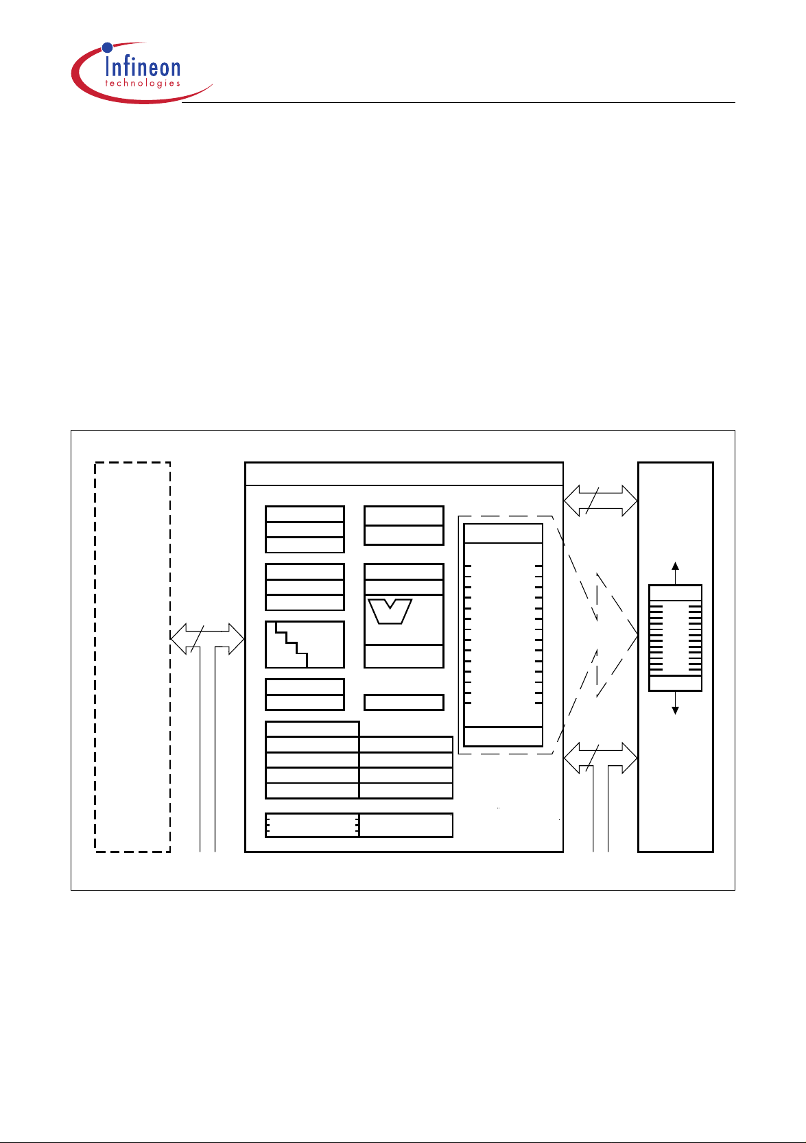
Central Processing Unit (CPU)
The main core of the C PU consis ts of a 4 -stage inst ructi on pipelin e, a 16-b it arithmetic
and logic unit (ALU) and dedicated SFRs. Additional hardware has been spent for a
separate multiply and divide unit, a bit-mask generator and a barrel shifter.
Based on these hardware prov isions, most of the C165’s instructions c an be executed
in just one machine cycle which requires 80 ns at 25 MHz CPU clock. For example, shift
and rotate instructions are al ways proce ssed du ring one m achine c ycle in dep endent of
the number of bits to be shifted. All multiple-cycle instructio ns have been optimized so
that they can be executed very fast as well: branches in 2 cycles, a 16×16 bit
multiplication in 5 cycles and a 32-/16 bit division in 10 cycles. Another pipeline
optimization, the so-called ‘Jump Cache’, allows reducing the execution time of
repeatedly performed jumps in a loop from 2 cycles to 1 cycle.
ROM
32
CPU
SP
STKOV
STKUN
Exec. Unit
Instr. Ptr.
Instr. Reg.
4-Stage
Pipeline
PSW
SYSCON
BUSCON 0
BUSCON 1
BUSCON 2
BUSCON 3
BUSCON 4 ADDRSEL 4
Data Page Ptr. Code Seg. Ptr.
MDH
MDL
Mul/Div-HW
Bit-Mask Gen
ALU
(16-bit)
Barrel - Shifter
Context Ptr.
ADDRSEL 1
ADDRSEL 2
ADDRSEL 3
R15
General
Purpose
Registers
R0
16
Internal
RAM
R15
R0
16
MCB02147
Figure 5 CPU Block Diagram
Data Sheet 15 V2.0, 2000-12

C165
The CPU has a regis ter context consis ting of up to 16 wordwide GPRs at its disposal.
These 16 GPRs are physically allocated within the on-chip RAM area. A Context Pointer
(CP) register determines the base address of the active register bank to be accessed by
the CPU at any time. The number of register banks is only rest ricted by the available
internal RAM space. For easy parameter passing, a register bank may overlap others.
A system stack of up to 1024 words is provided as a storage for temporary data. The
system stack is allocated in the on-chip RAM area, and it is accessed by the CPU via the
stack pointer (SP) register. Two separate SFRs, STKOV and STKUN, are implicitly
compared against the stack pointer value upon each stack access for the detection of a
stack overflow or underflow.
The high performance offered by the hardware implementation of the CPU can efficiently
be utilized by a programme r via the high ly efficient C165 instru ction set whic h includes
the following instruction classes:
– Arithmetic Instructions
– Logical Instructions
– Boolean Bit Manipulation Instructions
– Compare and Loop Control Instructions
– Shift and Rotate Instructions
– Prioritize Instruction
– Data Movement Instructions
– System Stack Instructions
– Jump and Call Instructions
– Return Instructions
– System Control Instructions
– Miscellaneous Instructions
The basic instruction length is either 2 or 4 bytes. Possible operand types are bits, bytes
and words. A variety of direc t, indirect or i mmediate ad dressing mod es are provid ed to
specify the required operands.
Data Sheet 16 V2.0, 2000-12

C165
Interrupt System
With an interrupt response tim e within a ran ge fro m just 5 to 12 CPU cl ock s (in case of
internal program execution), the C165 is capable of reacting very fast to the occurrence
of non-deterministic events.
The architecture of the C165 supports several mechanisms for fast and flexible response
to service requests that can be generated from various sources internal or external to the
microcontroller. Any of these interrupt requests can be programmed to being serviced by
the Interrupt Controller or by the Peripheral Event Controller (PEC).
In contrast to a standard interrupt service where the current program execution is
suspended and a branch to the interrupt vector table is performed, just one cycle is
‘stolen’ from the current CPU activity to perform a PEC service. A PEC service implies a
single byte or word data transfer be tween any two memory location s with an additio nal
increment of either the PEC source or the destination pointer. An individual PEC transfer
counter is implici ty decremented for each PEC service except when performing in the
continuous transfer mode. When this counter reaches zero, a standard interrupt is
performed to the correspon ding source related vector loc ation. PEC services are very
well suited, for example, for sup porting the transmissi on or reception of blocks of data.
The C165 has 8 PEC channels each of which offers such fast interrupt-driven data
transfer capabilities.
A separate control register which con tains an interrupt requ est flag, an interrupt ena ble
flag and an interrupt priority bitfield exists for each of the possible interrupt sources. Via
its related register, each sou rce can be progra mmed to one of six teen interrupt pri ority
levels. Once having been accepted by the CPU, an interrupt service can only be
interrupted by a higher prioritized service request. For the standard interrupt processing,
each of the possible interrupt sources has a dedicated vector location.
Fast external interrupt inputs are provided to service external interrupts with high
precision requirements. These fast interrupt inputs feature programmable edge
detection (rising edge, falling edge or both edges).
Software interrupts are supported by means of the ‘TRAP’ instruction in combination with
an individual trap (interrupt) number.
Table 3 shows all of the possible C165 interrupt sources and the corresponding
hardware-related interrupt flags, vectors, vector locations and trap (interrupt) numbers.
Note: Interrupt nodes which are not used by associated peripherals, may be used to
generate software controlled interrupt requests by setting the respective interrupt
request bit (xIR).
Data Sheet 17 V2.0, 2000-12
Table 3 C165 Interrupt Nodes
C165
Source of Interrupt or
PEC Service Request
Request
Flag
Enable
Flag
Interrupt
Vector
Vector
Location
External Interrupt 0 CC8IR CC8IE CC8INT 00’0060
External Interrupt 1 CC9IR CC9IE CC9INT 00’0064
External Interrupt 2 CC10IR CC10IE CC10INT 00’0068
External Interrupt 3 CC11IR CC11IE CC11INT 00’006C
External Interrupt 4 CC12IR CC12IE CC12INT 00’0070
External Interrupt 5 CC13IR CC13IE CC13INT 00’0074
External Interrupt 6 CC14IR CC14IE CC14INT 00’0078
External Interrupt 7 CC15IR CC15IE CC15INT 00’007C
GPT1 Timer 2 T2IR T2IE T2INT 00’0088
GPT1 Timer 3 T3IR T3IE T3INT 00’008C
GPT1 Timer 4 T4IR T4IE T4INT 00’0090
GPT2 Timer 5 T5IR T5IE T5INT 00’0094
GPT2 Timer 6 T6IR T6IE T6INT 00’0098
H
H
H
H
H
H
H
H
H
H
H
H
H
Trap
Number
18
H
19
H
1A
H
1B
H
1C
H
1D
H
1E
H
1F
H
22
H
23
H
24
H
25
H
26
H
GPT2 CAPREL Reg. CRIR CRIE CRINT 00’009C
ASC0 Transmit S0TIR S0TIE S0TINT 00’00A8
ASC0 Transmit Buffer S0TBIR S0TBIE S0TBINT 00’011C
ASC0 Receive S0RIR S0RIE S0RINT 00’00AC
ASC0 Error S0EIR S0EIE S0EINT 00’00B0
SSC Transmit SCTIR SCTIE SCTINT 00’00B4
SSC Receive SCRIR SCRIE SCRINT 00’00B8
SSC Error SCEIR SCEIE SCEINT 00’00BC
Unassigned node XP0IR XP0IE XP0I NT 00’0100
Unassigned node XP1IR XP1IE XP1I NT 00’0104
Unassigned node XP2IR XP2IE XP2I NT 00’0108
Unassigned node XP3IR XP3IE XP3I NT 00’010C
Unassigned node CC29IR CC29 IE CC29INT 00’0110
Unassigned node CC30IR CC30 IE CC30INT 00’0114
Unassigned node CC31IR CC31 IE CC31INT 00’0118
27
H
H
H
H
H
H
H
H
H
H
H
H
H
H
H
2A
47
2B
2C
2D
2E
2F
40
41
42
43
44
45
46
H
H
H
H
H
H
H
H
H
H
H
H
H
H
H
Data Sheet 18 V2.0, 2000-12

C165
The C165 also provide s an excellen t mechanis m to identif y and to proces s exceptions
or error conditions that arise during run-time, so-called ‘Hardware Traps’. Hardware
traps cause immediate non-maskable system reaction which is similar to a standard
interrupt service (b ranching to a dedicated vector table location). The occurence of a
hardware trap is additio nally signified by a n i ndi vid ual bit in the trap fla g regis ter (TFR ).
Except when another higher prioritized trap service is in progress, a hardware trap will
interrupt any actual program execution. In turn, hardware trap services can normally not
be interrupted by standard or PEC interrupts.
Table 4 shows all of the possible exceptions or error conditions that can arise during run-
time:
Table 4 Hardware Trap Summary
Exception Condition Trap
Flag
Reset Functions:
–
– Hardware Reset
– Software Reset
– W-dog Timer Overflow
Class A Hardware Traps:
– Non-Maskable Interrupt
– Stack Overflow
– Stack Underflow
NMI
STKOF
STKUF
Class B Hardware Traps:
– Undefined Opcode
– Protected Instruction
UNDOPC
PRTFLT
Fault
– Illegal Word Operand
ILLOPA
Access
– Illegal Instruction
ILLINA
Access
– Illegal External Bus
ILLBUS
Access
Trap
Vector
RESET
RESET
RESET
NMITRAP
STOTRAP
STUTRAP
BTRAP
BTRAP
BTRAP
BTRAP
BTRAP
Vector
Location
00’0000
00’0000
00’0000
00’0008
00’0010
00’0018
00’0028
00’0028
00’0028
00’0028
00’0028
H
H
H
H
H
H
H
H
H
H
H
Trap
Number
00
H
00
H
00
H
02
H
04
H
06
H
0A
H
0A
H
0A
H
0A
H
0A
H
Trap
Priority
III
III
III
II
II
II
I
I
I
I
I
Reserved – – [2C
3C
Software Traps
– TRAP Instruction
– – Any
[00’0000
00’01FC
H
H
–
]
[0B
–
H
]
0F
H
Any
–
H
]
H
[00
7F
–
H
]
H
–
Current
CPU
Priority
in steps
of 4
H
Data Sheet 19 V2.0, 2000-12

C165
General Purpose Timer (GPT) Unit
The GPT unit represents a very flexible multifunctional timer/counter structure which
may be used for many different tim e related tasks such as event timi ng and counting,
pulse width and duty cycle measurements, pulse generation, or pulse multiplication.
The GPT unit incorporates five 16-bit timers which are organized in two separate
modules, GPT1 and GPT2. Each timer in eac h mod ule may op erate inde pend ently in a
number of different modes, or may be concatenated with another timer of the same
module.
Each of the three timers T2 , T3, T4 o f module G PT1 c an be c onfigu red i ndiv iduall y for
one of four basic modes of operation, which are Timer, Gated Timer, Counter, and
Incremental Interface Mode. In Timer Mode, the input clock for a ti mer is derived from
the CPU clock, divided by a programmable prescaler, while Counter Mode allows a timer
to be clocked in reference to external events.
Pulse width or duty cycle measurement is supporte d in Gated Timer Mode, where the
operation of a timer is controlled by the ‘g ate’ level on an external input pi n. For these
purposes, each timer h as one a ssocia ted p ort pin (TxIN ) whic h serves as gate or clo ck
input. The maximum resolution of the timers in module GPT1 is 16 TCL.
The count direction (up/down) for each timer is programmable by software or may
additionally be altered dynamically by an external signal on a port pin (TxEUD) to
facilitate e.g. position tracking.
In Incremental Interface Mod e the GPT1 timers (T2, T3, T4 ) can be directly co nnected
to the incremental posi tion senso r signal s A and B via their respectiv e inputs Tx IN and
TxEUD. Direction and count si gnals are internally derived from these two in put signa ls,
so the contents of the re spe ctiv e ti mer Tx co rresp onds to the s en sor p osi tion . The third
position sensor signal TOP0 can be connected to an interrupt input.
Timer T3 has an output toggle latch (T3OTL) which changes its state on each timer overflow/underflow. The state of this latch may be output on pin T3OUT e.g. for time out
monitoring of external hardware com ponents, or may be used interna lly to clock ti mers
T2 and T4 for measuring long time periods with high resolution.
In addition to their basic operating modes, timers T2 and T4 may be configured as reload
or capture registers for timer T3. When used as capture or re load registers, timers T2
and T4 are stopped. The contents of timer T3 is captured into T2 or T4 in response to a
signal at their associated input pins (TxIN). Timer T3 is reloaded with the contents of T2
or T4 triggered either by an external signal or by a selectable state transition of its toggle
latch T3OTL. When bot h T2 a nd T 4 are configured to alternate ly re loa d T3 on opposite
state transitions of T3OT L with the low and hig h tim es of a PWM sign al, th is signa l can
be constantly generated without software intervention.
Data Sheet 20 V2.0, 2000-12

C165
T2EUD
T2IN
T3IN
T3EUD
T4IN
CPU
CPU
CPU
U/D
2n : 1f
2n : 1f
2n : 1f
T2
Mode
Control
T3
Mode
Control
T4
Mode
Control
GPT1 Timer T2
Reload
Capture
Toggle FF
GPT1 Timer T3 T3OTL
U/D
Capture
Reload
GPT1 Timer T4
Interrupt
Request
Interrupt
Request
T3OUT
Other
Timers
Interrupt
Request
T4EUD
U/D
MCT02141
n = 3 … 10
Figure 6 Block Diagram of GPT1
With its maximum resolution of 8 TCL, the GPT2 module provides precise event control
and time measurement. It includes two timers (T5, T6) and a capture/reload register
(CAPREL). Both timers can be clocked with an input clock which is derived from the CPU
clock. The count direction (up/down) for each timer is programmable by software.
Concatenation of the timers is supported via the output toggle latch (T6OTL) of timer T6,
which changes its state on each timer overflow/underflow.
The state of this latch may be us ed to clock timer T5 and/or it may be output on pin
T6OUT. The overflows/underflows of timer T6 can cause a reload from the CAPREL
register. The CAPREL register may capture the contents of timer T5 based on an
external signal transition on the corresponding port pin (CAPIN), and timer T5 may
optionally be cleared after the capture procedure. This allows the C165 to measure
absolute time differences or to perform pulse multiplication without software overhead.
Data Sheet 21 V2.0, 2000-12

C165
The capture trigger (timer T5 to CAPREL) may also be generated upon tran sitions of
GPT1 timer T3’s inputs T3IN and/or T3EUD . This is es pecially a dvantageou s when T3
operates in Incremental Interface Mode.
T5EUD
T5IN
CAPIN
T6IN
CPU
T3
CPU
2n : 1f
2n : 1f
T5
Mode
Control
MUX
CT3
T6
Mode
Control
Clear
Capture
U/D
GPT2 Timer T5
GPT2 CAPREL
GPT2 Timer T6
U/D
T6OTL
Interrupt
Request
Interrupt
Request
Interrupt
Request
T6OUT
Other
Timers
T6EUD
MCB03999
n = 2 … 9
Figure 7 Block Diagram of GPT2
Data Sheet 22 V2.0, 2000-12

C165
Serial Channels
Serial communication with other microcontrollers, processors, terminals or external
peripheral components is provided by two serial interfaces with different functionality, an
Asynchronous/Synchronous Serial Channel (ASC0) and a High-Speed Synchronous
Serial Channel (SSC).
The ASC0 is upward compatible with the serial ports of the Infineon 8-bit microcontroller
families and supports full-duplex asynchronous communication at up to 781 KBaud and
half-duplex synchronous communication at up to 3.1 MBaud (@ 25 MHz CPU clock).
A dedicated baud rate generator allows to set up all standard baud rates without
oscillator tuning. For transmission, reception and error handling 4 separate interrupt
vectors are provided . In asyn chro nou s mode, 8- or 9- bit data f rame s are trans mit ted or
received, preceded by a start bit and terminated by one or two stop bits. For
multiprocessor communication, a mechanism to distinguish address from data bytes has
been included (8-bit data plus wake up bit mode).
In synchronous mode, the ASC0 transmits or receives bytes (8 bits) synchronously to a
shift clock which is generated by the ASC0. The ASC0 always shifts the LSB first. A loop
back option is available for testing purposes.
A number of optional hardware error detection capabilities has been included to increase
the reliability of data transfers. A parity bit can automatically be generated on
transmission or be checked on rec eption. Framing error detection allows to recogn ize
data frames with missing stop bits. An overrun error will be generated, if the last
character received ha s not been read out of the receive buffe r register at the time the
reception of a new character is complete.
The SSC supports full-duplex synchronous communication at up to 6.25 MBaud
(@ 25 MHz CPU clock). It may be configured so it interfaces with serially linked
peripheral components. A d edicated baud rate generator al lows to set up all standard
baud rates without oscillator tuning. For transmission, reception, and error handling three
separate interrupt vectors are provided.
The SSC transmits or receives characters of 2 … 16 bits length synchronously to a shift
clock which can be generated by the SSC (master mode) or by an external master (slave
mode). The SSC can start shifting with the LSB or with the MSB and allows the selection
of shifting and latching clock edges as well as the clock polarity.
A number of optional hardware error detection capabilities has been included to increase
the reliability of data transfers. Transmit and receive error supervise the correct handling
of the data buffer. Phase and baudrate error detect incorrect serial data.
Data Sheet 23 V2.0, 2000-12

C165
Watchdog Timer
The Watchdog Timer represents one of the fail-safe mechanisms which have been
implemented to prevent the controller from malfunctioning for longer periods of time.
The Watchdog Timer is always enabled after a reset of the chip, and can only be
disabled in the time int erval until the EINIT (end of initializat ion) instruction has been
executed. Thus, the chip’s start-up procedure is always monitored. The software has to
be designed to service the Watchdog Timer before it overflows. If, due to hardware or
software related failures, the software fails to do so, the Watchdog Timer overflows and
generates an internal hardw are reset and pulls the RSTOUT
external hardware components to be reset.
The Watchdog Timer is a 16-bit timer, c locked with th e system cloc k divided b y 2/128.
The high byte of the Watchdog Timer register ca n b e s et to a p r esp eci fied rel oad va lue
(stored in WDTREL) in order to al low further variation of the monitored time interval.
Each time it is serviced by the application software, the high byte of the Watchdog Timer
is reloaded. Thus, time intervals between 20µs and 336 ms can be monitored
(@ 25 MHz).
The default Watchdog Timer interval after reset is 5.24 ms (@ 25 MHz).
pin low in order to allow
Parallel Ports
The C165 provides up to 77 I/O lines which are organized into six input/output ports and
one input port. All port lines are bit-addressable, and all input/output lines are individually
(bit-wise) programmable as inputs or outp uts via direction registers. The I/O ports are
true bidirectional ports which are switched to high impedance state w hen con figu re d as
inputs. The output drivers of thre e I/O ports can be con figured (pin by pin) for pu sh/p ull
operation or open-drain operation via control registers. During the internal reset, all port
pins are configured as inputs.
All port lines have programmable alternate input or output functions associated with
them. All port lines that are not used for these alternate functions may be used as general
purpose IO lines.
PORT0 and PORT1 may be used as address and data lines when acc essing external
memory, while Port 4 outputs the additional se gment addre ss bits A23 /19/17 … A16 in
systems where segmentation is enabled to access more than 64 KBytes of memory.
Port 6 provides optional chip select signals.
Port 3 includ es alternate functions of time rs, serial interfaces, the optional bus control
signal BHE
/WRH, and the system clock output CLKOUT.
Port 5 is used for timer control signals.
Data Sheet 24 V2.0, 2000-12

C165
Instruction Set Summary
Table 5 lists the instructions of the C165 in a condensed way.
The various addressing modes that can be used with a specific instruction, the operation
of the instructions, parameters for conditional execution of instructions, and the opcodes
for each instruction can be found in the “C166 Family Instruction Set Manual”.
This document also provides a detailed description of each instruction.
Table 5 Instruction Set Summary
Mnemonic Description Bytes
ADD(B) Add word (byte) operands 2 / 4
ADDC(B) Add word (byte) operands with Carry 2 / 4
SUB(B) Subtract word (byte) operands 2 / 4
SUBC(B) Subtract word (byte) operands with Carry 2 / 4
MUL(U) (Un)Signed multiply direct GPR by direct GPR (16-16-bit) 2
DIV(U) (Un)Signed divide register MDL by direct GPR (16-/16-bit) 2
DIVL(U) (Un)Signed long divide reg. MD by direct GPR (32-/16-bit) 2
CPL(B) Complement direct word (byte) GPR 2
NEG(B) Negate direct word (byte) GPR 2
AND(B) Bitwise AND, (word/byte operands) 2 / 4
OR(B) Bitwise OR, (word/byte operands) 2 / 4
XOR(B) Bitwise XOR, (word/byte operands) 2 / 4
BCLR Clear direct bit 2
BSET Set direct bit 2
BMOV(N) Move (negated) direct bit to direct bit 4
BAND, BOR,
AND/OR/XOR direct bit with direct bit 4
BXOR
BCMP Compare direct bit to direct bit 4
BFLDH/L Bitwise modify masked high/low byte of bit-addressable
4
direct word memory with immediate data
CMP(B) Compare word (byte) operands 2 / 4
CMPD1/2 Compare word data to GPR and decrement GPR by 1/2 2 / 4
CMPI1/2 Compare word data to GPR and increment GPR by 1/2 2 / 4
PRIOR Determine number of shift cycles to normalize direct
2
word GPR and store result in direct word GPR
SHL / SHR Shift left/right direct word GPR 2
ROL / ROR Rotate left/right direct word GPR 2
ASHR Arithmetic (sign bit) shift right direct word GPR 2
Data Sheet 25 V2.0, 2000-12

C165
Table 5 Instruction Set Summary (cont’d)
Mnemonic Description Bytes
MOV(B) Move word (byte) data 2 / 4
MOVBS Move byte operand to word operand with sign extension 2 / 4
MOVBZ Move byte operand to word operand. with zero extension 2 / 4
JMPA, JMPI,
Jump absolute/indirect/relative if condition is met 4
JMPR
JMPS Jump absolute to a code segment 4
J(N)B Jump relative if direct bit is (not) set 4
JBC Jump relative and clear bit if direct bit is set 4
JNBS Jump relative and set bit if direct bit is not set 4
CALLA, CALLI,
Call absolute/indirect/relative subroutine if condition is met 4
CALLR
CALLS Call absolute subroutine in any code segment 4
PCALL Push direct word register onto system stack and call
absolute subroutine
TRAP Call interrupt service routine via immediate trap number 2
PUSH, POP Push/pop direct word register onto/from system stack 2
SCXT Push direct word register onto system stack und update
register with word operand
RET Return from intra-segment subroutine 2
RETS Return from inter-segment subroutine 2
4
4
RETP Return from intra-segment subroutine and pop direct
2
word register from system stack
RETI Return from interrupt service subroutine 2
SRST Software Reset 4
IDLE Enter Idle Mode 4
PWRDN Enter Power Down Mode (supposes NMI
-pin being low) 4
SRVWDT Service Watchdog Timer 4
DISWDT Disable Watchdog Timer 4
EINIT Signify End-of-Initialization on RSTOUT-pin 4
ATOMIC Begin ATOMIC sequence 2
EXTR Begin EXTended Register sequence 2
EXTP(R) Begin EXTended Page (and Register) sequence 2 / 4
EXTS(R) Begin EXTended Segment (and Register) sequence 2 / 4
NOP Null operation 2
Data Sheet 26 V2.0, 2000-12

C165
Special Function Registers Overview
The following table lists all SFRs which are implemented in the C165 in alphabeti cal
order.
Bit-addressable SFRs are marked with the letter “b” in column “Name”. SFRs within the
Extended SFR-Space (ESFRs) are marked with the letter “E” in column “Physical
Address”. Registers within on-chip X-peripherals are marked with the letter “X” in column
“Physical Address”.
An SFR can be specified via its in div idual mnemonic name. Depending on the selected
addressing mode, an SFR can be accessed via its p hysical address (using the Data
Page Pointers), or via its short 8-bit address (without using the Data Page Pointers).
Table 6 C165 Registers, Ordered by Name
Name Physical
Address
ADDRSEL1 FE18
ADDRSEL2 FE1A
ADDRSEL3 FE1C
ADDRSEL4 FE1E
BUSCON0 b FF0C
BUSCON1 b FF14
BUSCON2 b FF16
BUSCON3 b FF18
BUSCON4 b FF1A
CAPREL FE4A
CC10IC b FF8C
CC11IC b FF8E
CC12IC b FF90
H
H
H
H
H
H
H
H
H
H
H
H
H
8-Bit
Addr.
0C
H
0D
H
0E
H
0F
H
86
H
8A
H
8B
H
8C
H
8D
H
25
H
C6
H
C7
H
C8
H
Description Reset
Value
Address Select Register 1 0000
Address Select Register 2 0000
Address Select Register 3 0000
Address Select Register 4 0000
Bus Configuration Register 0 0XX0
Bus Configuration Register 1 0000
Bus Configuration Register 2 0000
Bus Configuration Register 3 0000
Bus Configuration Register 4 0000
GPT2 Capture/Reload Register 0000
EX2IN Interrupt Control Register 0000
EX3IN Interrupt Control Register 0000
EX4IN Interrupt Control Register 0000
H
H
H
H
H
H
H
H
H
H
H
H
H
CC13IC b FF92
CC14IC b FF94
CC15IC b FF96
CC29IC b F184
H
H
H
H
CC30IC b F18CHE C6
CC31IC b F194
CC8IC b FF88
CC9IC b FF8A
Data Sheet 27 V2.0, 2000-12
H
H
H
C9
CA
CB
E C2
E CA
C4
C5
EX5IN Interrupt Control Register 0000
H
EX6IN Interrupt Control Register 0000
H
EX7IN Interrupt Control Register 0000
H
Software Interrupt Control Register 0000
H
Software Interrupt Control Register 0000
H
Software Interrupt Control Register 0000
H
EX0IN Interrupt Control Register 0000
H
EX1IN Interrupt Control Register 0000
H
H
H
H
H
H
H
H
H

Table 6 C165 Registers, Ordered by Name (cont’d)
C165
Name Physical
Address
CP FE10
CRIC b FF6A
CSP FE08
DP0H b F102
DP0L b F100
DP1H b F106
DP1L b F104
DP2 b FFC2
DP3 b FFC6
DP4 b FFCA
DP6 b FFCE
DPP0 FE00
DPP1 FE02
H
H
H
H
H
H
H
H
H
H
H
H
H
8-Bit
Addr.
08
B5
04
E 81
E 80
E 83
E 82
E1
E3
E5
E7
00
01
Description Reset
Value
H
H
H
H
H
H
H
H
CPU Context Pointer Register FC00
GPT2 CAPREL Interrupt Ctrl. Reg. 0000
H
CPU Code Seg. Pointer Reg. (read only) 0000
P0H Direction Control Register 00
P0L Direction Control Register 00
P1H Direction Control Register 00
P1L Direction Control Register 00
Port 2 Direction Control Register 0000
H
Port 3 Direction Control Register 0000
H
Port 4 Direction Control Register 00
H
Port 6 Direction Control Register 00
H
CPU Data Page Pointer 0 Reg. (10 bits) 0000
CPU Data Page Pointer 1 Reg. (10 bits) 0001
H
H
H
H
H
H
H
H
H
H
H
H
H
DPP2 FE04
DPP3 FE06
H
H
02
03
EXICON b F1C0HE E0
IDCHIP F07CHE 3E
IDMANUF F07E
IDMEM F07A
IDMEM2 F076
IDPROG F078
MDC b FF0E
MDH FE0C
MDL FE0E
H
H
H
H
H
H
H
E 3F
E 3D
E 3B
E 3C
87
06
07
ODP2 b F1C2HE E1
ODP3 b F1C6HE E3
ODP6 b F1CEHE E7
ONES b FF1E
H
8F
H
H
H
H
H
CPU Data Page Pointer 2 Reg. (10 bits) 0002
CPU Data Page Pointer 3 Reg. (10 bits) 0003
External Interrupt Control Register 0000
H
Identifier 05XX
H
Identifier 1820
H
Identifier 0000
H
Identifier 0000
H
Identifier 0000
H
CPU Multiply Divide Control Register 0000
CPU Multiply Divide Reg. – High Word 0000
CPU Multiply Divide Reg. – Low Word 0000
Port 2 Open Drain Control Register 0000
H
Port 3 Open Drain Control Register 0000
H
Port 6 Open Drain Control Register 00
H
Constant Value 1’s Register (read only) FFFF
H
H
H
H
H
H
H
H
H
H
H
H
H
H
H
H
P0H b FF02
P0L b FF00
Data Sheet 28 V2.0, 2000-12
H
H
81
80
H
H
Port 0 High Reg. (Upper half of PORT0) 00
Port 0 Low Reg. (Lower half of PORT0) 00
H
H

Table 6 C165 Registers, Ordered by Name (cont’d)
C165
Name Physical
Address
P1H b FF06
P1L b FF04
P2 b FFC0
P3 b FFC4
P4 b FFC8
P5 b FFA2
P6 b FFCC
PECC0 FEC0
PECC1 FEC2
PECC2 FEC4
PECC3 FEC6
PECC4 FEC8
PECC5 FECA
H
H
H
H
H
H
H
H
H
H
H
H
H
8-Bit
Addr.
83
H
82
H
E0
H
E2
H
E4
H
D1
H
E6
H
60
H
61
H
62
H
63
H
64
H
65
H
Description Reset
Value
Port 1 High Reg. (Upper half of PORT1) 00
Port 1 Low Reg.(Lower half of PORT1) 00
Port 2 Register 0000
Port 3 Register 0000
Port 4 Register (8 bits) 00
Port 5 Register (read only) XXXX
Port 6 Register (8 bits) 00
PEC Channel 0 Control Register 0000
PEC Channel 1 Control Register 0000
PEC Channel 2 Control Register 0000
PEC Channel 3 Control Register 0000
PEC Channel 4 Control Register 0000
PEC Channel 5 Control Register 0000
H
H
H
H
H
H
H
H
H
H
H
H
H
PECC6 FECC
PECC7 FECE
PSW b FF10
RP0H b F108
S0BG FEB4
S0CON b FFB0
S0EIC b FF70
S0RBUF FEB2
S0RIC b FF6E
H
H
H
H
H
H
H
H
H
66
67
88
E 84
5A
D8
B8
59
B7
S0TBIC b F19CHE CE
S0TBUF FEB0
H
58
H
H
H
H
PEC Channel 6 Control Register 0000
PEC Channel 7 Control Register 0000
CPU Program Status Word 0000
System Startup Config. Reg. (Rd. only) XX
Serial Channel 0 Baud Rate Generator
H
0000
H
H
H
H
H
Reload Regis ter
Serial Channel 0 Control Register 0000
H
Serial Channel 0 Error Interrupt Ctrl. Reg 0000
H
H
Serial Channel 0 Receive Buffer Reg.
XX
H
H
H
(read only)
Serial Channel 0 Receive Interrupt
H
0000
H
Control Register
Serial Channel 0 Transmit Buffer
H
0000
H
Interrupt Control Register
H
Serial Channel 0 Transmit Buffer
00
H
Register (write only)
S0TIC b FF6C
H
B6
Serial Channel 0 Transmit Interrupt
H
0000
H
Control Register
Data Sheet 29 V2.0, 2000-12

Table 6 C165 Registers, Ordered by Name (cont’d)
C165
Name Physical
Address
SP FE12
SSCBR F0B4
SSCCON b FFB2
SSCEIC b FF76
SSCRB F0B2
SSCRIC b FF74
SSCTB F0B0
SSCTIC b FF72
STKOV FE14
STKUN FE16
SYSCON b FF12
T2 FE40
T2CON b FF40
H
H
H
H
H
H
H
H
H
H
H
H
H
8-Bit
Addr.
09
E 5A
D9
BB
E 59
BA
E 58
B9
0A
0B
89
20
A0
Description Reset
Value
H
H
H
H
H
CPU System Stack Pointer Register FC00
SSC Baudrate Register 0000
H
SSC Control Register 0000
H
SSC Error Interrupt Control Register 0000
H
SSC Receive Buffer XXXX
SSC Receive Interrupt Control Register 0000
H
SSC Transmit Buffer 0000
SSC Transmit Interrupt Control Register 0000
H
CPU Stack Overflow Pointer Register FA00
H
CPU Stack Underflow Pointer Register FC00
H
CPU System Configuration Register
GPT1 Timer 2 Register 0000
GPT1 Timer 2 Control Register 0000
H
1)
0XX0
H
H
H
H
H
H
H
H
H
H
H
H
H
T2IC b FF60
T3 FE42
T3CON b FF42
T3IC b FF62
T4 FE44
T4CON b FF44
T4IC b FF64
T5 FE46
T5CON b FF46
T5IC b FF66
T6 FE48
T6CON b FF48
T6IC b FF68
TFR b FFAC
WDT FEAE
WDTCON b FFAE
H
H
H
H
H
H
H
H
H
H
H
H
H
H
H
H
B0
21
A1
B1
22
A2
B2
23
A3
B3
24
A4
B4
D6
57
D7
H
H
H
H
H
GPT1 Timer 2 Interrupt Control Register 0000
H
GPT1 Timer 3 Register 0000
GPT1 Timer 3 Control Register 0000
H
GPT1 Timer 3 Interrupt Control Register 0000
H
GPT1 Timer 4 Register 0000
GPT1 Timer 4 Control Register 0000
H
GPT1 Timer 4 Interrupt Control Register 0000
H
GPT2 Timer 5 Register 0000
GPT2 Timer 5 Control Register 0000
H
GPT2 Timer 5 Interrupt Control Register 0000
H
GPT2 Timer 6 Register 0000
GPT2 Timer 6 Control Register 0000
H
GPT2 Timer 6 Interrupt Control Register 0000
H
Trap Flag Register 0000
H
Watchdog Timer Register (read only) 0000
Watchdog Timer Control Register
H
2)
00XX
H
H
H
H
H
H
H
H
H
H
H
H
H
H
H
H
XP0IC b F186
Data Sheet 30 V2.0, 2000-12
H
E C3
Software Interrupt Control Register 0000
H
H

Table 6 C165 Registers, Ordered by Name (cont’d)
C165
Name Physical
Address
XP1IC b F18E
XP2IC b F196
XP3IC b F19E
ZEROS b FF1C
1)
The system configuration is selected during reset.
2)
The reset value depends on th e indicated reset source.
H
H
H
H
8-Bit
Addr.
E C7
E CB
E CF
8E
Description Reset
Software Interrupt Control Register 0000
H
Software Interrupt Control Register 0000
H
Software Interrupt Control Register 0000
H
Constant Value 0’s Register (read only ) 000 0
H
Value
H
H
H
H
Data Sheet 31 V2.0, 2000-12

Absolute Maximum Ratings
Table 7 Absolute Maximum Rating Parameters
Parameter Symbol Limit Values Unit Notes
min. max.
C165
Storage temperature
Junction temperature
V
Voltage on
respect to ground (
pins with
DD
V
SS
Voltage on any pin with
respect to ground (
V
SS
Input current on any pin
T
ST
T
J
V
DD
)
V
IN
)
– - 10 10 mA –
- 65 150
- 40 150
C –
°
C under bias
°
-0.5 6.5 V –
-0.5 VDD+0.5 V –
during overload condition
Absolute sum of all input
–– |100|mA–
currents during overload
condition
Power dissipation
P
DISS
–1.5W–
Note: Stresses above those listed under “Absolute Maximum Ratings” may cause
permanent damage to the device. This is a stress rating only and functional
operation of th e dev ice a t t hese or any ot her con diti ons a bove those ind icated in
the operational s ections o f this s pecificati on is n ot implied . Exposure to abso lute
maximum rating conditions for extended periods may affect device reliability.
V
>
V
or
V
<
V
During absolute maximum rating overload conditions (
V
voltage on
pins with respect to ground (
DD
V
) must not exceed the values
SS
IN
DD
IN
SS
) the
defined by the absolute maximum ratings.
Data Sheet 32 V2.0, 2000-12

C165
Operating Conditions
The following operating conditions must not be exceeded in order to ensure correct
operation of the C165. All parameters specified in the following sections refer to th ese
operating conditions, unless otherwise noticed.
Table 8 Operating Condition Parameters
Parameter Symbol Limit Values Unit Notes
min. max.
Standard
digital supply voltage
(5 V versions)
Reduced
digital supply voltage
(3 V versions)
Digital ground voltage
Overload current
Absolute sum of overload
V
DD
V
DD
V
SS
I
OV
|IOV| –50mA
Σ
4.5 5.5 V Active mode,
2.5
1)
f
CPUmax
5.5 V PowerDown mode
= 25 MHz
3.0 3.6 V Active mode,
2.5
1)
f
CPUmax
3.6 V PowerDown mode
= 20 MHz
0 V Reference voltage
–
5mAPer pin
±
3)
2)3)
currents
External Load
C
L
– 100 pF –
Capacitance
Ambient temperature
T
A
070°C SAB-C165 …
-40 85 °C SAF-C165 …
- 40 125 °C SAK-C165 …
1)
Output voltages and outpu t currents will be reduced when VDD leaves the range defined for activ e mo de.
2)
Overload conditions occ ur if the standard operatings conditions are exceed ed, i.e. the voltage on any pin
V
exceeds the specified range (i.e.
currents on all pins may not exc eed 50 mA. The supply voltage must remain within the s pec if ied limits.
Proper operation is not guaran teed if overload c onditions occur on f unctional pins suc h as XTAL1, RD
etc.
3)
Not 100% tested, guaranteed by design and characteriz at ion.
> VDD + 0.5 V or VOV< VSS– 0.5 V). The absolute sum of input overload
OV
, WR,
Data Sheet 33 V2.0, 2000-12

C165
Parameter Interpretation
The parameters listed in the fo llowing partly represent the characte ristics of the C165
and partly its demands on the system . To aid in inte rpretin g the parame ters rig ht, w hen
evaluating them for a design, they are marked in column “Symbol”:
CC (Controller Characteristics):
The logic of the C165 will provide signals with the respective timing characteristics.
SR (System Requirement):
The external system must provide signals with the respective timing chara cteristics to
the C165.
DC Characteristics (Standard Supply Voltage Range)
(Operating Conditions apply)
Parameter Symbol Limit Values Unit Test Condition
1)
Input low voltage (TTL,
all except XTAL1)
Input low voltage XTAL1
Input high voltage (TTL,
all except RSTIN
and XTAL1)
Input high voltage RSTIN
(when operated as input)
Input high voltage XTAL1
Output low voltage
(PORT0, PORT1, Port 4, ALE,
, WR, BHE, RSTOUT,
RD
2)
RSTIN
)
Output low voltage
(all other outputs)
Output high voltage
3)
(PORT0, PORT1, Port 4, ALE,
, WR, BHE, RSTOUT)
RD
Output high voltage
3)
(all other outputs)
V
V
V
V
V
V
V
V
V
min. max.
SR – 0.5 0.2 V
IL
V–
DD
– 0.1
SR – 0.5 0.3 V
IL2
SR 0.2 V
IH
+ 0.9
SR 0.6 V
IH1
V
DD
DD
0.5
DDVDD
DD
+
+
V–
V–
V–
0.5
SR 0.7 V
IH2
DDVDD
+
V–
0.5
CC – 0.45 V IOL = 2.4 mA
OL
CC – 0.45 V IOL = 1.6 mA
OL1
CC 2.4 – V IOH = - 2.4 mA
OH
V
0.9
CC 2.4 – V IOH = - 1.6 mA
OH1
0.9
–VIOH = - 0.5 mA
DD
V
–VIOH = - 0.5 mA
DD
Input leakage current (Port 5)
I
Input leakage current (all other) I
RSTIN inactive current
Data Sheet 34 V2.0, 2000-12
4)
I
CC – ± 200 nA 0 V < VIN < V
OZ1
CC – ± 500 nA 0.45 V < VIN < V
OZ2
5)
RSTH
–-10µA VIN = V
DD
DD
IH1

C165
DC Characteristics (Standard Supply Voltage Range) (cont’d)
(Operating Conditions apply)
Parameter Symbol Limit Values Unit Test Condition
RSTIN
active current
4)
READY/RD/WR inact. current
READY
ALE inactive current
ALE active current
Port 6 inactive current
Port 6 active current
/RD/WR active current
7)
7)
7)
7)
PORT0 configuration current
1)
8)
7)
7)
I
RSTL
I
RWH
I
RWL
I
ALEL
I
ALEH
I
P6H
I
P6L
I
P0H
I
P0L
6)
6)
5)
5)
6)
min. max.
6)
-100 –
5)
–-40µA V
-500 –
5)
–40µA V
6)
500 –
A VIN = V
µ
A V
µ
A V
µ
–-40µA V
-500 –
A V
µ
–-10µA VIN = V
-100 –
A VIN = V
µ
OUT
OUT
OUT
OUT
OUT
OUT
IL
= 2.4 V
= V
OLmax
= V
OLmax
= 2.4 V
= 2.4 V
= V
OL1max
IHmin
ILmax
XTAL1 input current I
Pin capacitance
9)
(digital inputs/outputs)
1)
Keeping signal levels w ithin the leve ls specified in t his table, ensure s operation without overload conditions.
For signal levels outside thes e sp ec if ic at ions als o ref er to the specification of the over load current
2)
Valid in bidirectional reset mode only.
3)
This specification is not valid for out puts which are switche d to open drain mod e. In this case the respec tive
output will float and the voltag e res ult s fro m the ex t ernal circuitry.
4)
These parameters describe the RSTIN pullup, which equals a res is ta nc e of ca . 50 to 25 0 kΩ.
5)
The maximum current may be drawn while the respective signal line remains inactive.
6)
The minimum current mu st be drawn in order to drive the respective s ignal line active.
7)
This specification is valid during Re set and during H old-mode or Ad apt-mode. During Hold-m ode Port 6 pins
are only affected, if the y are use d (conf igured ) for C S
READY
8)
This specification is valid during Reset and during Adapt-mode.
9)
Not 100% tested, guaranteed by design and characteriz at ion.
-pullup is always active, exce pt for Po w erdown mode.
CC –
IL
C
CC – 10 pF f = 1 MHz
IO
output and the open drain func tion is no t enab led. T he
20
±
A0 V < VIN < V
µ
T
= 25 °C
A
I
OV
DD
.
Data Sheet 35 V2.0, 2000-12

C165
DC Characteristics (Reduced Supply Voltage Range)
(Operating Conditions apply)
Parameter Symbol Limit Values Unit Test Condition
1)
min. max.
Input low voltage (TTL,
all except XTAL1)
Input low voltage XTAL1
Input high voltage (TTL,
all except RSTIN
and XTAL1)
Input high voltage RSTIN
(when operated as input)
Input high voltage XTAL1
Output low voltage
(PORT0, PORT1, Port 4, ALE,
, WR, BHE, RSTOUT,
RD
2)
RSTIN
)
Output low voltage
(all other outputs)
Output high voltage
3)
(PORT0, PORT1, Port 4, ALE,
, WR, BHE, RSTOUT)
RD
Output high voltage
3)
(all other outputs)
V
V
V
V
V
V
V
V
V
SR - 0.5 0.8 V –
IL
SR - 0.5 0.3 V
IL2
SR 1.8 VDD +
IH
V–
DD
V–
0.5
IH1
SR 0.6 V
DDVDD
+
V–
0.5
IH2
SR 0.7 V
DDVDD
+
V–
0.5
CC – 0.45 V IOL = 1.6 mA
OL
CC – 0.45 V IOL = 1.0 mA
OL1
CC 0.9 V
OH
CC 0.9 V
OH1
–VIOH = - 0.5 mA
DD
–VIOH = - 0.25 mA
DD
Input leakage current (Port 5)
I
Input leakage current (all other) I
7)
7)
7)
4)
7)
4)
7)
7)
I
I
I
I
I
I
I
I
RSTIN inactive current
RSTIN active current
READY/RD/WR inact. current
READY
/RD/WR active current
ALE inactive current
ALE active current
Port 6 inactive current
Port 6 active current
Data Sheet 36 V2.0, 2000-12
CC – ± 200 nA 0 V < VIN < V
OZ1
CC – ± 500 nA 0.45 V < VIN < V
OZ2
5)
RSTH
RSTL
RWH
6)
RWL
ALEL
ALEH
5)
P6H
6)
P6L
–- 10µA VIN = V
6)
- 100 – µA VIN = V
5)
–-10µA V
- 500 – µA V
5)
–20µA V
6)
500 – µA V
–-10µA V
- 500 – µA V
OUT
OUT
OUT
OUT
OUT
OUT
= 2.4 V
= V
= V
= 2.4 V
= 2.4 V
= V
DD
DD
IH1
IL
OLmax
OLmax
OL1max

C165
DC Characteristics (Reduced Supply Voltage Range) (cont’d)
(Operating Conditions apply)
Parameter Symbol Limit Values Unit Test Condition
PORT0 configuration current
1)
8)
I
P0H
I
P0L
6)
5)
min. max.
–-5µA VIN = V
- 100 –
A VIN = V
µ
IHmin
ILmax
XTAL1 input current I
Pin capacitance
9)
C
(digital inputs/outputs)
1)
Keeping signal levels w ithin the leve ls specified in t his table, ensure s operation without overload conditions.
For signal levels outside thes e sp ec if ic at ions als o ref er to the specification of the over load current
2)
Valid in bidirectional reset mode only.
3)
This specification is not valid for out puts which are switche d to open drain mod e. In this case the respec tive
output will float and the voltag e res ult s fro m the ex t ernal circuitry.
4)
These parameters describe the RSTIN pullup, which equals a res is ta nc e of ca . 50 to 25 0 kΩ.
5)
The maximum current may be drawn while the respective signal line remains inactive.
6)
The minimum current mu st be drawn in order to drive the respective s ignal line active.
7)
This specification is valid during Re set and during H old-mode or Ad apt-mode. During Hold-m ode Port 6 pins
are only affected, if the y are use d (conf igured ) for C S
READY
8)
This specification is valid during Reset and during Adapt-mode.
9)
Not 100% tested, guaranteed by design and characteriz at ion.
-pullup is always active, exce pt for Po w erdown mode.
CC –
IL
CC – 10 pF f = 1 MHz
IO
output and the open drain func tion is no t enab led. T he
20
±
A0 V < VIN < V
µ
T
= 25 °C
A
I
OV
DD
.
Data Sheet 37 V2.0, 2000-12

C165
Power Consumption C165 (Standard Supply Voltage Range)
(Operating Conditions apply)
Parameter Symbol Limit Values Unit Test Condition
min. max.
Power supply current (active)
with all peripherals active
Idle mode supply current
with all peripherals active
Power-down mode supply
I
DD5
I
IDX5
I
PDO5
– 15 +
1.8 ×
f
CPU
–2 +
0.4
f
×
CPU
–50
mA RSTIN = V
f
in [MHz]
CPU
mA RSTIN = V
f
in [MHz]
CPU
A VDD = V
µ
DDmax
IL
IH1
1)
1)
2)
current
1)
The supply current is a function of th e operating frequency. This dependency is illustrated in Figure 8.
These parameters are tested at
V
or VIH.
at
IL
2)
This parameter is tested including leakage currents . All inputs (including pins configured as inputs ) at 0 V to
V
0.1 V or at
– 0.1 V to VDD, all outputs (including pins configured as outputs) disconnected.
DD
V
and maximum CPU clock with all outputs disconnected and all inputs
DDmax
Power Consumption C165 (Reduced Supply Voltage Range)
(Operating Conditions apply)
Parameter Symbol Limit Values Unit Test Condition
min. max.
Power supply current (active)
with all peripherals active
I
DD3
–3 +
1.3
mA RSTIN = V
f
×
CPU
f
CPU
in [MHz]
IL
1)
Idle mode supply current
with all peripherals active
Power-down mode supply
I
IDX3
I
PDO3
–1 +
0.4 ×
f
CPU
mA RSTIN = V
f
in [MHz]
CPU
–30 µA VDD = V
IH1
DDmax
1)
2)
current
1)
The supply current is a function of th e operating frequency. This dependency is illustrated in Figure 8.
These parameters are tested at
V
or VIH.
at
IL
2)
This parameter is tested includ ing leakage cur rents. All inputs (includ ing pins confi gured as inputs) at 0 V to
V
0.1 V or at
Data Sheet 38 V2.0, 2000-12
– 0.1 V to VDD, all outputs (including pins configured as outputs) disconnected.
DD
V
and maximum CPU clock with all outputs disconnected and all inputs
DDmax

I [mA]
100
C165
I
DD5max
80
60
40
20
10 20 30 40
f
CPU
I
I
DD3max
I
DD3typ
I
IDX5max
I
IDX3max
I
IDX5typ
I
IDX3typ
[MHz]
DD5typ
Figure 8 Supply/Idle Current as a Function of Operating Frequency
Data Sheet 39 V2.0, 2000-12

C165
AC Characteristics Definition of Internal Timing
f
The internal operation of the C 165 is controlled by the internal CPU clock
edges of the CPU clock can trigger internal (e.g. pip eline) or external (e.g. bus cycles)
operations.
The specification of t he external timing (AC Chara cteristics) therefore depends on the
time between two consecutive edges of the CPU clock, called “TCL” (see Figure 9).
Direct Clock Drive
f
OSC
TCL
CPU
. Both
f
CPU
TCL
Prescaler Operation
f
OSC
TCL
f
CPU
TCL
MCT04826
Figure 9 Generation Mechanisms for the CPU Clock
The CPU clock signal
can be generated from the oscillato r clock signal f
CPU
OSC
via
f
different mechanisms. The duration of TCL s and their variation (and also the derived
f
external timing) depends on the used mechanism to generate
. This influence must
CPU
be regarded when calculating the timings for the C165.
The used mechanism to generate the basic C PU clock is selected by bitfield C LKCFG
in register RP0H.7-5. Upon a long hardware reset register RP0H is loaded with the logic
levels present on the upper ha lf of PORT0 (P0H), i.e. bitfield C LKCFG represents the
logic levels on pins P0.15-13 (P0H.7-5).
Table 9 associates the combinations of these three bits with the respective clock
generation mode.
Data Sheet 40 V2.0, 2000-12

Table 9 C165 Clock Generation Modes
C165
CLKCFG
(P0H.7-5)
0XX
1XX f
1)
The external clock input range refers to a CPU clock range of 10 … 25 M H z (P LL operation).
2)
The maximum frequency depends on the duty cycle of the external clock signal.
CPU Frequency
f
= f
CPU
f
× 1 1 to 25 MHz Direct drive
OSC
/ 2 2 to 50 MHz CPU clock via prescaler
OSC
OSC
× F
External Clock
Input Range
1)
Notes
2)
Prescaler Operation
When prescaler operation is configured (CLKCFG = 1XX
) the CPU clock is derived
B
from the internal oscillator (input clock signal) by a 2:1 prescaler.
f
The frequency of
is half the frequency of f
CPU
the duration of an individual TCL) is defined by the period of the input clock
and the high and low time of f
OSC
f
OSC
CPU
.
(i.e.
The timings listed in the AC Characteristics that refer to TCLs therefore can be
f
calculated using the period of
for any TCL.
OSC
Direct Drive
When direct drive is configured (CLKCFG = 0XX
) the on-chip phase locked loop is
B
disabled and the CPU clock is directl y driven from the internal oscillator with the input
clock signal.
f
The frequency of
f
(i.e. the duration of an individual TCL) is defined by the duty cycle of the input clock
CPU
f
.
OSC
directly follows the frequency of f
CPU
so the high and low time of
OSC
The timings listed below that refer to TCLs therefore must be calculated using the
minimum TCL that is possible under the respective circumstances. This minimum value
can be calculated via the following formula:
min
= 1/f
TCL
For two consecutive TCLs the deviation caused by the duty cycle of
so the duration of 2TCL i s always 1/
OSC
× DC
min
(DC = duty cycle)
f
. The minimum value TCL
OSC
f
is compensated
OSC
therefore has to
min
be used only once for timings that require an odd number of TCLs (1, 3, …). Timings that
f
require an even number of TCLs (2, 4, …) may use the formula 2TCL = 1/
Data Sheet 41 V2.0, 2000-12
OSC
.

AC Characteristics
Table 10 External Clock Drive XTAL1 (Standard Supply Voltage Range)
(Operating Conditions apply)
C165
Parameter Symbol Direct Drive
1:1
Prescaler
2:1
min. max. min. max.
Oscillator period
High time
Low time
Rise time
Fall time
1)
The clock input signal must reac h t he defined levels V
2)
The minimum high and low time refers to a dut y cycle of 50% . The maximum operating freq uency (f
direct drive mode depends on t he duty cycle of the clock input signa l.
1)
1)
1)
1)
t
t
t
t
t
SR 40 –20–ns
OSC
SR 20
1
SR 20
2
SR–10–6ns
3
SR–10–6ns
4
2)
2)
–6–ns
–6–ns
IL2
and V
IH2
.
Table 11 External Clock Drive XTAL1 (Reduced Supply Voltage Range)
(Operating Conditions apply)
Parameter Symbol Direct Drive
1:1
Prescaler
2:1
Unit
CPU
Unit
) in
min. max. min. max.
Oscillator period
High time
Low time
Rise time
Fall time
1)
The clock input signal must reac h t he defined levels V
2)
The minimum high and low time refers to a dut y cycle of 50% . The maximum operating freq uency (f
direct drive mode depends on t he duty cycle of the clock input signa l.
1)
1)
1)
1)
t
t
t
t
t
SR 50 – 25 – ns
OSC
SR 25
1
SR 25
2
SR–10–6ns
3
SR–10–6ns
4
2)
2)
–8–ns
–8–ns
IL2
and V
IH2
.
CPU
) in
Data Sheet 42 V2.0, 2000-12

C165
0.5
t
1
V
DD
t
2
t
t
3
OSC
t
4
MCT02534
V
IH2
V
IL
Figure 10 External Clock Drive XTAL1
Note: If the on-chip oscillato r is used together wi th a crystal, the osc illator frequency is
limited to a range of 4 MHz to 40 MHz.
It is strongly recommended to measure the oscillation allowance (or margin) in the
final target system (layout) to determine the optimum parameters for the oscillator
operation. Please refer to the limits specified by the crystal supplier.
When driven by an external clock signal it will accept the specified frequency
range. Operation at lower input frequencies is possible but is guaranteed by
design only (not 100% tested).
Data Sheet 43 V2.0, 2000-12

Testing Waveforms
C165
2.4 V
1.8 V
0.8 V
0.45 V
AC inputs during testing are driven at 2.4 V for a logic 1’ and 0.45 V for a logic 0’.
V
Timing measurements are made at
min for a logic 1’ and
IH
Figure 11 Input Output Waveforms
+ 0.1 V
V
Load
V
- 0.1 V
Load
Test Points
’
’’
Timing
Reference
Points
1.8 V
0.8 V
V
max for a logic 0’.
IL
V
OH
V
OL
’
MCA04414
- 0.1 V
+ 0.1 V
For timing purposes a port pin is no longer floating when a 100 mV change from load voltage occurs,
V
/
V
but begins to float when a 100 mV change from the loaded
OH
level occurs (
OL
I
I
/ = 20 mA).
OH OL
MCA00763
Figure 12 Float Waveforms
Data Sheet 44 V2.0, 2000-12

C165
Memory Cycle Variables
The timing tables below use three variables which are derived from the BUSCONx
registers and represent the speci al characteristics of the programmed memory cycle.
The following table describes, how these variables are to be computed.
Table 12 Memory Cycle Variables
Description Symbol Values
ALE Extension
Memory Cycle Time Waitstates
Memory Tristate Time
t
A
t
C
t
F
TCL × <ALECTL>
2TCL × (15 - <MCTC>)
2TCL × (1 - <MTTC>)
Note: Please respect the maximum operating frequency of the respective derivative.
AC Characteristics
Multiplexed Bus (Standard Supply Voltage Range)
(Operating Conditions apply)
t
ALE cycle ti me = 6 TCL + 2
Parameter Symbol Max. CPU Clock
+ tC + tF (120 ns at 25 MHz CPU clock without waitstates)
A
= 25 MHz
Variable CPU Clock
1 / 2TCL = 1 to 25 MHz
Unit
min. max. min. max.
t
ALE high time
Address setup to ALE
CC 10 + t
5
t
CC 4 + t
6
A
–TCL - 10
A
t
+
A
–TCL - 16
t
+
A
–ns
–ns
t
Address hold after ALE
ALE falling edge to RD
(with RW-delay)
WR
ALE falling edge to RD
(no RW-delay)
WR
Address float after RD
(with RW-delay)
WR
Address float after RD
(no RW-delay)
WR
, WR low time
RD
,
,
,
,
CC 10 + t
7
t
CC 10 + t
8
t
CC - 10 + tA– - 10 + t
9
t
CC–6–6ns
10
t
CC – 26 – TCL + 6 ns
11
t
CC 30 + t
12
(with RW-delay)
Data Sheet 45 V2.0, 2000-12
–TCL - 10
A
t
+
A
–TCL - 10
A
t
+
A
A
– 2TCL - 10
C
t
+
C
–ns
–ns
–ns
–ns

Multiplexed Bus (Standard Supply Voltage Range) (cont’d)
(Operating Conditions apply)
ALE cycle ti me = 6 TCL + 2
t
+ tC + tF (120 ns at 25 MHz CPU clock without waitstates)
A
C165
Parameter Symbol Max. CPU Clock
= 25 MHz
min. max. min. max.
RD, WR low time
t
CC 50 + t
13
– 3TCL - 10
C
(no RW-delay)
to valid data in
RD
t
SR – 20 + t
14
C
(with RW-delay)
to valid data in
RD
t
SR – 40 + t
15
C
(no RW-delay)
t
ALE low to valid data in
Address to valid data in
Data hold after RD
SR – 40 + t
16
+ t
t
SR – 50 + 2t
17
+ t
t
SR0–0–ns
18
A
C
C
rising edge
t
Data float after RD
SR – 26 + t
19
F
Variable CPU Clock
Unit
1 / 2TCL = 1 to 25 MHz
–ns
t
+
C
–2TCL - 20
t
+
C
–3TCL - 20
t
+
C
–3TCL - 20
t
+ t
+
A
C
–4TCL - 30
A
2t
+ t
+
A
–2TCL - 14
t
+
F
ns
ns
ns
ns
C
ns
Data valid to WR
Data hold after WR
ALE rising edge after RD
WR
Address hold after RD
,
WR
ALE falling edge to CS
low to Valid Data In
CS
hold after RD, WR
CS
1)
1)
ALE fall. edge to RdCS
WrCS
(with RW delay)
ALE fall. edge to RdCS
WrCS
(no RW delay)
1)
,
,
t
CC 20 + t
22
t
CC 26 + t
23
,
t
CC 26 + t
25
t
CC 26 + t
27
t
CC - 4 - t
38
t
SR – 40
39
t
CC 46 + t
40
t
CC 16 + t
42
t
CC - 4 + t
43
– 2TCL - 20
C
+
– 2TCL - 14
F
+
– 2TCL - 14
F
+
– 2TCL - 14
F
+
10 - t
A
-4 - t
A
–3TCL - 20
t
+2t
+
C
A
– 3TCL - 14
F
+
– TCL - 4
A
+
–-4
A
+
–ns
t
C
–ns
t
F
–ns
t
F
–ns
t
F
A
10 - t
A
ns
ns
t
+ 2t
+
C
A
–ns
t
F
–ns
t
A
–ns
t
A
Data Sheet 46 V2.0, 2000-12

Multiplexed Bus (Standard Supply Voltage Range) (cont’d)
(Operating Conditions apply)
t
ALE cycle ti me = 6 TCL + 2
+ tC + tF (120 ns at 25 MHz CPU clock without waitstates)
A
C165
Parameter Symbol Max. CPU Clock
= 25 MHz
min. max. min. max.
Address float after RdCS,
WrCS
(with RW delay)
Address float after RdCS
WrCS
RdCS
(no RW delay)
to Valid Data In
t
CC –0–0ns
44
,
t
CC – 20 – TCL ns
45
t
SR – 16 + t
46
C
(with RW delay)
RdCS
to Valid Data In
t
SR – 36 + t
47
C
(no RW delay)
RdCS
, WrCS Low T ime
t
CC 30 + t
48
– 2TCL - 10
C
(with RW delay)
RdCS
, WrCS Low T ime
t
CC 50 + t
49
– 3TCL - 10
C
(no RW delay)
t
Data valid to WrCS
CC 26 + t
50
– 2TCL - 14
C
Variable CPU Clock
Unit
1 / 2TCL = 1 to 25 MHz
–2TCL - 24
t
+
C
–3TCL - 24
t
+
C
ns
ns
–ns
t
+
C
–ns
t
+
C
–ns
t
+
C
t
Data hold after RdCS
Data float after RdCS
Address hold after
RdCS
, WrCS
Data hold after WrCS
1)
These parameters refer to the latched chip select signals (C SxL). The early chip select signals (CS xE) are
specified together with the address and signal BHE
SR0–0–ns
51
t
SR – 20 + t
52
t
CC 20 + t
54
t
CC 20 + t
56
– 2TCL - 20
F
– 2TCL - 20
F
(see figures below).
–2TCL - 20
F
t
+
F
–ns
t
+
F
–ns
t
+
F
ns
Data Sheet 47 V2.0, 2000-12

AC Characteristics
Multiplexed Bus (Reduced Supply Voltage Range)
(Operating Conditions apply)
t
ALE cycle ti me = 6 TCL + 2
+ tC + tF (150 ns at 20 MHz CPU clock without waitstates)
A
C165
Parameter Symbol Max. CPU Clock
= 20 MHz
min. max. min. max.
t
ALE high time
Address setup to ALE
Address hold after ALE
ALE falling edge to RD
(with RW-delay)
WR
ALE falling edge to RD
(no RW-delay)
WR
Address float after RD
(with RW-delay)
WR
Address float after RD
(no RW-delay)
WR
CC 11 + t
5
t
CC 5 + t
6
t
CC 15 + t
7
,
t
CC 15 + t
8
,
t
CC - 10 + tA–-10 + t
9
,
t
CC–6–6ns
10
,
t
CC – 31 – TCL + 6 ns
11
A
–TCL - 14
A
–TCL - 20
–TCL - 10
A
–TCL - 10
A
Variable CPU Clock
1 / 2TCL = 1 to 20 MHz
–ns
t
+
A
–ns
t
+
A
–ns
t
+
A
–ns
t
+
A
A
–ns
Unit
, WR low time
RD
(with RW-delay)
, WR low time
RD
(no RW-delay)
to valid data in
RD
(with RW-delay)
to valid data in
RD
(no RW-delay)
ALE low to valid data in
Address to valid data in
Data hold after RD
t
CC 34 + t
12
t
CC 59 + t
13
t
SR – 22 + t
14
t
SR – 47 + t
15
t
SR – 45 + t
16
t
SR – 57 + 2t
17
t
SR0–0–ns
18
– 2TCL - 16
C
+
– 3TCL - 16
C
+
–2TCL - 28
C
–3TCL - 28
C
–3TCL - 30
A
+ t
C
–4TCL - 43
A
+ t
C
–ns
t
C
–ns
t
C
ns
t
+
C
ns
t
+
C
ns
t
+ t
+
A
C
ns
2t
+ t
+
A
C
rising edge
Data Sheet 48 V2.0, 2000-12

Multiplexed Bus (Reduced Supply Voltage Range) (cont’d)
(Operating Conditions apply)
ALE cycle ti me = 6 TCL + 2
t
+ tC + tF (150 ns at 20 MHz CPU clock without waitstates)
A
C165
Parameter Symbol Max. CPU Clock
= 20 MHz
min. max. min. max.
Data float after RD t
Data valid to WR
Data hold after WR
ALE rising edge after RD
,
SR –36 + t
19
t
CC 24 + t
22
t
CC 36 + t
23
t
CC 36 + t
25
F
– 2TCL - 26
C
– 2TCL - 14
F
– 2TCL - 14
F
WR
Address hold after RD
CC 36 + t
27
– 2TCL - 14
F
,
t
WR
1)
t
ALE falling edge to CS
low to Valid Data In
CS
hold after RD, WR
CS
1)
1)
CC - 8 - t
38
t
SR – 47+ t
39
t
CC 57 + t
40
10 - t
A
F
A
C
+ 2t
A
– 3TCL - 18
Variable CPU Clock
Unit
1 / 2TCL = 1 to 20 MHz
–2TCL - 14
t
+
F
ns
–ns
t
+
C
–ns
t
+
F
–ns
t
+
F
–ns
t
+
F
- 8 - t
A
–3TCL - 28
10 - t
t
+
C
A
+ 2t
ns
ns
A
–ns
t
+
F
ALE fall. edge to RdCS
WrCS
(with RW delay)
ALE fall. edge to RdCS
WrCS
(no RW delay)
Address float after RdCS
WrCS
(with RW delay)
Address float after RdCS
WrCS
RdCS
(no RW delay)
to Valid Data In
(with RW delay)
RdCS
to Valid Data In
(no RW delay)
RdCS
, WrCS Low T ime
(with RW delay)
RdCS
, WrCS Low T ime
(no RW delay)
,
t
CC 19 + t
42
,
t
CC - 6 + t
43
,
t
CC–0–0ns
44
,
t
CC – 25 – TCL ns
45
t
SR – 20 + t
46
t
SR – 45 + t
47
t
CC 38 + t
48
t
CC 63 + t
49
– TCL - 6
A
t
+
–- 6
A
t
+
–2TCL - 30
C
–3TCL - 30
C
– 2TCL - 12
C
t
+
– 3TCL - 12
C
t
+
–ns
A
–ns
A
ns
t
+
C
ns
t
+
C
–ns
C
–ns
C
Data Sheet 49 V2.0, 2000-12

Multiplexed Bus (Reduced Supply Voltage Range) (cont’d)
(Operating Conditions apply)
t
ALE cycle ti me = 6 TCL + 2
+ tC + tF (150 ns at 20 MHz CPU clock without waitstates)
A
C165
Parameter Symbol Max. CPU Clock
= 20 MHz
Variable CPU Clock
1 / 2TCL = 1 to 20 MHz
min. max. min. max.
Data valid to WrCS t
Data hold after RdCS
Data float after RdCS
Address hold after
RdCS
, WrCS
Data hold after WrCS
1)
These parameters refer to the latched chip select signals (C SxL). The early chip select signals (CS xE) are
specified together with the address and signal BHE
CC 28 + t
50
t
SR0–0–ns
51
t
SR – 30 + t
52
t
CC 30 + t
54
t
CC 30 + t
56
– 2TCL - 22
C
F
– 2TCL - 20
F
– 2TCL - 20
F
(see figures below).
–ns
t
+
C
–2TCL - 20
t
+
F
–ns
t
+
F
–ns
t
+
F
Unit
ns
Data Sheet 50 V2.0, 2000-12

C165
ALE
CSxL
A23-A16
(A15-A8)
, CSxE
BHE
Read Cycle
BUS
RD
t
5
t
6
Address
t
16
t
38
t
39
t
17
t
25
t
40
t
27
Address
t
7
t
54
t
19
t
18
Data In
t
t
8
10
t
14
RdCSx
Write Cycle
BUS
WR,
,
WRL
WRH
WrCSx
t
44
12
t
46
t
48
t
t
42
t
51
t
52
t
23
Data OutAddress
t
t
t
8
t
42
10
t
44
t
22
t
12
t
50
t
48
56
Figure 13 External Memory Cycle:
Multiplexed Bus, With Read/Write Delay, Normal ALE
Data Sheet 51 V2.0, 2000-12

C165
ALE
CSxL
A23-A16
(A15-A8)
, CSxE
BHE
Read Cycle
BUS
RD
t
5
t
38
t
16
t
39
t
17
t
25
t
40
t
27
Address
t
6
t
7
t
54
t
19
t
18
Data InAddress
t
t
8
10
t
14
RdCSx
Write Cycle
BUS
WR,
,
WRL
WRH
WrCSx
t
t
t
42
12
4
t
46
t
48
t
51
t
52
t
23
Data OutAddress
t
t
t
8
t
42
10
t
44
t
22
t
12
t
50
t
48
56
Figure 14 External Memory Cycle:
Multiplexed Bus, With Read/Write Delay, Extended ALE
Data Sheet 52 V2.0, 2000-12

C165
ALE
CSxL
A23-A16
(A15-A8)
, CSxE
BHE
Read Cycle
BUS
RD
t
5
t
38
t
17
t
t
16
39
Address
t
6
t
7
Address Data In
t
9
t
11
t
15
t
25
t
40
t
27
t
54
t
19
t
18
RdCSx
Write Cycle
BUS
WR,
,
WRL
WRH
WrCSx
t
t
43
t
45
13
t
47
t
49
t
51
t
52
t
23
Data OutAddress
t
t
9
t
43
t
11
t
45
t
22
t
13
t
50
t
49
56
Figure 15 External Memory Cycle:
Multiplexed Bus, No Read/Write Delay, Normal ALE
Data Sheet 53 V2.0, 2000-12

C165
ALE
CSxL
A23-A16
(A15-A8)
, CSxE
BHE
Read Cycle
BUS
RD
t
5
t
38
t
16
t
39
t
17
t
25
t
40
t
27
Address
t
6
t
7
t
54
t
19
t
18
Data InAddress
t
9
t
11
t
15
RdCSx
Write Cycle
BUS
WR,
,
WRL
WRH
WrCSx
t
13
t
43
t
45
t
47
t
49
t
51
t
52
t
23
Data OutAddress
t
56
t
9
t
43
t
11
t
45
t
22
t
13
t
50
t
49
Figure 16 External Memory Cycle:
Multiplexed Bus, No Read/Write Delay, Extended ALE
Data Sheet 54 V2.0, 2000-12

AC Characteristics
Demultiplexed Bus (Standard Supply Voltage Range)
(Operating Conditions apply)
t
ALE cycle time = 4 TCL + 2
+ tC + tF (80 ns at 25 MHz CPU clock without waitstates)
A
C165
Parameter Symbol Max. CPU Clock
= 25 MHz
min. max. min. max.
ALE high time
Address setup to ALE
ALE falling edge to RD
(with RW-delay)
WR
ALE falling edge to RD
(no RW-delay)
WR
, WR low time
RD
CC 10 + t
5
t
CC 4 + t
6
,
t
CC 10 + t
8
,
t
CC - 10 + tA–- 10
9
t
CC 30 + t
12
A
–TCL - 10
A
–TCL - 16
–TCL - 10
A
–2TCL - 10
C
t
(with RW-delay)
, WR low time
RD
t
CC 50 + t
13
–3TCL - 10
C
(no RW-delay)
to valid data in
RD
t
SR – 20 + t
14
C
(with RW-delay)
Variable CPU Clock
Unit
1 / 2TCL = 1 to 25 MHz
–ns
t
+
A
–ns
t
+
A
–ns
t
+
A
–ns
t
+
A
–ns
t
+
C
–ns
t
+
C
–2TCL - 20
t
+
C
ns
to valid data in
RD
(no RW-delay)
ALE low to valid data in
Address to valid data in
Data hold after RD
t
SR – 40 + t
15
t
SR – 40 +
16
t
t
SR – 50 +
17
2
t
SR 0 – 0 – ns
18
A
t
+ t
+ t
A
C
C
–3TCL - 20
t
+
C
–3TCL - 20
t
+ t
+
A
–4TCL - 30
2t
C
+
A
+ t
ns
ns
C
ns
C
rising edge
Data float after RD
rising
edge (with RW-delay
Data float after RD
edge (no RW-delay
Data Sheet 55 V2.0, 2000-12
rising
1)
1)
t
SR – 26 +
20
)
t
SR – 10 +
21
)
t
+ t
2
A
t
+ t
2
A
–2TCL - 14
1)
F
+
+
22t
t
F
1)
A
–TCL - 10
1)
F
+
+
22t
t
F
1)
A
ns
ns

Demultiplexed Bus (Standard Supply Voltage Range) (cont’d)
(Operating Conditions apply)
ALE cycle time = 4 TCL + 2
t
+ tC + tF (80 ns at 25 MHz CPU clock without waitstates)
A
C165
Parameter Symbol Max. CPU Clock
= 25 MHz
min. max. min. max.
Data valid to WR t
Data hold after WR
ALE rising edge after
, WR
RD
Address hold after WR
ALE falling edge to CS
low to Valid Data In
CS
hold after RD, WR
CS
2)
3)
3)
3)
ALE falling edge to
RdCS
, WrCS (with RW-
CC 20 + t
22
t
CC 10 + t
24
t
CC - 10 + tF–-10 + t
26
t
CC 0 + t
28
t
CC - 4 - t
38
t
SR – 40 +
39
t
CC 6 + t
41
t
CC 16 + t
42
F
F
–2TCL - 20
C
–TCL - 10
F
–0 + t
10 - t
A
tC + 2t
A
A
–TCL - 14
–TCL - 4
A
delay)
Variable CPU Clock
Unit
1 / 2TCL = 1 to 25 MHz
–ns
t
+
C
–ns
t
+
F
–ns
F
F
-4 - t
A
–3TCL - 20
–ns
10 - t
A
ns
ns
t
+ 2t
+
C
A
–ns
t
+
F
–ns
t
+
A
ALE falling edge to
RdCS
, WrCS (no RW-
delay)
RdCS
to Valid Data In
(with RW-delay)
RdCS
to Valid Data In
(no RW-delay)
RdCS
, WrCS Low T ime
(with RW-delay)
RdCS
, WrCS Low T ime
(no RW-delay)
Data valid to WrCS
Data hold after RdCS
t
CC - 4 + t
43
t
SR – 16 + t
46
t
SR – 36 + t
47
t
CC 30 + t
48
t
CC 50 + t
49
t
CC 26 + t
50
t
SR 0 – 0 – ns
51
–-4
A
t
+
A
C
C
–2TCL - 10
C
–3TCL - 10
C
–2TCL - 14
C
–2TCL - 24
–3TCL
t
+
C
t
+
C
t
+
C
–ns
t
+
C
t
+
C
–ns
–ns
–ns
- 24
ns
ns
Data Sheet 56 V2.0, 2000-12

Demultiplexed Bus (Standard Supply Voltage Range) (cont’d)
(Operating Conditions apply)
t
ALE cycle time = 4 TCL + 2
+ tC + tF (80 ns at 25 MHz CPU clock without waitstates)
A
C165
Parameter Symbol Max. CPU Clock
= 25 MHz
Variable CPU Clock
1 / 2TCL = 1 to 25 MHz
min. max. min. max.
Data float after RdCS
(with RW-delay)
1)
Data float after RdCS
(no RW-delay)
1)
Address hold after
RdCS
, WrCS
Data hold after WrCS
1)
RW-delay and tA refer to the next following bus cycle (including an access to an on-chip X-Peripheral).
2)
Read data are latched with the sa me clock edge that triggers the address change and the rising RD edge.
Therefore address changes before the end of RD
3)
These parameters refer to the latched chip select signals (C SxL). The early chip select signals (CS xE) are
specified together with the address and signal BHE
t
SR – 20 + t
53
t
SR – 0 + t
68
t
CC - 6 + t
55
t
CC 6 + t
57
F
have no impact on read cycles.
F
F
–-6 + t
F
–2TCL - 20
–TCL - 20
F
–TCL - 14
t
+
F
(see figures below).
2t
+ tF
+
A
1)
2t
+ tF
+
A
1)
–ns
–ns
Unit
ns
ns
Data Sheet 57 V2.0, 2000-12

AC Characteristics
Demultiplexed Bus (Reduced Supply Voltage Range)
(Operating Conditions apply)
t
ALE cycle time = 4 TCL + 2
+ tC + tF (100 ns at 20 MHz CPU clock without waitstates)
A
C165
Parameter Symbol Max. CPU Clock
= 20 MHz
min. max. min. max.
ALE high time
Address setup to ALE
ALE falling edge to RD
(with RW-delay)
WR
ALE falling edge to RD
(no RW-delay)
WR
, WR low time
RD
CC 11 + t
5
t
CC 5 + t
6
,
t
CC 15 + t
8
,
t
CC - 10 + tA–- 10
9
t
CC 34 + t
12
A
–TCL - 14
A
–TCL - 20
–TCL - 10
A
–2TCL - 16
C
t
(with RW-delay)
, WR low time
RD
t
CC 59 + t
13
–3TCL - 16
C
(no RW-delay)
to valid data in
RD
t
SR – 22 + t
14
C
(with RW-delay)
Variable CPU Clock
Unit
1 / 2TCL = 1 to 20 MHz
–ns
t
+
A
–ns
t
+
A
–ns
t
+
A
–ns
t
+
A
–ns
t
+
C
–ns
t
+
C
–2TCL - 28
t
+
C
ns
to valid data in
RD
(no RW-delay)
ALE low to valid data in
Address to valid data in
Data hold after RD
t
SR – 47 + t
15
t
SR – 45 +
16
t
t
SR – 57 +
17
2
t
SR 0 – 0 – ns
18
A
t
+ t
+ t
A
C
C
–3TCL - 28
t
+
C
–3TCL - 30
t
+ t
+
A
–4TCL - 43
2t
C
+
A
+ t
ns
ns
C
ns
C
rising edge
Data float after RD
rising
edge (with RW-delay
Data float after RD
edge (no RW-delay
Data Sheet 58 V2.0, 2000-12
rising
1)
1)
t
SR – 36 +
20
)
t
SR – 15 +
21
)
t
+ t
2
A
t
+ t
2
A
–2TCL - 14
1)
F
+
+
22t
t
F
1)
A
–TCL - 10
1)
F
+
+
22t
t
F
1)
A
ns
ns

Demultiplexed Bus (Reduced Supply Voltage Range) (cont’d)
(Operating Conditions apply)
ALE cycle time = 4 TCL + 2
t
+ tC + tF (100 ns at 20 MHz CPU clock without waitstates)
A
C165
Parameter Symbol Max. CPU Clock
= 20 MHz
min. max. min. max.
Data valid to WR t
Data hold after WR
ALE rising edge after
, WR
RD
Address hold after WR
ALE falling edge to CS
low to Valid Data In
CS
hold after RD, WR
CS
2)
3)
3)
3)
ALE falling edge to
RdCS
, WrCS (with RW-
CC 24 + t
22
t
CC 15 + t
24
t
CC - 12 + tF–-12 + t
26
t
CC 0 + t
28
t
CC - 8 - t
38
t
SR – 47 +
39
t
CC 9 + t
41
t
CC 19 + t
42
F
F
–2TCL - 26
C
–TCL - 10
F
–0 + t
10 - t
A
tC + 2t
A
A
–TCL - 16
–TCL - 6
A
delay)
Variable CPU Clock
Unit
1 / 2TCL = 1 to 20 MHz
–ns
t
+
C
–ns
t
+
F
–ns
F
F
-8 - t
A
–3TCL - 28
–ns
10 - t
A
ns
ns
t
+ 2t
+
C
A
–ns
t
+
F
–ns
t
+
A
ALE falling edge to
RdCS
, WrCS (no RW-
delay)
RdCS
to Valid Data In
(with RW-delay)
RdCS
to Valid Data In
(no RW-delay)
RdCS
, WrCS Low T ime
(with RW-delay)
RdCS
, WrCS Low T ime
(no RW-delay)
Data valid to WrCS
Data hold after RdCS
t
CC - 6 + t
43
t
SR – 20 + t
46
t
SR – 45 + t
47
t
CC 38 + t
48
t
CC 63 + t
49
t
CC 28 + t
50
t
SR 0 – 0 – ns
51
–-6
A
t
+
A
C
C
–2TCL - 12
C
–3TCL - 12
C
–2TCL - 22
C
–2TCL - 30
–3TCL
t
+
C
t
+
C
t
+
C
–ns
t
+
C
t
+
C
–ns
–ns
–ns
- 30
ns
ns
Data Sheet 59 V2.0, 2000-12

Demultiplexed Bus (Reduced Supply Voltage Range) (cont’d)
(Operating Conditions apply)
t
ALE cycle time = 4 TCL + 2
+ tC + tF (100 ns at 20 MHz CPU clock without waitstates)
A
C165
Parameter Symbol Max. CPU Clock
= 20 MHz
Variable CPU Clock
1 / 2TCL = 1 to 20 MHz
min. max. min. max.
Data float after RdCS
(with RW-delay)
1)
Data float after RdCS
(no RW-delay)
1)
Address hold after
RdCS
, WrCS
Data hold after WrCS
1)
RW-delay and tA refer to the next following bus cycle (inc luding an access to an on-chip X-P eripheral).
2)
Read data are latched with the sa me clock edge that triggers the address change and the rising RD edge.
Therefore address changes before the end of RD
3)
These parameters refer to the latched chip select signals (C SxL). The early chip select signals (CS xE) are
specified together with the address and signal BHE
t
SR – 30 + t
53
t
SR – 5 + t
68
t
CC - 16 + tF–- 16 + t
55
t
CC 9 + t
57
F
–TCL - 16
have no impact on read cycles.
(see figures below).
F
F
–2TCL - 20
2t
+ tF
+
A
1)
–TCL - 20
2t
+ tF
+
A
1)
–ns
F
–ns
t
+
F
Unit
ns
ns
Data Sheet 60 V2.0, 2000-12

C165
ALE
CSxL
A23-A16
A15-A0
, CSxE
BHE
Read Cycle
BUS
(D15-D8)
D7-D0
RD
t
5
t
38
t
16
t
39
t
17
t
26
t
41
t
28
Address
t
6
t
55
t
20
t
18
Data In
t
8
t
14
RdCSx
Write Cycle
BUS
(D15-D8)
D7-D0
WR,
WRL
WRH
WrCSx
t
12
t
42
t
46
t
48
t
51
t
53
t
24
Data Out
t
57
t
8
t
22
,
t
12
t
42
t
50
t
48
Figure 17 External Memory Cycle:
Demultiplexed Bus, With Read/Write Delay, Normal ALE
Data Sheet 61 V2.0, 2000-12

C165
ALE
CSxL
A23-A16
A15-A0
,
BHE
CSxE
Read Cycle
BUS
(D15-D8)
D7-D0
RD
t
5
t
38
t
16
t
39
t
17
t
26
t
41
t
28
Address
t
6
t
55
t
20
t
18
Data In
t
8
t
14
RdCSx
Write Cycle
BUS
(D15-D8)
D7-D0
WR,
,
WRL
WRH
WrCSx
t
12
t
42
t
46
t
48
t
51
t
53
t
24
Data Out
t
57
t
8
t
42
t
22
t
12
t
50
t
48
Figure 18 External Memory Cycle:
Demultiplexed Bus, With Read/Write Delay, Extended ALE
Data Sheet 62 V2.0, 2000-12

C165
ALE
CSxL
A23-A16
A15-A0
, CSxE
BHE
Read Cycle
BUS
(D15-D8)
D7-D0
RD
t
5
t
38
t
17
t
16
t
39
t
26
t
41
t
28
Address
t
6
t
55
t
21
t
18
Data In
t
9
t
15
RdCSx
Write Cycle
BUS
(D15-D8)
D7-D0
WR,
,WRH
WRL
WrCSx
t
t
43
13
t
47
t
49
t
51
t
68
t
24
Data Out
t
t
9
t
43
t
22
t
13
t
50
t
49
57
Figure 19 External Memory Cycle:
Demultiplexed Bus, No Read/Write Delay, Normal ALE
Data Sheet 63 V2.0, 2000-12

C165
ALE
CSxL
A23-A16
A15-A0
,CSxE
BHE
Read Cycle
BUS
(D15-D8)
D7-D0
RD
t
5
t
38
t
t
t
16
39
17
t
26
t
41
t
28
Address
t
6
t
55
t
21
t
18
Data In
t
9
t
15
RdCSx
Write Cycle
BUS
(D15-D8)
D7-D0
WR,
, WRH
WRL
WrCSx
t
13
t
43
t
47
t
49
t
51
t
68
t
24
Data Out
t
57
t
9
t
43
t
22
t
13
t
50
t
49
Figure 20 External Memory Cycle:
Demultiplexed Bus, No Read/Write Delay, Extended ALE
Data Sheet 64 V2.0, 2000-12

AC Characteristics
C165
CLKOUT and READY
(Standard Supply Voltage)
(Operating Conditions apply)
Parameter Symbol Max. CPU Clock
= 25 MHz
min. max. min. max.
t
CLKOUT cycle time
CLKOUT high time
CLKOUT low time
CLKOUT rise time
CLKOUT fall time
CLKOUT rising edge to
CC 40 40 2TCL 2TCL ns
29
t
CC 14 –TCL - 6– ns
30
t
CC 10 – TCL - 10 – ns
31
t
CC–4–4ns
32
t
CC–4–4ns
33
t
CC 0 + t
34
A
10 + t
A
ALE falling edge
t
Synchronous READY
SR 14 – 14 – ns
35
setup time to CLKOUT
t
Synchronous READY
SR4–4–ns
36
hold time after CLKOUT
Variable CPU Clock
1 / 2TCL = 1 to 25 MHz
0 + t
A
10 + t
A
Unit
ns
Asynchronous READY
SR 54 – 2TCL + t
37
–ns
58
t
low time
t
Asynchronous READY
setup time
1)
Asynchronous READY
hold time
Async. READY
after RD
(Demultiplexed Bus)
1)
These timings are given for test purposes only, in order to assure rec ognition at a specific clock edge.
2)
Demultiplexed bus is the worst case. For multiplexed bus 2TCL are to be added to the maximum values. This
adds even more time for deactivating READY
The 2
The maximum limit for
1)
hold time
, WR high
2)
t
and tC refer to the next following bus cycle, tF refers to the current bus cycle.
A
t
must be fulfilled if the next following bus cycle is READY controlled.
60
SR 14 – 14 – ns
58
t
SR4–4–ns
59
t
SR 0 0
60
.
+ 2
t
C
+
t
A
2)
t
F
0TCL - 20
+
+ 2
+
t
F
t
+ tC
A
2)
ns
Data Sheet 65 V2.0, 2000-12

AC Characteristics
C165
CLKOUT and READY
(Reduced Supply Voltage)
(Operating Conditions apply)
Parameter Symbol Max. CPU Clock
= 20 MHz
min. max. min. max.
t
CLKOUT cycle time
CLKOUT high time
CLKOUT low time
CLKOUT rise time
CLKOUT fall time
CLKOUT rising edge to
CC 50 50 2TCL 2TCL ns
29
t
CC 15 – TCL - 10 – ns
30
t
CC 13 – TCL - 12 – ns
31
t
CC – 12 – 12 ns
32
t
CC–8–8ns
33
t
CC 0 + t
34
A
8 + t
A
ALE falling edge
t
Synchronous READY
SR 18 – 18 – ns
35
setup time to CLKOUT
t
Synchronous READY
SR4–4–ns
36
hold time after CLKOUT
Variable CPU Clock
1 / 2TCL = 1 to 20 MHz
0 + t
A
8 + t
A
Unit
ns
Asynchronous READY
SR 68 – 2TCL + t
37
–ns
58
t
low time
t
Asynchronous READY
setup time
1)
Asynchronous READY
hold time
Async. READY
after RD
(Demultiplexed Bus)
1)
These timings are given for test purposes only, in order to assure rec ognition at a specific clock edge.
2)
Demultiplexed bus is the worst case. For multiplexed bus 2TCL are to be added to the maximum values. This
adds even more time for deactivating READY
The 2
The maximum limit for
1)
hold time
, WR high
2)
t
and tC refer to the next following bus cycle, tF refers to the current bus cycle.
A
t
must be fulfilled if the next following bus cycle is READY controlled.
60
SR 18 – 18 – ns
58
t
SR4–4–ns
59
t
SR 0 0
60
.
+ 2
t
C
+
t
A
2)
t
F
0TCL – 25
+
+ 2
+
t
F
t
+ tC
A
2)
ns
Data Sheet 66 V2.0, 2000-12

C165
CLKOUT
ALE
Command
RD, WR
Sync
READY
Async
READY
Running Cycle
t
t
58
3)
t
29
READY
Waitstate
t
35
3)
MUX/Tristate
t
36
4)
t
60
see
1)
t
32
t
33
t
30
t
31
34
2)
t
36
t
35
3)
t
59
t
58
t
59
3)
5)
t
37
6)
7)
6)
MCT04447
Figure 21 CLKO UT and READY
Notes
1)
Cycle as programmed, including MCTC waitstates (Example shows 0 MCTC WS).
2)
The leading edge of the respe ctiv e c om m and depends on RW-delay.
3)
READY sampled HIGH at this sa mp ling point generates a READY cont rolled waitstate,
READY
4)
READY may be dea ctivated in response t o the trailing (rising) edge of the correspond ing command (RD or
WR
5)
If the Asynchronous READY signal does not fulfill the indicated setup and hold times with respect to CLKOUT
(e.g. because CLKOUT is not enabled), it must fulfill
if READY
6)
Multiplexed bus modes have a MUX waitstate added after a bus cycle, and an additional MTTC waitstate may
be inserted here.
For a multiplexed bus with MTTC waitstate this delay is 2 CLKOUT cycles, for a demultiplexed bus without
MTTC waitstate this delay is zero.
7)
The next external bus cycle ma y start here.
Data Sheet 67 V2.0, 2000-12
sampled LOW at this sampling point te rminates the currently running bus cycle.
).
t
in order to be safely synchronized. This is guaranteed,
37
is removed in response to the command (see Note 4)).

AC Characteristics
External Bus Arbitration (Standard Supply Voltage)
(Operating Conditions apply)
C165
Parameter Symbol Max. CPU Clock
= 25 MHz
min. max. min. max.
HOLD
input setup time
t
SR 20 –20 – ns
61
to CLKOUT
CLKOUT to HLDA
or BREQ
low delay
CLKOUT to HLDA
or BREQ
CSx
CSx
high delay
release t
drive t
high
low
Other signals release
Other signals drive
t
CC – 20 – 20 ns
62
t
CC – 20 – 20 ns
63
CC – 20 – 20 ns
64
CC - 4 24 - 4 24 ns
65
t
CC – 20 – 20 ns
66
t
CC - 4 24 - 4 24 ns
67
External Bus Arbitration (Reduced Supply Voltage)
(Operating Conditions apply)
Variable CPU Clock
1 / 2TCL = 1 to 25 MHz
Unit
Parameter Symbol Max. CPU Clock
= 20 MHz
min. max. min. max.
HOLD
input setup time
t
SR 30 – 30 – ns
61
to CLKOUT
CLKOUT to HLDA
or BREQ
low delay
CLKOUT to HLDA
or BREQ
CSx
CSx
high delay
release t
drive t
high
low
Other signals release
Other signals drive
t
CC – 20 – 20 ns
62
t
CC – 20 – 20 ns
63
CC – 20 – 20 ns
64
CC - 4 30 - 4 30 ns
65
t
CC – 20 – 20 ns
66
t
CC - 4 30 - 4 30 ns
67
Variable CPU Clock
1 / 2TCL = 1 to 20 MHz
Unit
Data Sheet 68 V2.0, 2000-12

CLKOUT
HOLD
HLDA
C165
t
61
t
63
1)
see
t
62
BREQ
2)
t
64
CSx
(On P6.x)
t
66
Other
Signals
1)
Figure 22 External Bus Arbitration, Releasing the Bus
Notes
1)
The C165 will complete the currently running bus cycle before granting bus access.
2)
This is the first possibility for BREQ to get active.
3)
The CS outputs will be resistive high (pullup) after t64.
3)
MCT04448
Data Sheet 69 V2.0, 2000-12

C165
CLKOUT
HOLD
HLDA
BREQ
CSx
(On P6.x)
Other
Signals
2)
t
61
t
62
t
62
t
62
1)
t
63
t
65
t
67
MCT04449
Figure 23 External Bus Arbitration, (Regaining the Bus)
Notes
1)
This is the last chance for BREQ to trigg er th e indicated regain-sequence.
Even if BREQ
Please note that HOLD
2)
The next C165 driven bus cycle m ay s ta rt he re.
is activated earlier, the regain-s equence is initiated by HOLD goin g high.
may also be deactivated without the C165 requesting the bus.
Data Sheet 70 V2.0, 2000-12

Package Outlines
P-MQFP-100 (SMD)
(Plastic Metric Quad Flat Package)
C165
Sorts of Packing
Package outlines for tubes, trays etc. are contained in our
Data Book “Package Information”.
SMD = Surface Mounted Device
Data Sheet 71 V2.0, 2000-12
Dimensions in mm
GPR05365

P-TQFP-100 (SMD)
(Plastic Thin Metric Quad Flat Package)
C165
Sorts of Packing
Package outlines for tubes, trays etc. are contained in our
Data Book “Package Information”.
SMD = Surface Mounted Device
GPP05614
Dimensions in mm
Data Sheet 72 V2.0, 2000-12

Infineon goes for Business Excellence
“Business excellence means intelligent approaches and clearly
defined processes, which are both constantly under review and
ultimately lead to good operating results.
Better operating results and business excellence mean less
idleness and wastefulness for all of us, more professional
success, more accurate information, a better overview and,
thereby, less frustration and more satisfaction.”
Dr. Ulrich Schumacher
http://www.infineon.com
Published by Infineon Technologies AG
 Loading...