


C161PI
Microcontrollers
C166 Family
16-Bit Single-Chip Microcontroller
C161PI
www.infineon.com
Data Sheet 1999-07
Preliminary
C161PI
Revision History: 1999-07 Preliminary
Previous Versions: 1998-05 (C161RI / Preliminary)
1998-01 (C161RI / Advance Information)
1997-12 (C161RI / Advance Information)
Page Subjects
--- 3 V specification introduced
4, 5, 7 Signal FOUT added
14 XRAM description added
15 Unlatched CS
description added
23 Block Diagram corrected
24 Description of divider chain improved
25, 51, 52 ADC description updated to 10-bit
36, 37 Revised description of Absolute Max. Ratings and Operating Condition s
39, 44 Power supply values improved
45 - 50 Revised description for clock generation includ ing P LL
54 ff. Standard 25-MHz timing
We Listen to Your Comments
Any information within this document that you feel is wrong, unclear or missing at all?
Your feedback will help us to continuously improve the quality of this document.
Please send your proposal (including a refe rence to this document) to:
mcdocu.comments@infineon.com
The C161PI is the successor of the C161RI. Therefore this data sheet also replaces the C161RI
data sheet (see also revision history).
Edition 1999-07
Published by Infineon Technologies AG i. Gr.,
St.-Martin-Strasse 53
D-81541 München
© Infineon Tec hnologies AG 1999.
All Rights Reserved.
Attention please!
The information herein is given to descr ibe certain components and shall not be considered as warranted characteristics.
Terms of delivery and r ight s to tec hnical change reserved.
We hereby disclaim any and all warranties, including but not limited to warranties of non-infringement, regarding circuits, descriptions and
charts stated herein.
Infineon Technologies is an approved CECC manufacturer.
Information
For further information on technology, delivery terms and con dit ions and prices please contact your neares t Inf i neon Technologies Office
in Germany or our Infineon Technologies Representatives worldwide (see address list).
Warnings
Due to technical requirement s components may contain dangerous substan ces. For information on the types in question please contact
your nearest Infineon Technologies Office.
Infineon Technologies Components may only be used in life-support devices or systems with the express written approval of Infineon T echnologies, if a failure of suc h co mpon ents can reasonably b e expected to cau se t he failure of that l i fe-support device or system, or to affect
the safety or e ffectiveness of t hat de vice or syst em. L if e support de vices o r sys tems ar e inten ded to b e impla nted in the human body , or to
support and/o r ma int ain and sustain and/or protect human life. If they fail, it is reasonable to assume that the health of the user or other
persons may be endangered.

C166 Family of C161PI
High-Performance CMOS 16-Bit Microcontrollers
Preliminary
C161PI 16-Bit Microcontroller
• High Performance 16-bit CPU with 4-Stage Pipeline
– 80 ns Instruction Cycle Time at 25 MHz CPU Clock
– 400 ns Multiplication (16 × 16 bit), 800 n s Division (32 / 16 bit)
– Enhanced Boolean Bit Manipulation Facilities
– Additional Instructions to Support HLL and Operating Systems
– Register-Based Design with Multiple Variable Register Banks
– Single-Cycle Context Switching Sup po rt
– 16 MBytes Total Linear Address Sp ace for Cod e and Data
– 1024 Bytes On-Chip Special Function Register Area
• 16-Priority-Level Interrupt System with 27 Sources, Sample-Rate down to 40 ns
• 8-Channel Interrupt-Driven Single-Cycle Data Transfer Facilities via
Peripheral Event Controller (PEC)
• Clk. Generation via on-chip PLL (1:1.5/2/2.5/3/4/5), via prescaler or via direct clk. inp.
• On-Chip Memory Modules
– 1 KByte On-Chip Internal RAM (IRAM)
– 2 KBytes On-Chip Extension RAM (XRAM)
• On-Chip Peripheral Modules
– 4-Channel 10-bit A/D Converter with Programm. Conversion Time down to 7.8 µs
– Two Multi-Functional General Purpose Timer Units with 5 Timers
– Two Serial Channels (Synchronous/Asynchronous and High-Speed-Synchronous)
2
C Bus Interface (10-bit Addressing, 400 KH z) with 2 Channels (multiplexed)
–I
• Up to 8 MBytes External Address Space for Cod e and Data
– Programmable External Bus Ch aracter istics for Different Address Ranges
– Multiplexed or Demultiplexed External Address/Data Buses with 8-Bit or 16-Bit
Data Bus Width
– Five Programmable Chip-Sel ect Signals
• Idle and Power Down Modes with Flexible Power Management
• Programmable Watchdog Timer and O scillator W atchdog
• On-Chip Real Time Clock
• Up to 76 General Purpose I/O Lines,
partly with Selectable Input Thresholds and Hysteresis
• Supported by a Large Range of Development Tools like C-Compilers,
Macro-Assembler Packages, Emulators, Evaluation Boards, HLL-Debuggers,
Simulators, Logic Analyzer Disassemblers, Programming Bo ards
• On-Chip Bootstrap Loader
• 100-Pin MQFP / TQFP Package
Data Sheet 1 1999-07

&3,
This document describes the SAB-C161PI-LM, the SAB-C161PI-LF, the SAF-C161PILM and the SAF-C161PI-LF.
For simplicity all versions are referred to by the term C1 61P I throughout this document.
Ordering Information
The ordering code for Infineon microcontrollers provides an exact reference to the
required product. This ordering code identifies:
• the derivative itself, i.e. its function set
• the specified temperature range
• the package
• the type of delivery.
For the available ordering codes for the C161PI please refer to the
„Product Catalog Microcontrollers“, which summarizes all available microcontroller
variants.
Note: The ordering codes for Mask-ROM versions are defined for each product after
verification of the respective ROM code.
Data Sheet 2 1999-07
&3,
Introduction
The C161PI is a derivative of the Infineon C166 Family of 16-bit single-chip CMOS
microcontrollers. It combines high CPU performance (up to 8 million instructions per
second) with high peripheral functionality and enhanced IO-capabilities. The C161PI
derivative is especially suited for cost sensitive applications.
XTAL1
XTAL2
RSTIN
RSTOUT
NMI
EA
ALE
RD
WR/WRL
Port 5
6 bit
VDDV
C161PI
SS
V
AREFVAGND
PORT0
16 bit
PORT1
16 bit
Port 2
8 bit
Port 3
15 bit
Port 4
7 bit
Port 6
8 bit
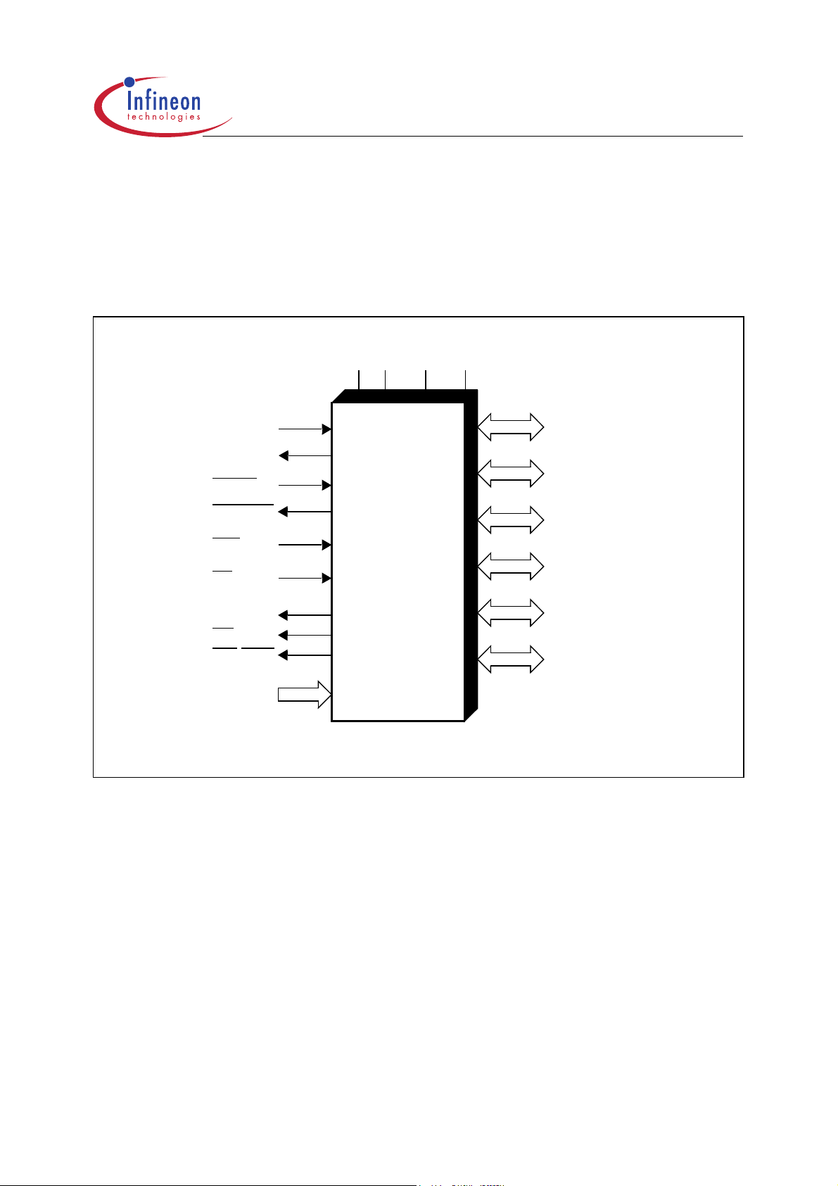
Figure 1 Logic Symbol
Data Sheet 3 1999-07
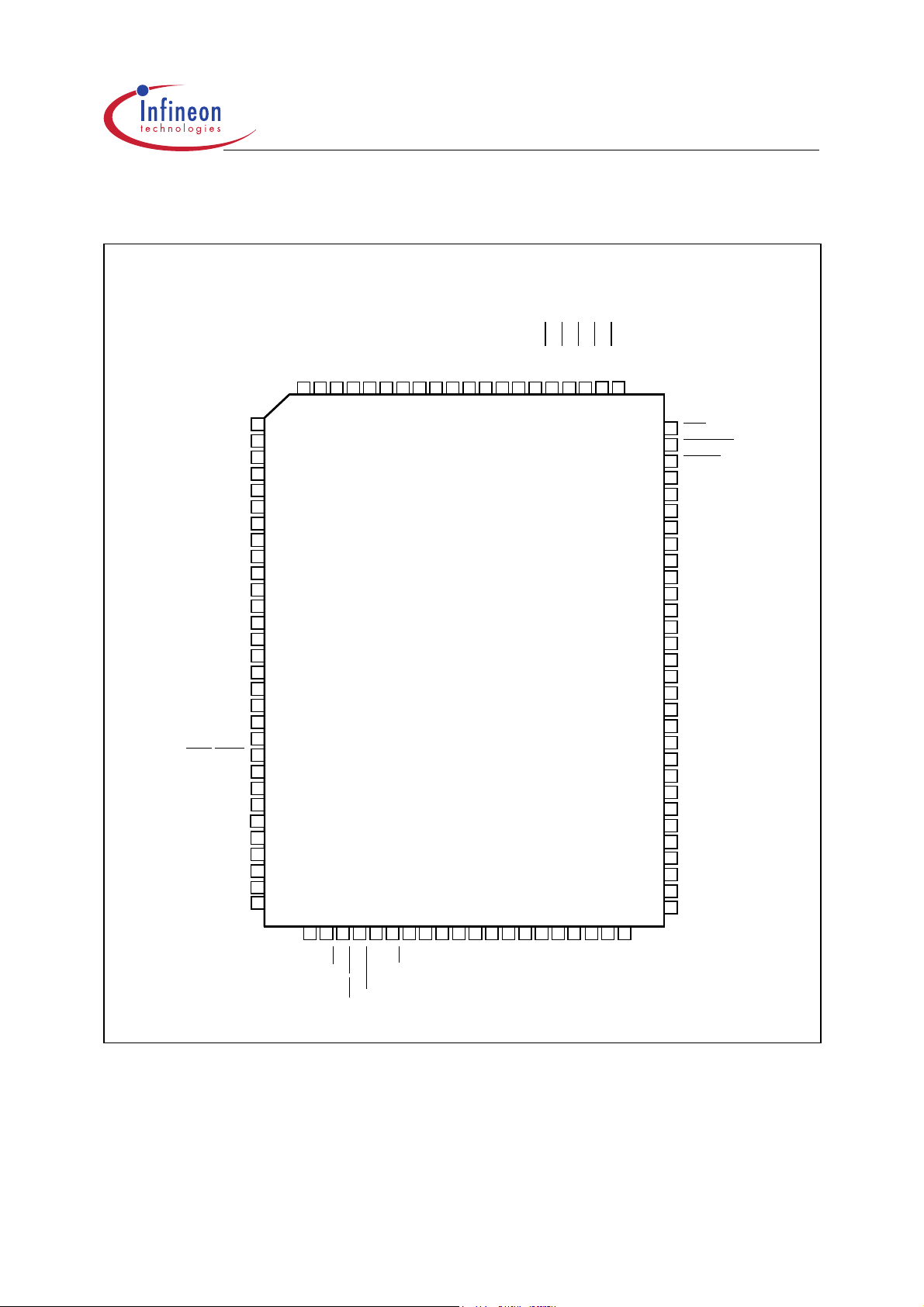
Pin Configuration MQFP Package
(top view)
AGNDVAREF
P5.1/AN1
P5.0/AN0
V
P2.15/EX7IN
&3,
P2.14/EX6IN
P2.13/EX5IN
P2.12/EX4IN
P2.11/EX3IN
P2.10/EX2IN
P2.9/EX1IN
P2.8/EX0IN
P6.7/SDA2
P6.6/SCL1
P6.5/SDA1
P6.4/CS4
P6.3/CS3
P6.2/CS2
P6.1/CS1
P6.0/CS0
P5.2/AN2
P5.3/AN3
P5.14/T4EUD
P5.15/T2EUD
XTAL1
XTAL2
P3.0/SCL0
P3.1/SDA0
P3.2/CAPIN
P3.3/T3OUT
P3.4/T3EUD
P3.5/T4IN
P3.6/T3IN
P3.7/T2IN
P3.8/MRST
P3.9/MTSR
P3.10/TxD0
P3.11/RxD0
P3.12/BHE
/WRH
P3.13/SCLK
P3.15/CLKOUT/
FOUT V
P4.0/A16
P4.1/A17
P4.2/A18
P4.3/A19
P4.4/A20
100999897969594939291908988878685848382
1
2
3
4
V
5
SS
6
7
V
8
DD
9
10
11
12
13
14
C161PI
15
16
17
18
19
20
21
22
23
24
SS
V
25
DD
26
27
28
29
30
31323334353637383940414243444546474849
81
50
80
79
78
77
76
75
74
73
72
71
70
69
68
67
66
65
64
63
62
61
60
59
58
57
56
55
54
53
52
51
NMI
RSTOUT
RSTIN
V
DD
V
SS
P1H.7/A15
P1H.6/A14
P1H.5/A13
P1H.4/A12
P1H.3/A11
P1H.2/A10
P1H.1/A9
P1H.0/A8
V
DD
V
SS
P1L.7/A7
P1L.6/A6
P1L.5/A5
P1L.4/A4
P1L.3/A3
P1L.2/A2
P1L.1/A1
P1L.0/A0
P0H.7/AD15
P0H.6/AD14
P0H.5/AD13
P0H.4/AD12
P0H.3/AD11
P0H.2/AD10
P0H.1/AD9
SS
DD
RD
P4.5/A21
P4.6/A22
WR/WRL
ALE
READY
EA
V
V
P0L.0/AD0
P0L.1/AD1
P0L.2/AD2
P0L.3/AD3
P0L.4/AD4
P0L.5/AD5
SS
DD
V
V
P0L.6/AD6
P0L.7/AD7
P0H.0/AD8
Figure 2
Data Sheet 4 1999-07
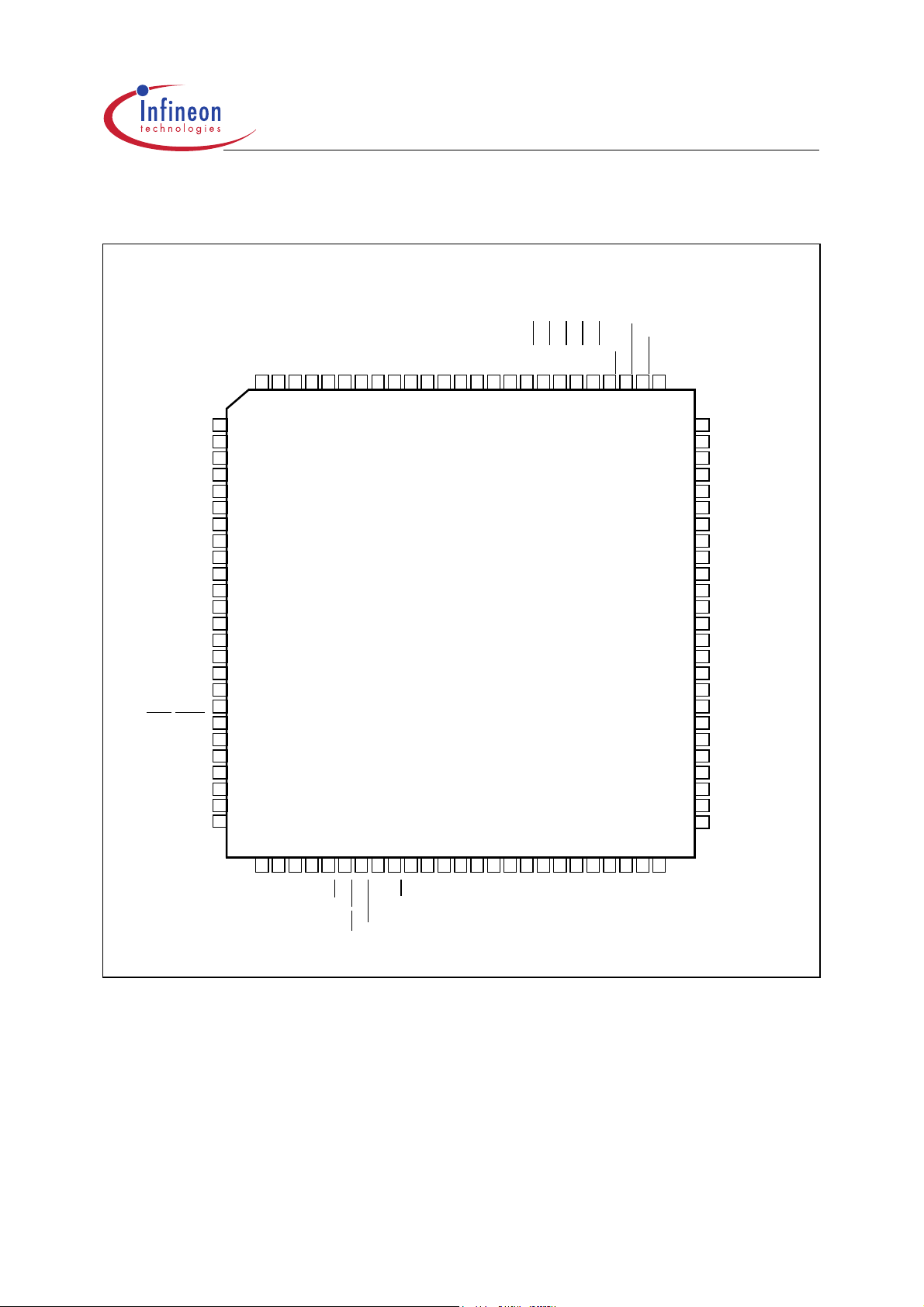
Pin Configuration TQFP Package
(top view)
&3,
P5.14/T4EUD
P5.15/T2EUD
XTAL1
XTAL2
P3.0/SCL0
P3.1/SDA0
P3.2/CAPIN
P3.3/T3OUT
P3.4/T3EUD
P3.5/T4IN
P3.6/T3IN
P3.7/T2IN
P3.8/MRST
P3.9/MTSR
P3.10/TxD0
P3.11/RxD0
P3.12/BHE
/WRH
P3.13/SCLK
P3.15/CLKOUT/
FOUT V
P4.0/A16
P4.1/A17
P5.1/AN1
P5.0/AN0
AGNDVAREF
V
P2.15/EX7IN
P2.14/EX6IN
P2.13/EX5IN
P2.12/EX4IN
P2.11/EX3IN
P2.10/EX2IN
P2.9/EX1IN
P2.8/EX0IN
P6.7/SDA2
P6.6/SCL1
P6.5/SDA1
P6.4/CS4
P6.3/CS3
P6.2/CS2
P6.1/CS1
P6.0/CS0
NMI
RSTOUT
RSTIN
75
V
DD
V
74
SS
73
P1H.7/A15
72
P1H.6/A14
71
P1H.5/A13
70
P1H.4/A12
69
P1H.3/A11
68
P1H.2/A10
67
P1H.1/A9
66
P1H.0/A8
65
V
DD
64
V
C161PI
63
62
61
60
59
58
57
56
55
54
53
52
51
SS
P1L.7/A7
P1L.6/A6
P1L.5/A5
P1L.4/A4
P1L.3/A3
P1L.2/A2
P1L.1/A1
P1L.0/A0
P0H.7/AD15
P0H.6/AD14
P0H.5/AD13
P0H.4/AD12
P0H.3/AD11
P5.3/AN3
P5.2/AN2
100999897969594939291908988878685848382818079787776
1
2
V
3
SS
4
5
V
6
DD
7
8
9
10
11
12
13
14
15
16
17
18
19
20
21
V
23
DD
22
SS
24
25
26272829303132333435363738394041424344454647484950
P4.2/A18
P4.3/A19
P4.4/A20
P4.5/A21
P4.6/A22
RD
WR/WRL
READY
ALE
EA
SS
DD
V
V
P0L.0/AD0
P0L.1/AD1
P0L.2/AD2
P0L.3/AD3
P0L.4/AD4
P0L.5/AD5
P0L.6/AD6
P0L.7/AD7
SS
DD
V
V
P0H.0/AD8
P0H.1/AD9
P0H.2/AD10
Figure 3
Data Sheet 5 1999-07
Table 1 Pin Definitions and Functions
&3,
Symbol Pin
Num.
TQFP
P5
P5.0
P5.1
P5.2
P5.3
P5.14
P5.15
XTAL1
XTAL245
97
98
99
100
1
2
Pin
Num.
MQFP
99
100
1
2
3
4
6
7
Input
Outp.
I
I
I
I
I
I
I
I
O
Function
Port 5 is a 6-bit input-only port with Schmitt-Trigger
characteristics. The pins of Port 5 also serve as (up to
4) analog input channels for the A/D converter, or they
serve as timer inputs:
AN0
AN1
AN2
AN3
T4EUD GPT1 Timer T4 Ext. Up/Down Ctrl. Input
T2EUD GPT1 Timer T5 Ext. Up/Down Ctrl. Input
XTAL1: Input to the oscillator amplifier and input to
the internal clock generator
XTAL2: Output of the oscillator amplifier circuit.
To clock the device from an external source, drive
XTAL1, while leaving XTAL2 unconnected. Minimum
and maximum high/low and rise/fall times specified in
the AC Characteristics must be observed.
Data Sheet 6 1999-07
Table 1 Pin Definitions and Functions (continued)
&3,
Symbol Pin
Num.
TQFP
P3
P3.0
P3.1
P3.2
P3.3
P3.4
P3.5
P3.6
P3.7
P3.8
P3.9
P3.10
P3.11
P3.12
P3.13
P3.15
7
8
9
10
11
12
13
14
15
16
17
18
19
20
21
Pin
Num.
MQFP
9
10
11
12
13
14
15
16
17
18
19
20
21
22
23
Input
Outp.
IO
I/O
I/O
I
O
I
I
I
I
I/O
I/O
O
I/O
O
O
I/O
O
O
Function
Port 3 is a 15 -bit bid irectional I/O port. It is bit-wise
programmable for input or output via direction bits. For
a pin configured as input, the output driver is put into
high-impedance state. Port 3 outputs can be
configured as push/pull or open drain drivers. The input
threshold of Port 3 is selectable (TTL or special). The
following Port 3 pins also serve for alternate functions:
SCL0 I2C Bus Clock Line 0
SDA0 I2C Bus Data Line 0
CAPIN GPT2 Register CAPREL Capture Input
T3OUT GPT1 Timer T3 Toggle Latch Output
T3EUD GPT1 Timer T3 External Up/Down Ctrl.Inp
T4IN GPT1 Timer T4 Count/Gate/Reload/
Capture Input
T3IN GPT1 Timer T3 Count/Gate Input
T2IN GPT1 Timer T2 Count/Gate/Reload/
Capture Input
MRST SSC Master-Rec. / Slave-Trans. Inp/Outp.
MTSR SSC Master-Trans. / Slave-Rec. Outp/Inp.
T×D0 ASC0 Clock/Data Output (Async./Sync.)
R×D0 ASC0 Data Input (Async.) or I/O (Sync.)
BHE
WRH
SCLK SSC Master Clock Outp. / Slave Clock Inp.
CLKOUT System Clock Output (=CPU Clock)
FOUT Programmable Frequency Output
External Memory High Byte Enable Signal,
External Memory High Byte Write Strobe
Note: Pins P3.0 and P3.1 are open drain outputs only.
Data Sheet 7 1999-07
Table 1 Pin Definitions and Functions (continued)
&3,
Symbol Pin
Num.
TQFP
P4
P4.0
P4.1
P4.2
P4.3
P4.4
P4.5
P4.6
RD
24
25
26
27
28
29
30
31 33 O External Memory Read Strobe. RD is activated for
Pin
Num.
MQFP
26
27
28
29
30
31
32
Input
Outp.
IO
O
O
O
O
O
O
O
Function
Port 4 is a 7-bit bidi rectional I/O port. It is bit-wise
programmable for input or output via direction bits. For
a pin configured as input, the output driver is put into
high-impedance state. Port 4 outputs can be
configured as push/pull or open drain drivers. The input
threshold of Port 4 is selectable (TTL or special). Port 4
can be used to output the segment address lines:
A16 Least Significant Segment Addre ss Line
A17 Segment Address Line
A18 Segment Address Line
A19 Segment Address Line
A20 Segment Address Line
A21 Segment Address Line
A22 Most Significant Segment Address Line
every external instruction or data read access.
/
WR
WRL
READY
ALE 34 36 O Address Latch Enable Output. Can be used for latching
32 34 O External Memory Write Strobe. In WR-mode this pin is
activated for every external data write access. In WRL
mode this pin is activated for low byte data write
accesses on a 16-bit bus, and for every data write
access on an 8-bit bus. See WRCFG in register
SYSCON for mode selection.
33 35 I Ready Input. When the Ready function is enabled, a
high level at this pin during an external memory access
will force the insertion of memory cycle time waitstates
until the pin returns to a low level .
An internal pullup device will hold this pin high whe n
nothing is driving it.
the address into externa l memory or a n address latch
in the multiplexed bus modes.
-
Data Sheet 8 1999-07
Table 1 Pin Definitions and Functions (continued)
&3,
Symbol Pin
Num.
TQFP
EA 35 37 I External Access Enable pin. A low level at this pin
PORT0
P0L.0-7
P0H.0-7
3845
4855
Pin
Num.
MQFP
4047
5057
Input
Outp.
IO PORT0 consists of the two 8-bit bidirectional I/O ports
Function
during and after Reset forces the C161PI to begin
instruction execution out of external memory. A high
level forces execution out of the internal program
memory.
"ROMless" versions must have this pin tied to ‘0’.
P0L and P0H. It is bit-wise programmable for input or
output via direction bits. For a pin configured as input,
the output driver is put into high-impedance state.
In case of external bus configurations, PORT0 serves
as the address (A) and address/data (AD) bus in
multiplexed bus modes and as the data (D) bus in
demultiplexed bus modes.
Demultiplexed bus modes:
Data Path Width: 8-bit 16-bit
P0L.0 – P0L.7: D0 – D7 D0 - D7
P0H.0 – P0H.7: I/O D8 - D15
Multiplexed bus modes:
Data Path Width: 8-bit 16-bit
P0L.0 – P0L.7: AD0 – AD7 AD0 - AD7
P0H.0 – P0H.7: A8 - A15 AD8 - AD15
PORT1
P1L.0-7
P1H.0-7
Data Sheet 9 1999-07
5663
6673
5865
6875
IO PORT1 consists of the two 8-bit bidirectional I/O ports
P1L and P1H. It is bit-wise programmable for input or
output via direction bits. For a pin configured as input,
the output driver is put into high-impedance state.
PORT1 is used as the 16-bit address bus (A) in
demultiplexed bus modes and also after switching from
a demultiplexed bus mode to a multiplexed bus mode.
Table 1 Pin Definitions and Functions (continued)
&3,
Symbol Pin
Num.
TQFP
Pin
Num.
MQFP
Input
Outp.
Function
RSTIN 76 78 I/O Reset Input with Schmitt-Trigger characteristics. A low
level at this pin while the oscillator is running resets the
C161PI. An internal pullup resistor permits powe r-on
9
reset using only a capacitor connected to
SS
.
A spike filter suppresses input pulses <10 ns. Input
pulses >100 ns safely pass the filter.
The minimum duration for a safe recognition should be
100 ns + 2 CPU clock cycles.
In bidirectional reset mode (enabled by setting bit
BDRSTEN in register SYSCON) the RSTIN
line is
internally pulled low for th e duration of the internal
reset sequence upon any reset (HW, SW, WDT).
See note below this table.
Note: To let the reset configuration of PORT0 settle
and to let the PLL lock a reset duration of ca.
1 ms is recommended.
RST
OUT
NMI
77 79 O Internal Reset Indication Output. This pin is set to a low
level when the part is executing either a hardware-, a
software- or a watchdog timer reset. RSTOUT
remains
low until the EINIT (end of initialization) instruction is
executed.
78 80 I Non-Maskable Interrupt Input. A high to low transition
at this pin causes the CPU to vector to the NMI trap
routine. When the PWRDN (power down) instruction is
executed, the NMI
C161PI to go into power down mode. If NMI
pin must be low in order to force the
is high,
when PWRDN is executed, the part will continue to run
in normal mode.
If not used, pin NMI
should be pulled high externally.
Data Sheet 10 1999-07
Table 1 Pin Definitions and Functions (continued)
&3,
Symbol Pin
Num.
TQFP
P6
P6.0
P6.1
P6.2
P6.3
P6.4
P6.5
P6.6
P6.7
79
80
81
82
83
84
85
86
P2
P2.8
P2.9
P2.10
P2.11
P2.12
P2.13
P2.14
P2.15
87
88
89
90
91
92
93
94
Pin
Num.
MQFP
81
82
83
84
85
86
87
88
89
90
91
92
93
94
95
96
Input
Outp.
IO
O
O
O
O
O
I/O
I/O
I/O
IO
I
I
I
I
I
I
I
I
Function
Port 6 is an 8 -bit bid irectional I/O port. It is bit-wise
programmable for input or output via direction bits. For
a pin configured as input, the output driver is put into
high-impedance state. Port 6 outputs can be
configured as push/pull or open drain drivers.
The Port 6 pins also serve for alternate functions:
CS0
CS1
CS2
CS3
CS4
SDA1 I
SCL1 I
SDA2 I
Chip Select 0 Output
Chip Select 1 Output
Chip Select 2 Output
Chip Select 3 Output
Chip Select 4 Output
2
C Bus Data Line 1
2
C Bus Clock Line 1
2
C Bus Data Line 2
Note: Pins P6.7-5 are open drain outputs only.
Port 2 is an 8 -bit bid irectional I/O port. It is bit-wise
programmable for input or output via direction bits. For
a pin configured as input, the output driver is put into
high-impedance state. Port 2 outputs can be
configured as push/pull or open drain drivers. The input
threshold of Port 2 is selectable (TTL or special).
The Port 2 pins also serve for alternate functions:
EX0IN Fast External Interrupt 0 Input
EX1IN Fast External Interrupt 1 Input
EX2IN Fast External Interrupt 2 Input
EX3IN Fast External Interrupt 3 Input
EX4IN Fast External Interrupt 4 Input
EX5IN Fast External Interrupt 5 Input
EX6IN Fast External Interrupt 6 Input
EX7IN Fast External Interrupt 7 Input
9
AREF
9
AGND
Data Sheet 11 1999-07
95 97 - Reference voltage for the A/D converter.
96 98 - Reference ground for the A/D converter.
Table 1 Pin Definitions and Functions (continued)
&3,
Symbol Pin
Num.
TQFP
9
DD
6, 23,
37,
47,
65, 75
9
SS
3, 22,
36,
46,
64, 74
Pin
Num.
MQFP
8, 25,
39,
49,
67, 77
5, 24,
38,
48,
66, 76
Input
Function
Outp.
- Digital Supply Voltage:
+ 5 V or + 3 V during normal operati on and idle mode.
≥ 2.5 V during power down mode
- Digital Ground.
Note: The following behaviour differences must be observed when the bidirectional reset
is active:
• Bit BDRSTEN in register SYSCON cannot be changed after EINIT and is cleared
automatically after a reset.
• The reset indication flags always indicat e a long hardware reset.
• The PORT0 configuration is treated like on a hardware reset. Especially the bootstrap
loader may be activated when P0L.4 is lo w.
• Pin RSTIN
may only be connected to external reset devices with an open drain output
driver.
• A short hardware reset is extende d to th e duration of the internal reset sequence.
Data Sheet 12 1999-07
&3,
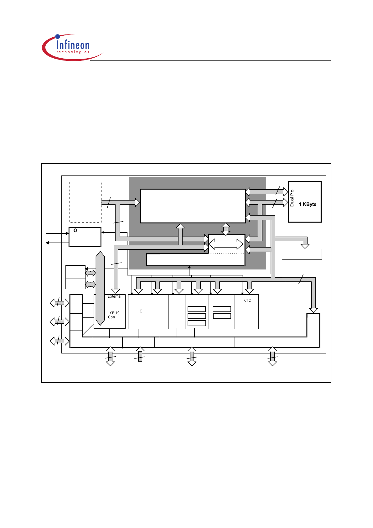
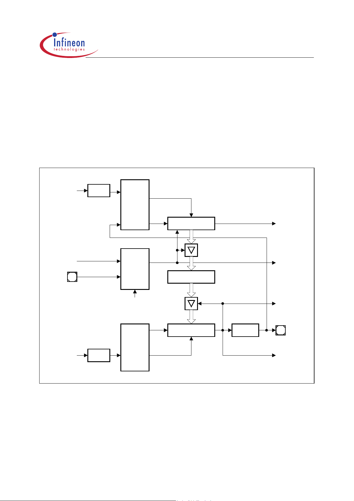
Functional Description
The architecture of the C161PI combines advantages of both RISC and CISC
processors and of advanced p eripheral subsystems in a very well-balanced way. The
following block diagram gives an overview of the different on-chip components and of the
advanced, high bandwidth internal bus structure of the C161PI.
Note: All time specifications refer to a CPU clock of 25 MHz
(see definition in the AC Characteristics section).
XTAL
8
16
7
(no
internal
ROM)
OSC
Oscillator
(input: 16MHz;
(16MHz)
prescaler
PLL
or direct drive)
I²C-Bus
Interface
XRAM
2 KByte
Port 6
Port 0
(16-bit NON MUX Data / Addresses)
XBUS
CS Logic
32
Instr./Data
16
External Instr./Data
16
External
Bus
(MUX
only) &
XBUS
Control,
(4 CS)
16
4-
Channel
10-bit
8-bit
ADC
Port 5
&&RUH
&38&RUH
&38
3(&
Interrupt Controller 11 ext. IR
Interr upt Bus
Peripheral Data
USART
6
ASC
BRG
Sync.
Channel
(SPI)
SSC
BRG
GPT 1
T 2
T 3
T 4
15
GPT 2
T 5
T 6
RTC
Data
Data
16
16
Port 2Port 3Port 4 Port 1
8
Internal
RAM
.%\WH
Dual Port
Watchdog
16
C161RI V0.1
Figure 4 Block Diagram
Data Sheet 13 1999-07

&3,
Memory Organization
The memory space of the C161PI is confi gured in a Von Neumann ar chitecture which
means that code memory, data memory, registers and I/O ports are organized within the
same linear address space which includes 16 MBytes. The entire memory space can be
accessed bytewise or wordwise. Particular portions of the on-chip memory have
additionally been made dire ctly bitaddressable.
1 KByte of on-chip Internal RAM (IRAM) is provided as a storage for user defined
variables, for the system stack, general p urpose register banks and even for code. A
register bank can consist of up to 16 wordwide (R0 to R15) and/or bytewide (RL0, RH0,
…, RL7, RH7) so-called Gene ral P urpose Registers (GPRs).
1024 bytes (2 * 512 bytes) of the a ddress space are reserved for the Special Fun ction
Register areas (SFR space and ESFR space). SFRs are wordwide registers which are
used for controlling and monitoring functions of the different on-chip units. Unused SFR
addresses are reserved for futu re members of the C166 Family.
2 KBytes of on-chip Extension RAM (XRAM) are provided to store user data, user
stacks, or code. The XRAM is accessed like external memory and therefore cannot be
used for the system stack or for register banks and is not bitaddressable. The XRAM
permits 16-bit accesses with maximum speed.
In order to meet the needs of designs wh ere more memory is re quired tha n is pr ovided
on chip, up to 8 MBytes of external RAM and/or ROM can be connected to the
microcontroller.
Data Sheet 14 1999-07

&3,
External Bus Controller
All of the external memory accesses are performed by a particular on-chip External Bus
Controller (EBC). It can be progra mmed either to Single Chip Mode when no external
memory is required, or to one of four different external memory access modes, which are
as follows:
– 16-/18-/20-/23-bit Addresses, 16-bit Data, Demultip lexed
– 16-/18-/20-/23-bit Addresses, 16-bit Data, Multiplexed
– 16-/18-/20-/23-bit Addresses, 8-bit Data, Multiplexed
– 16-/18-/20-/23-bit Addresses, 8-bit Data, Demultiplexed
In the demultiplexed bus mo des, addresses are output on PORT1 and data is input/
output on PORT0 or P0L, respectively. In the multiplexed bus modes both addresses
and data use PORT0 for input/output.
Important timing characteristics of the external bus interface (Memory Cycle Time,
Memory Tri-State Time, Length of ALE and Read Write Delay) have been made
programmable to allow the user the adaption of a wide range of different types of
memories and external peripherals.
In addition, up to 4 independ ent address windows may be defined (via register pairs
ADDRSELx / BUSCONx) which allow to access differe nt resources with different bus
characteristics. These address windows are arrange d hierarchically where BUSCON4
overrides BUSCON3 and BUSCON2 overrides BUSCON1. All accesses to locations not
covered by these 4 address windows are controlled by BUSCON0.
Up to 5 external CS
external glue logic. The C161PI offers the possibility to switch the CS
unlatched mode. In thi s mode the interna l filter log ic is switched off and the CS
are directly generated from the ad dress. The unla tched CS
CSCFG (SYSCON.6).
signals (4 windows plus default) can be generated in order to save
outputs to an
signals
mode is enabled by setting
Access to very slow memories is supported via a particular ‘R eady’ function.
For applications which require less than 8 MBytes of external memory space, this
address space can be restricted to 1 MByte, 256 KByte or to 64 KByte. In this case Port 4
outputs four, two or no address lin es at all. It outputs all 7 address lines, if an address
space of 8 MBytes is used.
Data Sheet 15 1999-07
&3,
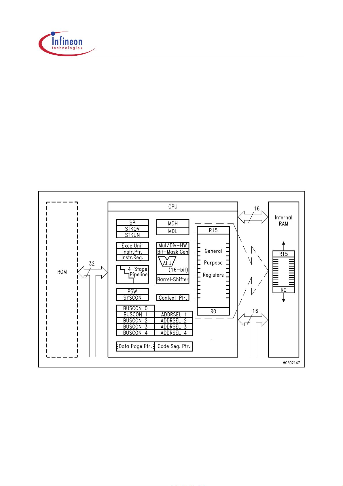
Central Processing Unit (CPU)
The main core of the CP U consists of a 4-stage instru ction pipeline, a 16-bit a rithmetic
and logic unit (ALU) and dedicated SFRs. Additional hardware has been spent for a
separate multiply and divid e unit, a bit-mask generator and a barrel shifter.
Based on these hardware provisions, most of the C161PI’s instructions can be executed
in just one machine cycle which requ ire s 2 CPU clo cks (4 TCL). For example, shift and
rotate instructions are always processed during one machine cycle independent of th e
number of bits to be shifted. All multip le-cycle instructio ns have been o ptimized so that
they can be executed very fast as well: branches in 2 cycles, a 16 × 16 bit multiplication
in 5 cycles and a 32-/16 bit division in 10 cycles. Another pipeline optimization, the so called ‘Jump Cache’, reduces the execution time of repeatedly performed jumps in a loop
from 2 cycles to 1 cycle.
Figure 5 CPU Block Diagram
Data Sheet 16 1999-07

&3,
The CPU has a register context consisting of up to 16 wordwide GPRs at its disposal.
These 16 GPRs are physically allocated within the on-chip RAM area. A Context Pointer
(CP) register determines the base address of the active register bank to be accessed by
the CPU at any time. The number of register banks is only restricted by the avail able
internal RAM space. For easy paramet er passing, a register bank may overlap others.
A system stack of up to 1024 bytes is provided as a storage for temporary data. The
system stack is allocated in the on-chip RAM area, and it is accessed by the CPU via the
stack pointer (SP) register. Two separate SFRs, STKOV and STKUN, are implicitly
compared against the stack pointer value upon each stack access for the detection of a
stack overflow or underflow.
The high performance offered by the hardware implementation of the CPU can efficiently
be utilized by a programmer via the highly efficient C161PI instruction set which includes
the following instruction classes:
– Arithmetic Instructions
– Logical Instructions
– Boolean Bit Manipulation Instructions
– Compare and Loop Control Instru ctio ns
– Shift and Rotate Instructions
– Prioritize Instruction
– Data Movement Instructions
– System Stack Instructions
– Jump and Call Instructions
– Return Instructions
– System Control Instructions
– Miscellaneous Instructions
The basic instruction length is either 2 or 4 bytes. Possible operand types are bits, bytes
and words. A variety of direct, indirect or immediate addressing mo des are provided to
specify the required operand s.
Data Sheet 17 1999-07

&3,
Interrupt System
With an interrupt response time within a range from just 5 to 12 CPU clocks (in case of
internal program execution), the C161PI is capable of reacting very fast to the
occurrence of non-deterministic events.
The architecture of the C161PI supports several mechanisms for fast and flexible
response to service requests th at can be generated from various sources internal or
external to the microcontro ller. Any of these interrupt req uests can be programmed to
being serviced by the Interrupt Controller or by the Peripheral Event Controller (PEC).
In contrast to a standard interrupt service where the current program execution is
suspended and a branch to the interrupt vector table is performed, just one cycle is
‘stolen’ from the current CPU activity to perform a PEC service. A PEC service implies a
single byte or word data transfer betwe en any two memory locations with an additional
increment of either the PEC source or the destination pointer. An individual PEC transfer
counter is implicity decremented for each PEC service except when perfor ming in the
continuous transfer mode. When this counter reaches zero, a standard interrupt is
performed to the correspond ing source related vector lo cation. PEC services are very
well suited, for example, for supporting the transmission or reception of blocks of data.
The C161PI has 8 PEC cha nnels each of which offers such fast interrupt-driven d ata
transfer capabilities.
A separate control re gister which co ntains an interrupt r equ est flag, an in terrupt en able
flag and an interrupt priority bitfield exists for each of the possible interrupt sources. Via
its related register, each source can be progra mmed to one o f sixteen i nterrupt priority
levels. Once having been accepted by the CPU, an interrupt service can only be
interrupted by a higher prioritized service request. For the standard interrupt processing,
each of the possible interrupt sources has a dedicated vector location.
Fast external interrupt inputs are provided to service external interrupts with high
precision requirements. These fast interrupt inputs feature programmable edge
detection (rising edge, falling edge or both edges).
Software interrupts are supported by means of the ‘TRAP’ instruction in combination with
an individual trap (interrupt) number.
The following table shows all of the possible C161PI interrupt sources and the
corresponding hardware-related interrupt flags, vectors, vector locations and trap
(interrupt) numbers.
Note: Interrupt nodes which are not used by associated peripherals, may be used to
generate software controlled interrupt re quests by setting the respective interrupt
request bit (xIR).
Data Sheet 18 1999-07
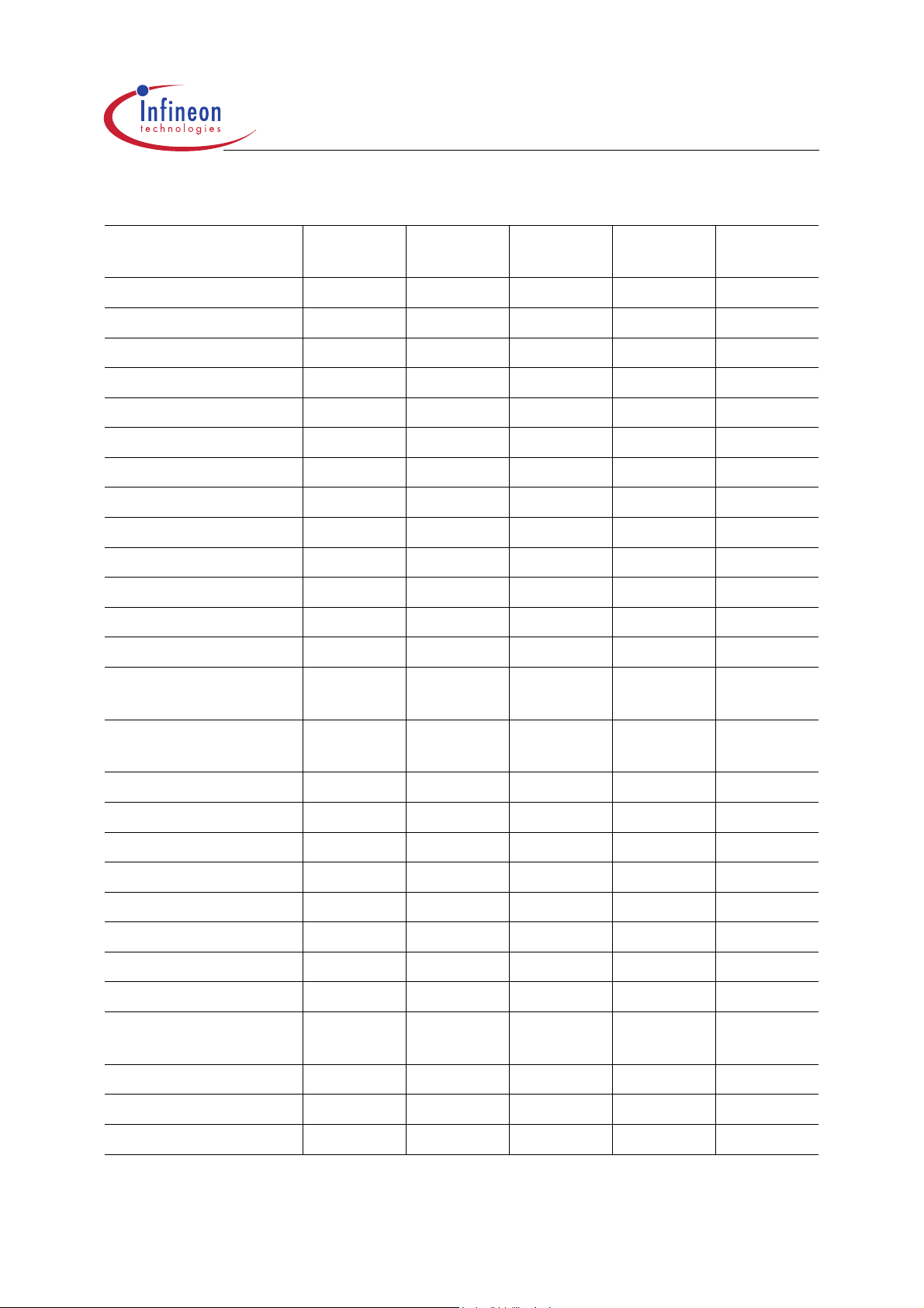
Table 2 C161PI Interrupt Nodes
&3,
Source of Interrupt or
PEC Service Request
Request
Flag
Enable
Flag
Interrupt
Vector
Vector
Location
External Interrupt 0 CC8IR CC8IE CC8INT 00’0060
External Interrupt 1 CC9IR CC9IE CC9INT 00’0064
External Interrupt 2 CC10IR CC10IE CC10INT 00’0068
External Interrupt 3 CC11IR CC11IE CC11INT 00’006C
External Interrupt 4 CC12IR CC12IE CC12INT 00’0070
External Interrupt 5 CC13IR CC13IE CC13INT 00’0074
External Interrupt 6 CC14IR CC14IE CC14INT 00’0078
External Interrupt 7 CC15IR CC15IE CC15INT 00’007C
GPT1 Timer 2 T2IR T2IE T2INT 00’0088
GPT1 Timer 3 T3IR T3IE T3INT 00’008C
GPT1 Timer 4 T4IR T4IE T4INT 00’0090
GPT2 Timer 5 T5IR T5IE T5INT 00’0094
GPT2 Timer 6 T6IR T6IE T6INT 00’0098
GPT2 CAPREL
CRIR CRIE CRINT 00’009C
Register
H
H
H
H
H
H
H
H
H
H
H
H
H
H
Trap
Number
18
H
19
H
1A
H
1B
H
1C
H
1D
H
1E
H
1F
H
22
H
23
H
24
H
25
H
26
H
27
H
A/D Conversion
ADCIR ADCIE ADCINT 00’00A0
28
H
Complete
A/D Overrun Error ADEIR ADEIE ADEINT 00’00A4
ASC0 Transmit S0TIR S0TIE S 0TINT 00’00A8
ASC0 Transmit Buffer S0TBIR S0TBIE S0TBINT 00’011C
29
H
2A
H
47
H
ASC0 Receive S0RIR S0RIE S0RINT 00’00ACH2B
ASC0 Error S0EIR S0EIE S0EINT 00’00B0
SSC Transmit SCTIR SCTIE SCTINT 00’00B4
SSC Receive SCRIR SCRIE SCRINT 00’00B8
2C
H
2D
H
2E
H
SSC Error SCEIR SCEIE SCEINT 00’0 0BCH2F
I2C Data Transfer
XP0IR XP0IE XP0INT 00’0100
40
H
Event
I2C Protocol Event XP1IR XP1IE XP1INT 00’0104
X-Peripheral Node 2 XP2IR XP2IE XP2INT 00’0108
PLL Unlock / RTC XP3IR XP3IE XP3INT 00’010C
41
H
42
H
43
H
H
H
H
H
H
H
H
H
H
H
H
H
H
Data Sheet 19 1999-07
&3,
The C161PI also provides an excellent mechanism to identify and to process exceptions
or error conditions that arise during run-time, so-called ‘Hardware Traps’. Hardware
traps cause immediate non-maskable system reaction which is similar to a standard
interrupt service (branchin g to a dedicated vector ta ble location). The occurence of a
hardware trap is add iti onally signi fie d by a n individ ual bit in the trap fla g register ( TFR).
Except when another higher prio ritized trap service is in progress, a hardware trap will
interrupt any actual program execution. In turn, hardware trap services can normally not
be interrupted by standard or PEC interrupts.
The following table shows all of the possible exceptions or error conditions that can arise
during run-time:
Table 3 Hardware Trap Summary
Exception Condition Trap
Flag
Trap
Vector
Vector
Location
Reset Functions:
Hardware Reset
Software Reset
Watchdog Timer Ov erflow
RESET
RESET
RESET
00’0000
00’0000
00’0000
Class A Hardware Traps:
Non-Maskable Interrupt
Stack Overflow
Stack Underflow
NMI
STKOF
STKUF
NMITRAP
STOTRAP
STUTRAP
00’0008
00’0010
00’0018
Class B Hardware Traps:
Undefined Opco de
Protected Instruction Fault
Illegal Word Operand Access
Illegal Instruction Access
Illegal External Bus Access
UNDOPC
PRTFLT
ILLOPA
ILLINA
ILLBUS
BTRAP
BTRAP
BTRAP
BTRAP
BTRAP
00’0028
00’0028
00’0028
00’0028
00’0028
Reserved [2C
Software Traps:
TRAP Instruction
Any
[00’0000
00’01FC
in steps
of 4
Trap
Number
00
H
H
H
H
H
H
H
H
H
H
H
– 3CH][0BH –
H
00
00
02
04
06
0A
0A
0A
0A
0A
0F
H
H
H
H
H
H
H
Any
–
[00
H
]
H
H
7F
H
H
H
H
H
H
H
]
–
]
Trap
Prio
III
III
III
II
II
II
I
I
I
I
I
Current
CPU
Priority
Data Sheet 20 1999-07

&3,
General Purpose Timer (GPT) Unit
The GPT unit represents a very flexible multifunctional timer/counter structure which
may be used for man y different time related tasks such a s event timing and coun ting,
pulse width and duty cycle measurements, pulse generation, or pulse multiplication.
The GPT unit incorporates five 16-bit timers which are organized in two separate
modules, GPT1 and GPT2. Each timer in each module may operate indep endently in a
number of different modes, or may be concatenated with another timer of the same
module.
Each of the three timers T2, T3, T4 of module GPT1 can be configured individually for
one of four basic modes of operation, which are Timer, Gated Timer, Counter, and
Incremental Interface Mode. In Time r Mode, the input clock for a timer is derived from
the CPU clock, divided by a programmable prescaler, while Counter Mode allows a timer
to be clocked in reference to external events.
Pulse width or duty cycle measurement is supported in Gated Timer Mode, where the
operation of a timer is controlled by the ‘gate’ leve l on an external input pin. For these
purposes, each timer has one associated port pin (TxIN) which serves as gate or clock
input. The maximum resolution of the timers in module GPT1 is 16 TCL.
The count direction (up/down) for each timer is programmable by software or may
additionally be altered dynamically by an external signal on a port pin (TxEUD) to
facilitate eg. position tracking.
In Incremental Interface Mo de the GPT1 timers (T2, T3 , T4) can be directly con nected
to the incremental position sensor signals A and B via their respective inputs TxIN and
TxEUD. Direction and count signals are intern ally derived from these two input sign als,
so the contents of the respective timer Tx corresponds to the sensor position. The third
position sensor signal TOP0 can be connected to an interrupt inpu t.
Timer T3 has an output toggle latch (T3OTL) which changes its state on each timer overflow/underflow. The state of this latch may be output on a port pin (T3OUT) eg. for time
out monitoring of external hardware components, or may be used internally to clock
timers T2 and T4 for measuring long time per iods with high resolution.
In addition to their basic operating modes, timers T2 and T4 may be configured as reload
or capture registers for timer T3. When used as capture or reload registers, timers T2
and T4 are stopped. The contents of timer T3 are captured into T2 or T4 in response to
a signal at their asso ciated input p ins (TxIN). Timer T3 is reloa ded with the contents of
T2 or T4 triggered either by an e xternal signa l or by a se lectable state tra nsition of its
toggle latch T3OTL. When both T2 and T4 are configured to al ternately reload T3 on
opposite state transi tions of T3OTL with the low and hi gh times of a PWM signal, this
signal can be constantly generated without software intervention.
Data Sheet 21 1999-07
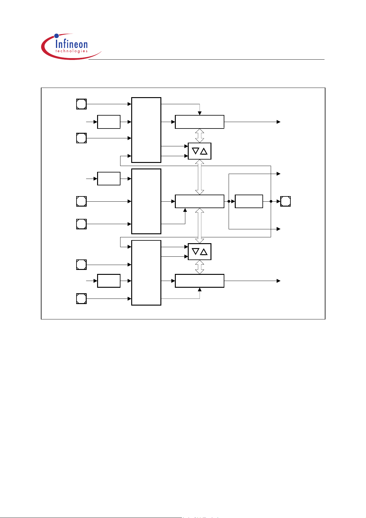
&3,
T2EUD
T2IN
T3IN
T3EUD
T4IN
f
f
f
CPU
CPU
CPU
2n : 1
2n : 1
2n : 1
T2
Mode
Control
T3
Mode
Control
T4
Mode
Control
U/D
GPT1 Timer T2
Reload
Capture
GPT1 Timer T3 T3OTL
U/D
Capture
Reload
GPT1 Timer T4
Interrupt
Request
Interrupt
Request
Toggle FF
T3OUT
Other
Timers
Interrupt
Request
T4EUD
U/D
MCT02141
Figure 6 Block Diagram of GPT1
With its maximum resolution of 8 TCL, the GPT2 module provides precise event control
and time measurement. It includes two timers (T5, T6) and a capture/reload register
(CAPREL). Both timers can be clocked with an input clock which is derived from the CPU
clock via a programmable prescaler. The count direction (up/down) for each timer is
programmable by software. Concatenation of the timers is supported via the output
toggle latch (T6OTL) of timer T6, which changes its state on each timer overflow/
underflow.
Data Sheet 22 1999-07
&3,
The state of this latch may be used to clock ti mer T5. The overflows/underflows of timer
T6 can additionally be used to cause a reload from the CAPREL register. The CAPREL
register may capture the contents of timer T5 based on an external sig nal tr ansition on
the corresponding port pin (CAPIN), and timer T5 may optionally b e cleared after the
capture procedure. This allows absolute time differences to be measured or pulse
multiplication to be performed without software overhead.
The capture trigger (ti mer T5 to CAPREL) may also be gen erated upon transitions of
GPT1 timer T3’s inputs T3IN and/or T3EUD. This is especially advantageous when T3
operates in Incremental Interface Mode.
CAPIN
f
CPU
f
CPU
T3
2n : 1
2n : 1
T5
Mode
Control
MUX
CT3
T6
Mode
Control
GPT2 Timer T5
Clear
Capture
GPT2 CAPREL
GPT2 Timer T6
U/D
U/D
T6OTL
Interrupt
Request
Interrupt
Request
Interrupt
Request
T6OUT
Other
Timers
Mcb03999C.vsd
Figure 7 Block Diagram of GPT2
Data Sheet 23 1999-07

&3,
Real Time Clock
The Real Time Clock (RTC) module of the C161PI consists of a chain of 3 divider blocks,
a fixed 8:1 divider, the reloadable 16-bit timer T14, and the 32-bit RTC timer (accessible
via registers RTCH and RTCL). The RTC module is directly clocked with the on-chip
I
oscillator frequency divided by 32 via a separate clock driver (
RTC
= I
therefore independent from the selected clock generation mode of the C161PI. All timers
count up.
The RTC module can be used for different purposes:
• System clock to determine the current time and date
• Cyclic time based interrupt
• 48-bit timer for long term measurements
/ 32) and is
OSC
T14REL
Reload
f
T14
8:1
RTCLRTCL
RTC
Interrupt
Request
Figure 8 RTC Block Diagram
Note: The registers associated with the RTC are not effected by a reset in order to
maintain the correct system time even when intermediate resets are executed.
Data Sheet 24 1999-07

&3,
A/D Converter
For analog signal measurement, a 10-bit A/D converter with 4 multiplexed input channels
and a sample and hold circuit has been integrated on-chip. It uses the method of
successive approximation. The sample time (for loading the capacitors) and the
conversion time is programmab le and can so be adjusted to the external circuitry.
Overrun error detection/protection is provided for the conversion result register
(ADDAT): either an interrup t request will be generated when the result of a previous
conversion has not been read from the result reg iste r at the time the ne xt conver si on is
complete, or the next conversion is susp ended in such a ca se until the previo us result
has been read.
For applications which require less than 4 analog input channels, the remaining channel
inputs can be used as digital input port pins.
The A/D converter of the C161PI supports four different conversion modes. In the
standard Single Chann el conversion mode, the analog level on a specified channel is
sampled once and converted to a digital result. In the Single Channel Continuous mode,
the analog level on a specified channel is repeatedly sa mpled and converted without
software intervention. In the Auto Scan mode, the analog levels on a prespecified
number of channels are sequentially sampled and converted. In the Auto Scan
Continuous mode, the number of prespecified channels is repeatedly sampled and
converted. In addition, the conversion of a specific channel can be inserted (injected) into
a running sequence witho ut disturbing this sequence. This is called Channel Injection
Mode.
The Peripheral Event Controller (PEC) may be used to automatically store the
conversion results into a table in memory for later evaluation, without requiring the
overhead of entering and exiting interrupt routines for each data transfer.
After each reset and also during normal operation the ADC automatically performs
calibration cycles. This automatic self-calibration constantly adjusts the converter to
changing operating conditions (e.g. te mperature) and compensates process variation s.
These calibration cycles are part of the conversion cycle, so they do not affect the normal
operation of the A/D converter.
In order to decouple an alog inputs from digital noise and to avoid input trigger noise
those pins used for analog input can be disconnected from the digital IO or input stages
under software control. This can be selected for each pin separately via registers
P5DIDIS (Port 5 Digital Input Disable).
Data Sheet 25 1999-07

&3,
Serial Channels
Serial communication with other microcontrollers, processors, terminals or external
peripheral components is provided by two serial interfaces with different functionality, an
Asynchronous/Synchronous Serial Channel (ASC0) and a High-Speed Synchronous
Serial Channel (SSC).
The ASC0 is upward compatible with the serial ports of the Infineon 8-bit microcontroller
families and supports full-duplex asynchronous communication at up to 780 KBaud and
half-duplex synchronous communication at up to 3.1 MBaud @ 25 MHz CPU clock.
A dedicated baud rate generator allows to set up all standard baud rates without
oscillator tuning. For transmission, reception and error handling 4 separate interrupt
vectors are provided. In asynchrono us mode, 8- or 9-bit data frames are transmitted or
received, preceded by a start bit and terminated by one or two stop bits. For
multiprocessor communication, a mechanism to distinguish address from data bytes has
been included (8-bit data plu s wake up bit mode).
In synchronous mode, the ASC0 transmits or receives bytes (8 bits) synchronously to a
shift clock which is generated by the ASC0. The ASC0 always shifts the LSB first. A loop
back option is available for testing purposes.
A number of optional hardware error detection capabilities has been included to increase
the reliability of data transfers. A parity bit can automatically be generated on
transmission or be checked on reception. Framing er ror detection allows to recognize
data frames with missing stop bits. An overrun error will be generated, if the last
character received has not been read out of the receive buffer register at the time the
reception of a new character is complete.
The SSC supports full-duplex synchronous communication at up to 6.25 Mbaud @
25 MHz CPU clock. It may be config ured so it interfaces with serially linked perip heral
components. A dedicated baud rate gen erator allows to set up all standard baud rates
without oscillator tuning. For transmission, reception and error handling 3 separate
interrupt vectors are provided.
The SSC transmits or receives characters of 2...16 bits length synchronously to a shift
clock which can be generated by the SSC (master mode) or by an external master (slave
mode). The SSC can start shifting with the LSB or with the MSB and allows the selection
of shifting and latching clock edges as well as the clock polarity.
A number of optional hardware error detection capabilities has been included to increase
the reliability of data transfers. Transmit and receive error supervise the correct handling
of the data buffer. Phase and baudrate error detect incorrect serial data.
Data Sheet 26 1999-07

&3,
I2C Module
2
The integrated I
the two-line I
can receive and transmit data using 7-bit or 10-bit addressing and it can operate in slave
mode, in master mode or in multi-master mode.
Several physical interfaces (port pi ns) can be established un der software control. Data
can be transferred at speeds up to 400 Kbit/sec.
Two interrupt nodes dedicated to the I
support operation via PEC transfers.
C Bus Module handles the tra nsmission and rece ption of frames ove r
2
C bus in accordance with the I2C Bus specification. The on-chip I2C Module
2
C module allow efficient interrupt service and also
Note: The port pins associated with the I2C interfaces feature open drain drivers only, as
2
required by the I
C specification.
Watchdog Timer
The Watchdog Timer represents one of the fail-safe mechanisms which have been
implemented to prevent the controller from malfunctioning for longer periods of time.
The Watchdog Timer is always enabled after a reset of the chip, and can only be
disabled in the time interval until th e EINIT (end of initialization) instruction has been
executed. Thus, the chip’s start-up procedure is always monitored. The software has to
be designed to service the Watchdog Timer b efore it overflows. If, due to hardware or
software related failures, the software fails to do so, the Watchdog Timer overflows and
generates an internal hardware reset and pulls the RSTOUT
pin low in order to allow
external hardware components to be reset.
The Watchdog Timer is a 16-bit timer, clocked with the system clock divided either by 2
or by 128. The high byte of th e Watchdog Timer register can be set to a prespecified
reload value (stored in WDTREL) in order to allow further variation of the monitored time
interval. Each time it is serviced by the application software, the high byte of the
Watchdog Timer is reloaded. Thus, time inte rvals between 20 µs and 336 ms can be
monitored (@ 25 MHz).
The default Watchdog Timer interval after reset is 5.24 ms (@ 25 MHz).
Data Sheet 27 1999-07

&3,
Parallel Ports
The C161PI provides up to 7 6 IO lines which are organized in to six input/output ports
and one input port. All port lines are bit-addressable, and all input/output lines are
individually (bit-wise) programmable as inputs or outputs via direction registers. The I/O
ports are true bidirectional ports which are switched to high impedance state when
configured as inputs. The output drivers of three IO ports can be configured (pin by pin)
for push/pull operation o r open-dra in operation via control r egisters. The oth er IO ports
operate in push/pull mode, except fo r the I²C interface pins which are open drain pins
only. During the internal reset, all port pin s are configured as inputs.
All port lines have programmable alternate input or output functions associated with
them. All port lines that are not used for these alternate functions may be used as general
purpose IO lines.
PORT0 and PORT1 may be used as ad dress and data lines when accessing external
memory, while Port 4 outputs the additional segment a ddress bits A22/19/17...A16 in
systems where segmentation is enabled to access more than 64 KBytes of memory.
Port 3 includes alternate function s of timers, serial interfaces, the optional bus control
signal BHE
and the system clock output CLKOUT (or the programmable frequency
output FOUT).
Port 5 is used for the analog input channels to the A/D converter or timer control signals.
Port 6 provides the optional chip select signals and interfa ce lines for the I²C module.
The edge characteristics (transitio n time) of the C161PI’s port drivers can be selecte d
via the Port Driver Control Register (PDCR).
Data Sheet 28 1999-07

&3,
Instruction Set Summary
The table below lists the instructions of the C161PI in a condensed way.
The various addressing modes that can be used with a specific instruction, the operation
of the instructions, parameters for conditional execution of instructions, and the opcodes
for each instruction can be found in the “C166 Family Instruction Set Manual”.
This document also provides a deta illed description of each instruction.
Table 4 Instruction Set Summary
Mnemonic Description Bytes
ADD(B) Add word (byte) operands 2 / 4
ADDC(B) Add word (byte) operands with Carry 2 / 4
SUB(B) Subtract word (byte) operands 2 / 4
SUBC(B) Subtract word (byte) operands with Carry 2 / 4
MUL(U) (Un)Signed multiply direct GPR by direct GPR (16-16-bit) 2
DIV(U) (Un)Signed divide register MDL by direct GPR (16-/16-bit) 2
DIVL(U) (Un)Signed long divide reg. MD by direct GPR (32-/16-bit) 2
CPL(B) Complement direct word (byte) GPR 2
NEG(B) Negate direct word (byte) GPR 2
AND(B) Bitwise AND, (word/byte operands) 2 / 4
OR(B) Bitwise OR, (word/byte operands) 2 / 4
XOR(B) Bitwise XOR, (word/byte operands) 2 / 4
BCLR Clear direct bit 2
BSET Set direct bit 2
BMOV(N) Move (negated) direct bit to direct bit 4
BAND, BOR,
BXOR
BCMP Compare direct bit to direct bit 4
BFLDH/L Bitwise modify masked high/low byte of bit-addressable
CMP(B) Compare word (byte) operands 2 / 4
CMPD1/2 Compare word data to GPR and decrement GPR by 1/2 2 / 4
AND/OR/XOR direct bit with direct bit 4
4
direct word memory with immediate data
CMPI1/2 Compare word data to GPR and increment GPR by 1/2 2 / 4
PRIOR Determine number of shift cycles to no rmalize direct
word GPR and store result in direct word GPR
SHL / SHR Shift left/right direct word GPR 2
ROL / ROR Rotate left/right direct word GPR 2
ASHR Ar ithmetic (sign bit) shift right direct word GPR 2
Data Sheet 29 1999-07
2

&3,
Table 4 Instruction Set Summary (continued)
Mnemonic Description Bytes
MOV(B) Move word (byte) data 2 / 4
MOVBS Move byte operand to word operand with sign exte nsion 2 / 4
MOVBZ Move byte operand to word operand. with zero extension 2 / 4
JMPA, JMPI,
JMPR
JMPS Jump absolute to a code segment 4
J(N)B Jump relative if direct bit is (not) set 4
JBC Jump relative and clear bit if direct bit is set 4
JNBS Jump relative and set bit if direct bit is not set 4
CALLA, CALLI,
CALLR
CALLS Call absolute subroutine in any code segme nt 4
PCALL Push direct word register onto system stack and call
TRAP Call interrupt service routine via immediate trap number 2
PUSH, POP Push/pop direct word reg iste r onto/from system stack 2
SCXT Push direct word register onto system stack und update
RET Return from intra-segment subroutine 2
RETS Return from inter-segment subroutine 2
RETP Return from intra-segment subroutine and pop direct
Jump absolute/indirect/relative if condition is met 4
Call absolute/indirect/relative subroutine if condition is met 4
absolute subroutine
register with word operand
word register from system stack
4
4
2
RETI Return from interrupt service subroutine 2
SRST Software Reset 4
IDLE Enter Idle Mode 4
PWRDN Enter Power Down Mode (supposes NMI
SRVWDT Service Watchdog Timer 4
DISWDT Disable Watchdog Timer 4
EINIT Signify End-of- Initialization on RSTOUT-pin 4
ATOMIC Begin ATOMIC sequence 2
EXTR Begin EXTend ed Register sequence 2
EXTP(R) Begin EXTended Pa ge (and Register) sequence 2 / 4
EXTS(R) Begin EXTended Segme nt (and Register) sequence 2 / 4
NOP Null operation 2
Data Sheet 30 1999-07
-pin being low) 4

&3,
Special Function Registers Overview
The following table lists all SFRs which are implemented in the C161PI in alpha betical
order.
Bit-addressable SFRs are marked with the letter “b” in column “Name”. SFRs within the
Extended SFR-Space (ESFRs) are marked with the letter “E” in column “Physical
Address”. Registers within on-chip X- Peripherals (I²C) are marked with th e letter “X” in
column “Physical Address”.
An SFR can be specified via its individual mnemonic na me. Depending on the selected
addressing mode, an SFR can be a ccessed via its physical address (using the Da ta
Page Pointers), or via its short 8-bit address (witho ut us ing the Data Page Pointers).
Table 5 C161PI Registers, Ordered by Name
Name Physical
Address
ADCIC b FF98
ADCON b FFA0
ADDAT FEA0
ADDAT2 F0A0
ADDRSEL1 FE18
ADDRSEL2 FE1A
ADDRSEL3 FE1C
ADDRSEL4 FE1E
ADEIC b FF9A
BUSCON0 b FF0C
BUSCON1 b FF14
BUSCON2 b FF16
BUSCON3 b FF18
BUSCON4 b FF1A
CAPREL FE4A
CC8IC b FF88
CC9IC b FF8A
CC10IC b FF8C
CC11IC b FF8E
H
H
H
H
H
H
H
H
H
H
H
H
H
H
H
H
H
H
H
8-Bit
Addr.
CC
D0
50
E 50
0C
0D
0E
0F
CD
86
8A
8B
8C
8D
25
C4
C5
C6
C7
Description Reset
A/D Converter End of Conversion
H
Interrupt Control Register
A/D Converter Control Register 0000
H
A/D Converter Result Register 0000
H
A/D Converter 2 Result Register 0000
H
Address Select Register 1 0000
H
Address Select Register 2 0000
H
Address Select Register 3 0000
H
Address Select Register 4 0000
H
A/D Converter Overrun Error Interrupt
H
Control Register
Bus Configuration Register 0 0000
H
Bus Configuration Register 1 0000
H
Bus Configuration Register 2 0000
H
Bus Configuration Register 3 0000
H
Bus Configuration Register 4 0000
H
GPT2 Capture/Reload Register 0000
H
External Interrupt 0 Control Register 0000
H
External Interrupt 1 Control Register 0000
H
External Interrupt 2 Control Register 0000
H
External Interrupt 3 Control Register 0000
H
Value
0000
0000
H
H
H
H
H
H
H
H
H
H
H
H
H
H
H
H
H
H
H
Data Sheet 31 1999-07

Table 5 C161PI Registers, Ordered by Name (continued)
&3,
Name Physical
Address
CC12IC b FF90
CC13IC b FF92
CC14IC b FF94
CC15IC b FF96
CP FE10
CRIC b FF6A
CSP FE08
DP0L b F100
DP0H b F102
DP1L b F104
DP1H b F106
DP2 b FFC2
DP3 b FFC6
DP4 b FFCA
DP6 b FFCE
DPP0 FE00
H
H
H
H
H
H
H
H
H
H
H
H
H
H
H
H
8-Bit
Addr.
C8
C9
CA
CB
08
B5
04
E 80
E 81
E 82
E 83
E1
E3
E5
E7
00
Description Reset
External Interrupt 4 Control Reg ister 0000
H
External Interrupt 5 Control Reg ister 0000
H
External Interrupt 6 Control Reg ister 0000
H
External Interrupt 7 Control Reg ister 0000
H
CPU Context Pointer Re gister FC00
H
GPT2 CAPREL Interrupt Ctrl. Register 0000
H
CPU Code Segment Pointer Regi ster
H
(8 bits, not directly writeable)
P0L Direction Control Register 00
H
P0H Direction Control Register 00
H
P1L Direction Control Register 00
H
P1H Direction Control Register 00
H
Port 2 Direction Control Register 0000
H
Port 3 Direction Control Register 0000
H
Port 4 Direction Control Register 00
H
Port 6 Direction Control Register 00
H
CPU Data Page Pointer 0 Registe r (10
H
bits)
Value
0000
0000
H
H
H
H
H
H
H
H
H
H
H
H
H
H
H
H
DPP1 FE02
DPP2 FE04
DPP3 FE06
EXICON b F1C0
H
H
H
H
ICADR ED06HX --- I²C Address Register 0XXX
ICCFG ED00HX --- I²C Configuration Register XX00
ICCON ED02HX --- I²C Contro l Register 0000
ICRTB ED08HX --- I²C Receive/Transmit Buffer XX
ICST ED04HX --- I²C Status Reg ister 0000
IDCHIP F07C
IDMANUF F07E
IDMEM F07A
H
H
H
01
02
03
E E0
E 3E
E 3F
E 3D
CPU Data Page Pointer 1 Reg. (10 bits) 0001
H
CPU Data Page Pointer 2 Reg. (10 bits) 0002
H
CPU Data Page Pointer 3 Reg. (10 bits) 0003
H
External Interrupt Control Registe r 0000
H
Identifier 09XX
H
Identifier 1820
H
Identifier 0000
H
H
H
H
H
H
H
H
H
H
H
H
H
Data Sheet 32 1999-07

Table 5 C161PI Registers, Ordered by Name (continued)
&3,
Name Physical
Address
IDPROG F078
H
8-Bit
Addr.
E 3C
ISNC b F1DEHE EF
MDC b FF0E
MDH FE0C
MDL FE0E
H
H
H
87
06
07
ODP2 b F1C2HE E1
ODP3 b F1C6HE E3
ODP6 b F1CEHE E7
ONES b FF1E
P0L b FF00
P0H b FF02
P1L b FF04
P1H b FF06
P2 b FFC0
P3 b FFC4
P4 b FFC8
P5 b FFA2
P5DIDIS b FFA4
P6 b FFCC
PECC0 FEC0
PECC1 FEC2
PECC2 FEC4
PECC3 FEC6
PECC4 FEC8
PECC5 FECA
PECC6 FECC
PECC7 FECE
PSW b FF10
H
H
H
H
H
H
H
H
H
H
H
H
H
H
H
H
H
H
H
H
8F
80
81
82
83
E0
E2
E4
D1
D2
E6
60
61
62
63
64
65
66
67
88
PDCR F0AAHE 55
RP0H b F108
H
E 84
Description Reset
Identifier 0000
H
Interrupt Subnode Control Registe r 0000
H
CPU Multiply Divide Control Register 0000
H
CPU Multiply Divide Reg. – High Word 0000
H
CPU Multiply Divide Reg. – Low Word 0000
H
Port 2 Open Drain Control Register 0000
H
Port 3 Open Drain Control Register 0000
H
Port 6 Open Drain Control Register 00
H
Constant Value 1’s Register (read only) FFFF
H
Port 0 Low Reg. (Lower half of PORT0) 00
H
Port 0 High Reg. (Upper half of PORT0) 00
H
Port 1 Low Reg. (Lower half of PORT1) 00
H
Port 1 High Reg. (Upper half of PORT1) 00
H
Port 2 Register 0000
H
Port 3 Register 0000
H
Port 4 Register (7 bits) 00
H
Port 5 Register (read only) XXXX
H
Port 5 Digital Input Disable Register 0000
H
Port 6 Register (8 bits) 00
H
PEC Channel 0 Control Register 0000
H
PEC Channel 1 Control Register 0000
H
PEC Channel 2 Control Register 0000
H
PEC Channel 3 Control Register 0000
H
PEC Channel 4 Control Register 0000
H
PEC Channel 5 Control Register 0000
H
PEC Channel 6 Control Register 0000
H
PEC Channel 7 Control Register 0000
H
CPU Program Status Word 0000
H
Pin Driver Control Register 0000
H
System Startup Config. Reg. (Rd. only) XX
H
Value
H
H
H
H
H
H
H
H
H
H
H
H
H
H
H
H
H
H
H
H
H
H
H
H
H
H
H
H
H
H
Data Sheet 33 1999-07

Table 5 C161PI Registers, Ordered by Name (continued)
&3,
Name Physical
Address
RTCH F0D6
RTCL F0D4
S0BG FEB4
S0CON b FFB0
S0EIC b FF70
S0RBUF FEB2
S0RIC b FF6E
S0TBIC b F19C
S0TBUF FEB0
H
H
H
H
H
H
H
H
H
8-Bit
Addr.
E 6B
E 6A
5A
D8
B8
59
B7
E CE
58
Description Reset
RTC High Register no
H
RTC Low Register no
H
Serial Channel 0 Bau d Rate Generator
H
Reload Register
Serial Channel 0 Control Register 0000
H
Serial Channel 0 Error Interrupt Control
H
Register
Serial Channel 0 Receive Buffer Reg.
H
(read only)
Serial Channel 0 Receive Interrupt
H
Control Register
Serial Channel 0 Transmit Buffer
H
Interrupt Control Register
Serial Channel 0 Transmit Buffer Reg.
H
(write only)
Value
0000
0000
XXXX
0000
0000
0000
H
H
H
H
H
H
H
S0TIC b FF6C
SP FE12
SSCBR F0B4
SSCCON b FFB2
SSCEIC b FF76
SSCRB F0B2
SSCRIC b FF74
SSCTB F0B0
SSCTIC b FF72
STKOV FE14
STKUN FE16
SYSCON b FF12
SYSCON2 b F1D0
SYSCON3 b F1D4
T14 F0D2
H
H
H
H
H
H
H
H
H
H
H
H
H
H
H
B6
09
E 5A
D9
BB
E 59
BA
E 58
B9
0A
0B
89
E E8
E EA
E 69
Serial Channel 0 Transmit Interrupt
H
Control Register
CPU System Stack Pointer Register FC00
H
SSC Baudrate Register 0000
H
SSC Control Register 0000
H
SSC Error Interrupt Control Register 0000
H
SSC Receive Buffer XXXX
H
SSC Receive Interrupt Control Register 0 000
H
SSC Transmit Buffer 0000
H
SSC Transmit Interrupt Control Register 0000
H
CPU Stack Overflow Pointer Register FA00
H
CPU Stack Underflow P ointer Register FC00
H
CPU System Configuration Register
H
CPU System Configuration Register 2 0000
H
CPU System Configuration Register 3 0000
H
RTC Timer 14 Register no
H
0000
1)
0xx0
H
H
H
H
H
H
H
H
H
H
H
H
H
H
Data Sheet 34 1999-07

Table 5 C161PI Registers, Ordered by Name (continued)
&3,
Name Physical
Address
T14REL F0D0HE 68
T2 FE40
T2CON b FF40
T2IC b FF60
T3 FE42
T3CON b FF42
T3IC b FF62
T4 FE44
T4CON b FF44
T4IC b FF64
T5 FE46
T5CON b FF46
T5IC b FF66
T6 FE48
T6CON b FF48
T6IC b FF68
TFR b FFAC
WDT FEAE
WDTCON FFAE
XP0IC b F186
XP1IC b F18E
XP2IC b F196
XP3IC b F19E
ZEROS b FF1C
1) The system configuration is selected during reset.
2) The reset value depends on the indicated reset source.
H
H
H
H
H
H
H
H
H
H
H
H
H
H
H
H
H
H
H
H
H
H
H
8-Bit
Addr.
20
A0
B0
21
A1
B1
22
A2
B2
23
A3
B3
24
A4
B4
D6
57
D7
E C3
E C7
E CB
E CF
8E
Description Reset
RTC Timer 14 Reload Register no
H
GPT1 Timer 2 Register 0000
H
GPT1 Timer 2 Control Register 0000
H
GPT1 Timer 2 Interrupt Control Register 0000
H
GPT1 Timer 3 Register 0000
H
GPT1 Timer 3 Control Register 0000
H
GPT1 Timer 3 Interrupt Control Register 0000
H
GPT1 Timer 4 Register 0000
H
GPT1 Timer 4 Control Register 0000
H
GPT1 Timer 4 Interrupt Control Register 0000
H
GPT2 Timer 5 Register 0000
H
GPT2 Timer 5 Control Register 0000
H
GPT2 Timer 5 Interrupt Control Register 0000
H
GPT2 Timer 6 Register 0000
H
GPT2 Timer 6 Control Register 0000
H
GPT2 Timer 6 Interrupt Control Register 0000
H
Trap Flag Register 0000
H
Watchdog Timer Register (read only) 0000
H
Watchdog Timer Control Register
H
I²C Data Interrupt Control Register 0000
H
I²C Protocol Interrupt Control Register 0000
H
X-Peripheral 2 Interrupt Control Register 0000
H
RTC Interrupt Control Register 0000
H
Constant Value 0’s Register (read only) 0000
H
Value
2)
00xx
H
H
H
H
H
H
H
H
H
H
H
H
H
H
H
H
H
H
H
H
H
H
H
Data Sheet 35 1999-07

Absolute Maximum Ratings
Table 6 Absolute Maximum Rating Parameters
Parameter Symbol Limit Values Unit Notes
min. max.
&3,
Storage temperature
9
Voltage on
respect to ground (
pins with
DD
9
SS
)
Voltage on any pin with
9
respect to ground (
SS
)
Input current on any pin
7
9
9
ST
DD
IN
-65 150 °C
-0.5 6.5 V
-0.5 9DD+0.5 V
-10 10 mA
during overload condition
Absolute sum of all input
- |100| mA
currents during overload
condition
Power dissipation
3
DISS
1.5 W
Note: Stresses above those listed under “Absolute Maximum Ratings” may cause
permanent damage to the device. This is a stress rating only and functional
operation of the device at these or any othe r conditions abo ve those ind icated in
the operational sections of this specification is not implied . Exposure to absol ute
maximum rating conditions for extended periods may affect device reliability.
9
>
9
or
9
<
9
During absolute maximum rating overload conditions (
9
voltage on
pins with respect to ground (
DD
9
) must not exceed the values
SS
IN
DD
IN
SS
) the
defined by the absolute maximum ratings.
Data Sheet 36 1999-07

&3,
Operating Conditions
The following operating conditions must not be exceeded in order to ensure correct
operation of the C161PI. All parameters specified in the following sections refer to these
operating conditions, unless otherwise no ticed.
Table 7 Operating Condition Parameters
Parameter Symbol Limit Values Unit Notes
min. max.
Standard
digital supply voltage
Reduced
digital supply voltage
Digital ground voltage
Overload current
Absolute sum of overload
currents
External Load
Capacitance
9
9
9
,
DD
DD
SS
OV
4.5 5.5 V Active mode,
2.5
1)
5.5 V PowerDown mo de
3.0 3.6 V Active mode,
2.5
1)
3.6 V PowerDown mo de
0 V Reference voltage
- ±5 mA Per pin 2)
Σ|,OV|- 50 mA
&
L
- 100 pF Pin drivers in
- 50 pF Pin drivers in
I
CPUmax
I
CPUmax
3)
= 25 MHz
= 20 MHz
3)
fast edge mode
(PDCR.BIPEC =
’0’)
reduced edge
mode
(PDCR.BIPEC =
3)
’1’)
Ambient temperature 7
A
0 7 0 °C SAB-C161PI...
-40 85 °C SAF-C161PI...
-40 125 °C SAK-C161PI...
1) Output voltages and output currents will be reduced when 9DD leaves the range defined for active mode.
2) Overload conditio ns occur if the standard operatings conditions are exceeded, i.e. the voltage on any pin
9
! 9
exceeds the specified range (i.e.
currents on all port pins may not exceed 50 mA. The supply voltage must remain within the specified limits.
3) Not 100% tested, guaranteed by design characterization.
Data Sheet 37 1999-07
OV
+0.5V or 9
DD
OV
9
-0.5V). The absolute sum of input overload
SS

&3,
Parameter Interpretation
The parameters listed in the following partly represent the characteristics of the C161PI
and partly its demands on th e system. To aid in interpreting the parameters right, when
evaluating them for a design, they are marked in column “Symbol”:
CC (Controller Characteristics):
The logic of the C161PI will provide signals with the respe ctive timing characteristics.
SR (System Requirement):
The external system must provide signals with the respective timing ch aracteristics to
the C161PI.
DC Characteristics (Standard Supply Voltage Range)
(Operating Condition s apply)
Parameter Symbol Limit Values Unit Test Condition
Input low voltage XTAL1,
P3.0, P3.1, P6.5, P6.6, P6.7
Input low voltage
(TTL)
Input low voltage
(Special Threshold)
Input high voltage RSTIN
Input high voltage XTAL1,
P3.0, P3.1, P6.5, P6.6, P6.7
Input high voltage
(TTL)
Input high voltage
(Special Threshold)
Input Hysteresis
(Special Threshold)
min. max.
9
SR – 0.5 0.3
IL1
9
SR – 0.5 0.2 9
IL
V
DD
DD
V–
V–
– 0.1
9
SR – 0.5 2.0 V –
ILS
9
SR 0.6 9
IH1
DD9DD
+
V–
0.5
9
SR 0.7 9
IH2
DD9DD
+
V–
0.5
9
9
IH
IHS
SR 0.2 9
+ 0.9
SR 0.8 9
- 0.2
DD
DD
9
DD
0.5
9
DD
0.5
+
+
V–
V–
HYS 400 – mV –
9
Output low voltage
CC – 0.45 V ,OL = 2.4 mA
OL
(PORT0, PORT1, Port 4, ALE,
, WR, BHE, CLKOUT,
RD
RSTOUT
Output low voltage
)
9
CC – 0.4 V ,
OL2
= 3 mA
OL2
(P3.0, P3.1, P6.5, P6.6, P6.7)
Data Sheet 38 1999-07

&3,
DC Characteristics (Standard Supply Voltage Range) (continued)
(Operating Conditions apply)
Parameter Symbol Limit Values Unit Test Condition
min. max.
Output low voltage
(all other outputs)
Output high voltage
1)
(PORT0, PORT1, Port 4, ALE,
, WR, BHE, CLKOUT,
RD
RSTOUT
Output high voltage
)
1)
(all other outputs)
Input leakage current (Port 5)
Input leakage current (all other) ,
RSTIN inactive current
RSTIN active current
Read/Write inactive current
Read/Write active current
ALE inactive current
ALE active current
Port 6 inactive current
Port 6 active current
PORT0 configuration current
2)
2)
5)
5)
5)
5)
5)
5)
5)
XTAL1 input current ,
Pin capacitance
6)
(digital inputs/outputs)
Power supply current (5V active)
with all peripherals active
Idle mode supply current (5V)
with all peripherals active
Idle mode supply current (5V)
with all peripherals deactivated,
PLL off, SDD factor = 32
9
CC –0.45V,OL = 1.6 mA
OL1
9
CC 2.4 – V ,OH = -2.4 mA
OH
9
0.9
9
CC 2.4 – V ,OH = -1.6 mA
OH1
0.9
,
CC – ±200 nA 0.45V < 9IN < 9
OZ1
CC – ±500 nA 0.45V < 9IN < 9
OZ2
,
,
,
,
,
,
,
,
,
,
&
,
,
,
3)
RSTH
RSTL
RWH
RWL
ALEL
ALEH
P6H
P6L
P0H
P0L
IL
IO
DD5
IDX5
IDO5
–-10µA 9IN = 9
4)
-100 – µA 9IN = 9
3)
–-40µA 9
4)
-500 – µA 9
3)
–40µA 9
4)
500 – µA 9
3)
–-40µA 9
4)
-500 – µA 9
3)
–-10µA 9IN = 9
4)
-100 – µA 9IN = 9
CC – ±20 µA0 V < 9IN < 9
CC – 10 pF I = 1 MHz
–1 +
–1 +
8)
– 500 +
–V,OH = -0.5 mA
DD
9
–V,OH = -0.5 mA
DD
OUT
OUT
OUT
OUT
OUT
OUT
7
= 25 °C
A
mA RSTIN = 9
2*
I
CPU
I
CPU
mA RSTIN = 9
0.8*
I
CPU
I
CPU
µA RSTIN = 9
50*
I
OSC
I
OSC
IH1
IL
= 2.4 V
= 9
OLmax
= 9
OLmax
= 2.4 V
= 2.4 V
= 9
OL1max
IHmin
ILmax
IL2
in [MHz]
IH1
in [MHz]
IH1
in [MHz]
DD
DD
DD
7)
7)
7)
Data Sheet 39 1999-07

&3,
DC Characteristics (Standard Supply Voltage Range) (conti nued)
(Operating Condition s apply)
Parameter Symbol Limit Values Unit Test Condition
min. max.
Power-down mode supply
,
current (5V) with RTC running
Power-down mode supply
,
current (5V) with RTC disabled
1) This specification is not valid for outputs which are switched to open drain mode. In this case the respective
output will float and the voltage results from the external circuitry.
2) These parameters describe the RSTIN
3) The maximum current may be drawn while the respective signal line remains inactive.
4) The minimum current must be drawn in order to drive the respective signal line active.
5) This specification is only valid during Reset, or during Hold- or Adapt-mode. During Hold mode Port 6 pins are
only affected, if they are used (configured) for CS
6) Not 100% tested, guaranteed by design characterization.
7) The supply current is a function of the operating frequency. This dependency is illustrated in the figure below.
These parameters are tested at
9
or 9IH.
at
IL
The oscillator also contributes to the total supply current. The given values refer to the worst case, ie. I
For lower oscillator frequencies the respective supply current can be reduced accordingly.
8) This parameter is determined mainly by the current consumed by the oscillator. This current, however, is
influenced by the external oscillator circuitry (crystal, capacitors). The values given refer to a typical circuitry
and may change in case of a not optimized external oscillator circuitry.
9) This parameter is tested including leakage currents. All inputs (including pins configured as inputs) at 0 V to
9
0.1 V or at
– 0.1 V to 9DD, 9
DD
pullup, which equals a resistance of ca. 50 to 250 KΩ.
9
and maximum CPU clock with all outputs disconnected and all inputs
DDmax
= 0 V, all outputs (including pins configured as outputs) disconnected.
REF
PDR5
PDO5
8)
–200 +
I
25*
–50µA
output and the open drain function is not enabled.
OSC
µA
9
DD
I
OSC
9
DD
=
=
in [MHz]
9
DDmax
9
DDmax
9)
9)
PDRmax
.
Data Sheet 40 1999-07

&3,
DC Characteristics (Reduced Supply Voltage Range)
(Operating Conditions apply)
Parameter Symbol Limit Values Unit Test Condition
min. max.
9
Input low voltage XTAL1,
P3.0, P3.1, P6.5, P6.6, P6.7
Input low voltage
(TTL)
Input low voltage
(Special Threshold)
Input high voltage RSTIN
Input high voltage XTAL1,
P3.0, P3.1, P6.5, P6.6, P6.7
SR – 0.5 0.3
IL1
9
SR – 0.5 0.8 V –
IL
9
SR – 0.5 1.3 V –
ILS
9
SR 0.6 9
9
IH1
IH2
SR 0.7 9
DD9DD
DD9DD
0.5
0.5
V
+
+
DD
V–
V–
V–
Input high voltage
(TTL)
Input high voltage
(Special Threshold)
Input Hysteresis
(Special Threshold)
Output low voltage
(PORT0, PORT1, Port 4, ALE,
, WR, BHE, CLKOUT,
RD
RSTOUT
)
Output low voltage
P3.0, P3.1, P6.5, P6.6, P6.7
Output low voltage
(all other outputs)
Output high voltage
1)
(PORT0, PORT1, Port 4, ALE,
, WR, BHE, CLKOUT,
RD
RSTOUT
Output high voltage
)
1)
(all other outputs)
9
SR 1.8 9DD +
IH
V–
0.5
9
SR 0.8 9
IHS
- 0.2
DD
9
DD
0.5
+
V–
HYS 250 – mV –
9
CC – 0.45 V ,OL = 1.6 mA
OL
9
CC – 0.4 V ,
OL2
9
CC – 0.45 V ,OL = 1.0 mA
OL1
9
CC 0.9 9DD –V,OH = -0.5 mA
OH
9
CC 0.9 9DD –V,OH = -0.25 mA
OH1
OL2
= 1.6 mA
,
Input leakage current (Port 5)
Input leakage current (all other) ,
RSTIN inactive current
Data Sheet 41 1999-07
2)
CC – ±200 nA 0.45V < 9IN < 9
OZ1
CC – ±500 nA 0.45V < 9IN < 9
OZ2
RSTH
3)
–-10µA 9IN = 9
,
DD
DD
IH1

&3,
DC Characteristics (continued) (Reduced Supply Voltage Range)
(Operating Condition s apply)
Parameter Symbol Limit Values Unit Test Condition
min. max.
RSTIN active current
Read/Write inactive current
Read/Write active current
ALE inactive current
ALE active current
Port 6 inactive current
Port 6 active current
PORT0 configuration current
2)
5)
5)
5)
5)
5)
5)
5)
XTAL1 input current ,
Pin capacitance
6)
(digital inputs/outputs)
Power supply current (3V active)
with all peripherals active
Idle mode supply current (3V)
with all peripherals active
Idle mode supply current (3V)
with all peripherals deactivated,
PLL off, SDD factor = 32
Power-down mode supply
current (3V) with RTC running
Power-down mode supply
current (3V) with RTC disabled
1) This specification is not valid for outputs which are switched to open drain mode. In this case the respective
output will float and the voltage results from the external circuitry.
2) These parameters describe the RSTIN
3) The maximum current may be drawn while the respective signal line remains inactive.
4) The minimum current must be drawn in order to drive the respective signal line active.
5) This specification is only valid during Reset, or during Hold- or Adapt-mode. During Hold mode Port 6 pins are
only affected, if they are used (configured) for CS
6) Not 100% tested, guaranteed by design characterization.
pullup, which equals a resistance of ca. 50 to 250 KΩ.
4)
,
RSTL
,
RWH
,
RWL
,
ALEL
,
ALEH
,
P6H
,
P6L
,
P0H
,
P0L
IL
&
IO
,
DD3
,
IDX3
,
IDO3
,
PDR3
,
PDO3
-100 – µA 9IN = 9
3)
– -10 µA 9
4)
-500 – µA 9
3)
–20µA 9
4)
500 – µA 9
3)
– -10 µA 9
4)
-500 – µA 9
3)
–-5µA 9IN = 9
4)
-100 – µA 9IN = 9
OUT
OUT
OUT
OUT
OUT
OUT
CC – ±20 µA0 V < 9IN < 9
CC – 10 pF I = 1 MHz
7
A
–1 +
1.1*
–1 +
0.5*
8)
–300 +
30*
8)
–100 +
10*
I
I
mA RSTIN = 9
I
CPU
mA RSTIN =
I
CPU
µARSTIN = 9
OSC
µA 9DD = 9
OSC
I
CPU
I
CPU
I
OSC
I
OSC
–30µA 9DD = 9
output and the open drain function is not enabled.
IL
= 2.4 V
= 9
OLmax
= 9
OLmax
= 2.4 V
= 2.4 V
= 9
OL1max
IHmin
ILmax
= 25 °C
in [MHz]
in [MHz]
in [MHz]
DDmax
in [MHz]
DDmax
DD
IL2
7)
9
IH1
7)
IH1
7)
9)
9)
Data Sheet 42 1999-07

&3,
7) The supply current is a function of the operating frequency. This dependency is illustrated in the figure below.
9
These parameters are tested at
9
or 9IH.
at
IL
The oscillator also contributes to the total supply current. The given values refer to the worst case, ie. I
For lower oscillator frequencies the respective supply current can be reduced accordingly.
8) This parame ter is determined mainly by the current consumed by the oscillator. This current, however, is
influenced by the external oscillator circuitry (crystal, capacitors). The values given refer to a typical circuitry
and may change in case of a not optimized external oscillator circuitry.
9) This paramet er is tested including leakage currents. All inputs (including pi ns configured as inputs) at 0 V t o
9
0.1 V or at
– 0.1 V to 9DD, 9
DD
I [µA]
and maximum CPU clock with all outputs disconnected and all inputs
DDmax
= 0 V, all outputs (including pins configured as outputs) disconnected.
REF
PDRmax
.
1500
,
,'2PD[
1250
1000
,
,'2PD[
750
,
3'5PD[
500
,
3'5PD[
250
,
3'2PD[
I
[MHz]
4
8 12 16
OSC
Figure 9 Idle and Power Down Supply Current as a Function of Oscillator
Frequency
Data Sheet 43 1999-07

&3,
50
25
, [mA]
I
DD3max
I
DD3typ
I
DD5max
I
DD5typ
I
ID5max
I
ID5typ
I
ID3max
I
ID3typ
5
5 10 15 25
20
I
CPU
[MHz]
Figure 10 Supply/Idle Current as a Function of Operating Frequency
Data Sheet 44 1999-07

AC Characteristics
Definition of Internal Timing
&3,
The internal operati on of the C161PI is cont rolled by the intern al CPU clock f
CPU
. Both
edges of the CPU clock can trigger inte rnal (e.g. pipeline) or external (e.g. bus cycles)
operations.
The specification of the externa l timing (AC Characteristics) therefore depends on the
time between two consecutive edges of the CPU clock, called “TCL” (see figure below).
3KDVH/RFNHG/RRS2SHUDWLRQ
I
26&
I
&38
TCLTCL
'LUHFW&ORFN'ULYH
I
26&
I
&38
TCLTCL
3UHVFDOHU2SHUDWLRQ
I
26&
I
&38
TCL TCL
Figure 11 Generation Mechanisms for the CPU Clock
The CPU clock signal
can be generated from the oscillator clock signal I
CPU
OSC
via
I
different mechanisms. The duration of TCLs and their variation (a nd also the derived
I
external timing) depends o n the used mechanism to generate
. This influence must
CPU
be regarded when calculating the timings fo r the C161PI.
Note: The example for PLL operation shown in the fig. above refers to a PLL factor of 4.
The used mechanism to generate the CPU cl ock is selected during reset via the logic
levels on pins P0.15-13 (P0H.7-5).
The table below associates the combinations of these three bits with the respective clock
generation mode.
Data Sheet 45 1999-07

Table 8 C161PI Clock Generation Modes
&3,
P0.15-13
(P0H.7-5)
11 1
110
101
100
011
010 I
001
000
1) The external clock input range refers to a CPU clock range of 10...25 MHz.
2) The maximum frequency depends on the duty cycle of the external clock signal.
CPU Frequency
I
CPU
= I
I
I
I
I
I
OSC
I
OSC
* F
OSC
* 4 2.5 to 6.25 MHz Default configuration
OSC
* 3 3.33 to 8.33 MHz
OSC
* 2 5 to 12.5 MHz
OSC
* 5 2 to 5 MHz
OSC
* 1 1 to 25 MHz Direct drive
OSC
* 1.5 6.66 to 16.6 MHz
I
/ 2 2 to 50 MHz CPU clock via prescaler
OSC
* 2.5 4 to 10 MHz
External Clock
Input Range
1)
Notes
2)
Prescaler Operation
When pins P0.15-13 (P0H.7- 5) equal 001
during reset the CPU clock is derived from
B
the internal oscillator (input clock signal) by a 2:1 pre scaler.
I
The frequency of
is half the frequency of I
CPU
the duration of an individual TCL) is defined by the period of the input clock
and the high and low time of I
OSC
I
OSC
CPU
.
(i.e.
The timings listed in the AC Characteristics that refer to TCLs therefore can be
I
calculated using the per iod of
for any TCL.
OSC
Phase Locked Loop
For all combinations of pins P0.15 -13 (P0H.7-5) except fo r 001
and 011B the on-chip
B
phase locked loop is enabled and provides the CPU clock ( see table above). The PL L
multiplies the input frequency b y the factor F which is selected via the combination of
pins P0.15-13 (i.e.
CPU
= I
* F). With every F’th transition of I
OSC
the PLL circuit
OSC
I
synchronizes the CPU clock to th e input clock. This synchroniza tion is done smoothly,
i.e. the CPU clock frequency does not change abruptly.
I
Due to this adaptation to the input clock the frequency of
I
it is locked to
. The slight variation causes a jitter of I
OSC
is constantly adjusted so
CPU
which also effects the
CPU
duration of individual TCLs.
Data Sheet 46 1999-07

&3,
The timings listed in the AC Characteristics that refer to TCLs therefore must be
calculated using the minimum TCL that is possible under the respective circumstances.
The actual minimum value for TCL depends on the jitter of the PLL. As the PLL is
constantly adjusting its output frequency so it corresponds to the applied input frequency
(crystal or oscillator) the relative deviation for periods of more than one TCL is lower than
for one single TCL (see formula and figure below).
N
For a period of
deviation D
where
:
N
N
* TCL)
(
N
= number of consecutive TCLs and 1 ≤ N ≤ 40.
So for a period of 3 TCLs @ 25 MHz (i.e.
and (3TCL)
min
This is especially important for bus cycles using waitsta tes and e.g. fo r the op era tion of
timers, serial interfaces, etc. For all slower operations and longer periods (e.g. pulse train
generation or measurement, lower baudrates, etc.) the deviation caused by the PLL jitter
is neglectible.
* TCL the minimum value is computed using the corresponding
= N * TCL
min
= 3TCL
- 1.288 ns = 58.7 ns (@ I
NOM
NOM
- D
N
DN [ns] = ±(13.3 + N*6.3) / I
N
= 3): D3 = (13.3 + 3 * 6.3) / 25 = 1.288 ns,
= 25 MHz).
CPU
CPU
[MHz],
Note: For all periods longer than 40 TCL the N=40 value can be used (see figure below).
±26.5
±
20
±
10
±1
Max.jitter D1 [ns]
This approximated formula is valid for
1 ≤ 1 ≤ 40 and 10MHz ≤ f
≤ 25MHz.
CPU
40201051
10 MHz
16 MHz
20 MHz
25 MHz
N
Figure 12 Approximated Maximum Accumulated PLL Jitter
Data Sheet 47 1999-07

Direct Drive
&3,
When pins P0.15-13 (P0H.7-5) equal 011
during reset the on-chip phase locked loop is
B
disabled and the CPU clock is directly driven from the internal oscillator with the in put
clock signal.
I
The frequency of
I
(i.e. the duration of an individual TCL) is defined by the duty cycle of the input clock
CPU
I
.
OSC
directly follows the frequency of I
CPU
so the high and low time of
OSC
The timings listed below that refer to TCLs therefore must be calculated using the
minimum TCL that is possible under the respective circumstances. This minimum value
can be calculated via the following formula:
min
= 1/I
TCL
For two consecutive TCLs the deviation caused by the duty cycle of
so the duration of 2TCL is always 1/
OSC
* DC
min
(DC = duty cycle)
I
. The minimum value TCL
OSC
I
is compensated
OSC
therefore has to be
min
used only once for timings that req uire an odd number of TCLs (1,3,...). Timings that
I
require an even number of TCLs (2,4,...) may use the formula 2TCL = 1/
Note: The address float timings in Multiple xed bus mode (
= 1/
I
duration of TCL (TCL
max
OSC
* DC
) instead of TCL
max
W
11
and
min
W
) use the maximum
45
.
OSC
.
Data Sheet 48 1999-07

AC Characteristics
External Clock Drive XTAL1 (Standard Supply Voltage Range)
(Operating Conditions apply)
&3,
Parameter Symbol Direct Drive
1:1
Prescaler
2:1
PLL
1:N
Unit
min. max. min. max. min. max.
W
Oscillator period
High time
Low time
Rise time
Fall time
1) The minimum and maximum oscillator periods for PLL operation depend on the selected CPU clock generation
mode. Please see respective table above.
2) The clock input signal must reach the defined levels
3) The min imum high and low time refers to a duty cycle of 50%. The maximu m operating frequency (I
direct drive mode depends on the duty cycle of the clock input signal.
2)
2)
2)
2)
SR 40 – 20 – 60
OSC
W
SR 20
1
W
SR 20
2
W
SR–10–6–10ns
3
W
SR–10–6–10ns
4
3)
–6–10–ns
3)
–6–10–ns
and
9
IL
.
9
IH2
1)
500
1)
ns
) in
CPU
AC Characteristics
External Clock Drive XTAL1 (Reduced Supply Voltage Range)
(Operating Conditions apply)
Parameter Symbol Direct Drive
1:1
Prescaler
2:1
PLL
1:N
Unit
min. max. min. max. min. max.
W
Oscillator period
High time
Low time
Rise time
Fall time
1) The minimum and maximum oscillator periods for PLL operation depend on the selected CPU clock generation
mode. Please see respective table above.
2) The clock input signal must reach the defined levels 9
3) The min imum high and low time refers to a duty cycle of 50%. The maximu m operating frequency (I
direct drive mode depends on the duty cycle of the clock input signal.
2)
2)
2)
2)
SR 50 – 25 – 60
OSC
W
SR 25
1
W
SR 25
2
W
SR–10–6–10ns
3
W
SR–10–6–10ns
4
3)
–8–10–ns
3)
–8–10–ns
and 9
IL
IH2
.
1)
Data Sheet 49 1999-07
500
1)
ns
) in
CPU

Figure 13 External Clock Drive XTAL1
&3,
Note: The main oscillator is optimized for oscilla tion with a crystal within a frequency
range of 4...16 MHz. When driven by an external clock signal it will accept the
specified frequency range. Operation at lower input frequencies is possible but is
guaranteed by design only (not 100% tested).
It is strongly recommended to measure the oscillation allowance (or margin) in the
final target system (layout) to determine the optimum parameters for the oscillator
operation.
Data Sheet 50 1999-07

&3,
A/D Converter Characteristics
(Operating Conditions apply)
9
4.0V (2.6V)≤
9
- 0.1V ≤ 9
SS
Parameter Symbol Limit Values Unit Test Condition
Analog input voltage range
Basic clock frequency I
Conversion time W
Total unadjusted error TUE CC
Internal resistance of
reference voltage source
Internal resistance of analog
source
ADC input capacitance &
1) 9
may exceed 9
AIN
cases will be X000
2) The limit values for I
3) This parameter includes the sample time WS, the time for determining the digital result and the time to load the
result register with the conversion result.
Values for the basic clock
This parameter depends on the ADC control logic. It is not a real maximum value, but rather a fixum.
4) TUE is tested at 9
voltages within the defined voltage range.
The specified TUE is guaranteed only if an overload condition (see
selected analog input pins and the absolute sum of input overload currents on all analog input pins does not
exceed 10 mA.
During the reset calibration sequence the maximum TUE may be ±4 LSB (±8 LSB @ 3V).
5) This case is not applicable for the reduced supply voltage range.
6) During the conversion the ADC’s capacitance must be repeatedly charged or discharged. The internal
resistance of the reference voltage source must allow the capacitance to reach its respective voltage level
within each conversion step. The maximum internal resistance results from t he programmed conversion timing.
7) Not 100% tested, guaranteed by design.
8) During the sample time the input capacitance &I can be charged/discharged by the external source. The
internal resistance of the analog source must allow the capacitance to reach its final voltage level within
After the end of the sample time
Values for the sample time
≤ 9DD + 0.1V (Note the influence on TUE.)
AREF
≤ 9SS + 0.2V
AGND
min. max.
9
SR 9
AIN
BC
CC –40 WBC +
C
AGND
0.5 6.25 MHz
– ± 2 LSB 9
4)
– ± 4 LSB 9
5
5
or 9
AGND
or X3FFH, respectively.
H
must not be exceeded when selecting the CPU frequency and the ADCTC setting.
BC
=5.0V (3.3V),
AREF
up to the absolute maximum ratings. However, the conversion result in these
AREF
W
depend on the conversion time programming.
BC
W
, changes of the analog input voltage have no effect on the conversion result.
S
W
depend on programming and can be taken from the table below.
S
SR – WBC / 60
AREF
SR – WS / 450
ASRC
CC – 33 pF
AIN
9
=0V, 9DD=4.9V (3.2V). It is guaranteed by design for all other
AGND
9
W
S
AREF
+2W
V
CPU
1)
2)
3)
W
CPU
= 1 / I
AREF
AREF
≥ 4.0 V
≥ 2.6 V
kΩ WBC in [ns]
- 0.25
kΩ WS in [ns]
- 0.25
7)
,
specification) occurs on maximum 2 not
OV
CPU
5)
6) 7)
7) 8)
W
.
S
Data Sheet 51 1999-07

&3,
Sample time and conversion time of the C161PI’s A/D Converter are programmable. The
table below should be used to calculate the above timings.
The limit values for
I
must not be exceeded when selecting ADCTC.
BC
Table 9 A/D Converter Computation Table
ADCON.15|14
(ADCTC)
00
01
10
11
A/D Converter
Basic clock
I
/ 4 00 WBC * 8
CPU
I
/ 2 01 WBC * 16
CPU
I
/ 16 10 WBC * 32
CPU
I
/ 8 11 WBC * 64
CPU
Converter Timing Exam ple:
Assumptions:
Basic clock
Sample time
Conversion time
I
CPU
I
BC
W
S
W
C
ADCON.13|12
I
BC
= 25 MHz (i.e. W
= I
/ 4 = 6.25 MHz, i.e. WBC = 160 ns.
CPU
(ADSTC)
CPU
= WBC * 8 = 1280 ns.
= WS + 40 WBC + 2 W
CPU
Sample time
W
S
= 40 ns), ADCTC = ’00’, ADSTC = ’00’.
= (1280 + 6400 + 80) ns = 7.8 µs.
Memory Cycle Variables
The timing tables below use three variables which are derived from the BUSCONx
registers and represen t the special characteristics of the programmed memory cycle.
The following table describes, how these variables are to be computed.
Table 10 Memory Cycle Variables
Description Symbol Values
ALE Extension
Memory Cycle Time Waitstates
Memory Tristate Time
Data Sheet 52 1999-07
W
A
W
C
W
F
TCL * <ALECTL>
2TCL * (15 - <MCTC>)
2TCL * (1 - <MTTC>)

Testing Waveforms
&3,
2.4 V
1.8 V 1.8 V
Test Points
0.45 V
AC inputs during testing are driven at 2.4 V for a logic ‘1’ and 0.45 V for a logic ‘0’.
Timing measurements are made at
0.8 V 0.8 V
9
min for a logic ’1’ and 9IL max for a logic ’0’.
IH
Figure 14 Input Output Waveforms
For timing purposes a port pin is no longer floating when a 100 mV change from load voltage occurs,
but begins to float when a 100 mV change from the loaded
9
level occurs (,OH/,OL = 20 mA).
OH/9OL
Figure 15 Float Waveforms
Data Sheet 53 1999-07

AC Characteristics
Multiplexed Bus (Standard Supply Voltage Range)
(Operating Condition s apply)
W
ALE cycle time = 6 TCL + 2
+ WC + WF (120 ns at 25 MHz CPU clock without wait states)
A
Parameter Symbol Max. CPU Clock
= 25 MHz
min. max. min. max.
W
ALE high time
Address setup to ALE
Address hold after ALE
ALE falling edge to RD
(with RW-delay)
WR
ALE falling edge to RD
(no RW-delay)
WR
CC 10 + W
5
W
CC 4 +
6
W
CC 10 +
7
,
W
CC 10 +
8
,
W
CC -10 +
9
W
– TCL - 10
A
– TCL - 16
A
W
– TCL - 10
A
W
– TCL - 10
A
W
–-10 +
A
&3,
Variable CPU Clock
1 / 2TCL = 1 to 25 MHz
–ns
W
+
A
–ns
W
+
A
–ns
W
+
A
–ns
W
+
A
W
A
–ns
Unit
Address float after RD
(with RW-delay)
WR
Address float after RD
(no RW-delay)
WR
, WR low time
RD
(with RW-delay)
, WR low time
RD
(no RW-delay)
to valid data in
RD
(with RW-delay)
to valid data in
RD
(no RW-delay)
ALE low to valid data in
Address to valid data in
Data hold after RD
rising edge
,
W
CC–6–6ns
10
,
W
CC – 26 – TCL + 6 ns
11
W
CC 30 +
12
W
CC 50 +
13
W
SR – 20 +W
14
W
SR – 40 +W
15
W
SR – 40 + W
16
W
SR – 50 + 2W
17
W
SR0–0–ns
18
W
– 2TCL - 10
C
W
+
W
–3TCL-
C
10+
– 2TCL - 20
C
– 3TCL - 20
C
– 3TCL - 20
A
+ W
C
– 4TCL - 30
A
+ W
C
–ns
C
–ns
W
C
ns
W
+
C
ns
W
+
C
ns
W
+W
+
A
C
ns
W
+W
+2
A
C
W
Data float after RD
Data Sheet 54 1999-07
SR – 26 +W
19
– 2TCL - 14
F
+
ns
W
F

Multiplexed Bus (Standard Supply Voltage Range) (continued)
(Operating Conditions apply)
ALE cycle time = 6 TCL + 2
Parameter Symbol Max. CPU Clock
W
+ WC + WF (120 ns at 25 MHz CPU clock without waitstates)
A
Variable CPU Clock
= 25 MHz
1 / 2TCL = 1 to 25 MHz
min. max. min. max.
&3,
Unit
Data valid to WR W
Data hold after WR
ALE rising edge after RD
,
WR
Address hold after RD
,
WR
1)
ALE falling edge to CS
low to Valid Data In
CS
hold after RD, WR
CS
ALE fall. edge to RdCS
WrCS
(with RW delay)
ALE fall. edge to RdCS
WrCS
(no RW delay)
Address float after RdCS
WrCS
(with RW delay)
1)
1)
,
,
,
CC 20 +
22
W
CC 26 +
23
W
CC 26 +
25
W
CC 26 +
27
W
CC -4 -
38
W
SR – 40
39
W
CC 46 +
40
W
CC 16 +
42
W
CC -4 +
43
W
CC–0–0ns
44
W
– 2TCL - 20
C
W
+
C
W
– 2TCL - 14
F
W
+
F
W
– 2TCL - 14
F
W
+
F
W
– 2TCL - 14
F
W
+
F
W
10 - W
A
-4 -
W
A
A
– 3TCL - 20
W
+
C
+2
W
A
W
– 3TCL - 14
F
W
+
F
W
– TCL - 4
A
W
+
A
W
–-4
A
W
+
A
–ns
–ns
–ns
–ns
10 -
W
A
ns
ns
W
+ 2W
+
C
A
–ns
–ns
–ns
,
W
Address float after RdCS
WrCS
RdCS
(no RW delay)
to Valid Data In
(with RW delay)
RdCS
to Valid Data In
(no RW delay)
RdCS
, WrCS Low Time
(with RW delay)
RdCS
, WrCS Low Time
(no RW delay)
Data Sheet 55 1999-07
CC – 20 – TCL ns
45
W
SR – 16 +W
46
W
SR – 36 +W
47
W
CC 30 +W
48
W
CC 50 +W
49
– 2TCL - 10
C
– 3TCL - 10
C
– 2TCL - 24
C
+
– 3TCL - 24
C
+
–ns
W
+
C
–ns
W
+
C
W
C
W
C
ns
ns

Multiplexed Bus (Standard Supply Voltage Range) (continued)
(Operating Condition s apply)
W
ALE cycle time = 6 TCL + 2
Parameter Symbol Max. CPU Clock
+ WC + WF (120 ns at 25 MHz CPU clock without wait states)
A
Variable CPU Clock
= 25 MHz
1 / 2TCL = 1 to 25 MHz
min. max. min. max.
&3,
Unit
Data valid to WrCS W
Data hold after RdCS
Data float after RdCS
Address hold after
RdCS
, WrCS
Data hold after WrCS
1) These parameters refer to the latched chip select signals (CSxL). The early chip select signals (CSxE) are
specified together with the address and signal BHE
CC 26 +
50
W
SR0–0–ns
51
W
SR – 20 +
52
W
CC 20 +
54
W
CC 20 +
56
W
– 2TCL - 14
C
W
F
W
– 2TCL - 20
F
W
– 2TCL - 20
F
(see figures below).
–ns
W
+
C
– 2TCL - 20
W
+
F
–ns
W
+
F
–ns
W
+
F
ns
Data Sheet 56 1999-07

AC Characteristics
Multiplexed Bus (Reduced Supply Voltage Range)
(Operating Conditions apply)
W
ALE cycle time = 6 TCL + 2
+ WC + WF (150 ns at 20 MHz CPU clock without waitstates)
A
Parameter Symbol Max. CPU Clock
= 20 MHz
min. max. min. max.
W
ALE high time
Address setup to ALE
Address hold after ALE
ALE falling edge to RD
(with RW-delay)
WR
ALE falling edge to RD
(no RW-delay)
WR
CC 11 + W
5
W
CC 5 +
6
W
CC 15 +
7
,
W
CC 15 +
8
,
W
CC -10 +
9
W
– TCL - 14
A
– TCL - 20
A
W
– TCL - 10
A
W
– TCL - 10
A
W
– -10 +
A
&3,
Variable CPU Clock
1 / 2TCL = 1 to 20 MHz
–ns
W
+
A
–ns
W
+
A
–ns
W
+
A
–ns
W
+
A
W
A
–ns
Unit
Address float after RD
(with RW-delay)
WR
Address float after RD
(no RW-delay)
WR
, WR low time
RD
(with RW-delay)
, WR low time
RD
(no RW-delay)
to valid data in
RD
(with RW-delay)
to valid data in
RD
(no RW-delay)
ALE low to valid data in
Address to valid data in
Data hold after RD
rising edge
,
W
CC–6–6ns
10
,
W
CC – 31 – TCL + 6 ns
11
W
CC 34 +
12
W
CC 59 +
13
W
SR – 22 +W
14
W
SR – 47 +W
15
W
SR – 49 + W
16
W
SR – 57 + 2W
17
W
SR0–0–ns
18
W
– 2TCL - 16
C
W
– 3TCL - 16
C
C
C
A
+ W
C
A
+ W
C
–ns
W
+
C
–ns
W
+
C
– 2TCL - 28
W
+
C
– 3TCL - 28
W
+
C
– 3TCL - 30
W
+W
+
A
– 4TCL - 43
W
+2
A
+W
ns
ns
ns
C
ns
C
W
Data float after RD
Data Sheet 57 1999-07
SR – 36 +W
19
– 2TCL - 14
F
+
ns
W
F

Multiplexed Bus (Reduced Supply Voltage Range) (continued)
(Operating Condition s apply)
ALE cycle time = 6 TCL + 2
Parameter Symbol Max. CPU Clock
W
+ WC + WF (150 ns at 20 MHz CPU clock without wait states)
A
Variable CPU Clock
= 20 MHz
1 / 2TCL = 1 to 20 MHz
min. max. min. max.
&3,
Unit
Data valid to WR W
Data hold after WR
ALE rising edge after RD
,
WR
Address hold after RD
,
WR
1)
ALE falling edge to CS
low to Valid Data In
CS
hold after RD, WR
CS
ALE fall. edge to RdCS
WrCS
(with RW delay)
ALE fall. edge to RdCS
WrCS
(no RW delay)
Address float after RdCS
WrCS
(with RW delay)
1)
1)
,
,
,
CC 24 +
22
W
CC 36 +
23
W
CC 36 +
25
W
CC 36 +
27
W
CC -8 -
38
W
SR – 47
39
W
CC 57 +
40
W
CC 19 +
42
W
CC -6 +
43
W
CC–0–0ns
44
W
– 2TCL - 26
C
W
+
C
W
– 2TCL - 14
F
W
+
F
W
– 2TCL - 14
F
W
+
F
W
– 2TCL - 14
F
W
+
F
W
10 - W
A
-8 -
W
A
A
– 3TCL - 28
W
+2W
+
C
A
W
– 3TCL - 18
F
W
+
F
W
– TCL - 6
A
W
+
A
W
–-6
A
W
+
A
–ns
–ns
–ns
–ns
10 -
W
A
ns
ns
W
+ 2W
+
C
A
–ns
–ns
–ns
,
W
Address float after RdCS
WrCS
RdCS
(no RW delay)
to Valid Data In
(with RW delay)
RdCS
to Valid Data In
(no RW delay)
RdCS
, WrCS Low Time
(with RW delay)
RdCS
, WrCS Low Time
(no RW delay)
Data valid to WrCS
Data Sheet 58 1999-07
CC – 25 – TCL ns
45
W
SR – 20 +W
46
W
SR – 45 +W
47
W
CC 38 +W
48
W
CC 63 +W
49
W
CC 28 +W
50
– 2TCL - 12
C
– 3TCL - 12
C
– 2TCL - 22
C
– 2TCL - 30
C
+
– 3TCL - 30
C
+
–ns
W
+
C
–ns
W
+
C
–ns
W
+
C
W
C
W
C
ns
ns

Multiplexed Bus (Reduced Supply Voltage Range) (continued)
(Operating Conditions apply)
W
ALE cycle time = 6 TCL + 2
Parameter Symbol Max. CPU Clock
+ WC + WF (150 ns at 20 MHz CPU clock without waitstates)
A
Variable CPU Clock
= 20 MHz
1 / 2TCL = 1 to 20 MHz
min. max. min. max.
&3,
Unit
Data hold after RdCS W
Data float after RdCS
Address hold after
RdCS
, WrCS
Data hold after WrCS
1) These parameters refer to the latched chip select signals (CSxL). The early chip select signals (CSxE) are
specified together with the address and signal BHE
SR 0 –0–ns
51
W
SR – 30 +
52
W
CC 30 +
54
W
CC 30 +
56
W
F
W
F
(see figures below).
W
– 2TCL - 20
F
– 2TCL - 20
W
+
F
– 2TCL - 20
W
+
F
ns
W
+
F
–ns
–ns
Data Sheet 59 1999-07

&3,
ALE
CSxL
A22-A16
(A15-A8)
, CSxE
BHE
5HDG&\FOH
BUS
RD
RdCSx
W
5
W
6
Address
W
16
W
38
W
39
W
17
W
25
W
40
W
27
Address
W
7
W
54
W
19
W
18
Data In
W
W
8
W
42
10
W
14
W
44
12
W
46
W
W
51
W
2
5
W
48
:ULWH&\FOH
BUS
Data OutAddress
W
W
8
10
W
22
W
23
W
56
WR,
,
WRL
WRH
W
W
42
44
W
12
W
50
WrCSx
W
48
Figure 16 External Memory Cycle:
Multiplexed Bus, With Read/Write Delay, Normal ALE
Data Sheet 60 1999-07

&3,
ALE
CSxL
A22-A16
(A15-A8)
, CSxE
BHE
5HDG&\FOH
BUS
RD
RdCSx
W
5
W
38
W
16
W
39
W
17
W
25
W
40
W
27
Address
W
6
W
7
W
54
W
19
W
18
Data InAddress
W
W
8
W
42
10
W
14
W
44
12
W
46
W
W
51
W
52
W
48
:ULWH&\FOH
BUS
Data OutAddress
W
W
8
10
W
22
W
23
W
56
WR,
,
WRL
WRH
W
W
42
44
W
12
W
50
WrCSx
W
48
Figure 17 External Memory Cycle:
Multiplexed Bus, With Read/Write Delay, Extended ALE
Data Sheet 61 1999-07

&3,
ALE
CSxL
A22-A16
(A15-A8)
, CSxE
BHE
5HDG&\FOH
BUS
RD
RdCSx
W
5
W
38
W
16
W
39
W
17
Address
W
6
W
7
Address Data In
W
9
W
11
W
43
W
45
W
15
W
13
W
47
W
25
W
40
W
27
W
54
W
19
W
18
W
51
W
52
W
49
:ULWH&\FOH
BUS
Data OutAddress
W
9
W
11
W
22
W
23
W
56
WR,
,
WRL
WRH
W
43
W
45
W
13
W
50
WrCSx
W
49
Figure 18 External Memory Cycle:
Multiplexed Bus, No Read/Write Delay, Normal ALE
Data Sheet 62 1999-07

&3,
ALE
CSxL
A22-A16
(A15-A8)
, CSxE
BHE
5HDG&\FOH
BUS
RD
RdCSx
W
5
W
38
W
16
W
39
W
17
W
25
W
40
W
27
Address
W
6
W
7
W
54
W
19
W
18
Data InAddress
W
9
W
43
W
11
W
15
W
13
W
45
W
47
W
51
W
52
W
49
:ULWH&\FOH
BUS
Data OutAddress
W
9
W
11
W
22
W
23
W
56
WR,
,
WRL
WRH
W
43
W
45
W
13
W
50
WrCSx
W
49
Figure 19 External Memory Cycle:
Multiplexed Bus, No Read/Write Delay, Extended ALE
Data Sheet 63 1999-07

AC Characteristics
Demultiplexed Bus (Standard Supply Voltage Range)
(Operating Condition s apply)
W
ALE cycle time = 4 TCL + 2
+ WC + WF (80 ns at 25 MHz CPU clock without waitstates)
A
Parameter Symbol Max. CPU Clock
= 25 MHz
min. max. min. max.
ALE high time
Address setup to ALE
ALE falling edge to RD
(with RW-delay)
WR
ALE falling edge to RD
(no RW-delay)
WR
, WR low time
RD
CC 10 +
5
W
CC 4 +
6
,
W
CC 10 +
8
,
W
CC -10 +
9
W
CC 30 +
12
W
– TCL - 10
A
W
– TCL - 16
A
W
– TCL - 10
A
W
–-10
A
W
– 2TCL - 10
C
W
(with RW-delay)
, WR low time
RD
W
13
CC 50 +
W
– 3TCL - 10
C
(no RW-delay)
to valid data in
RD
W
SR – 20 +
14
W
C
(with RW-delay)
to valid data in
RD
W
SR – 40 +
15
W
C
(no RW-delay)
W
ALE low to valid data in
Address to valid data in
Data hold after RD
SR – 40 +
16
W
+
W
A
C
W
SR – 50 +
17
W
+W
2
A
C
W
SR0–0–ns
18
rising edge
&3,
Variable CPU Clock
1 / 2TCL = 1 to 25 MHz
–ns
W
+
A
–ns
W
+
A
–ns
W
+
A
–ns
W
+
A
–ns
W
+
C
–ns
W
+
C
– 2TCL - 20
W
+
C
– 3TCL - 20
W
+
C
– 3TCL - 20
W
+
+
– 4TCL - 30
+2
W
A
C
W
+W
A
C
Unit
ns
ns
ns
ns
Data float after RD
rising
edge (with RW-delay
Data float after RD
edge (no RW-delay
rising
1)
Data valid to WR
Data Sheet 64 1999-07
W
SR – 26 +
1)
)
20
)
W
SR – 10 +
21
W
CC 20 +W
22
W
+WF
2
A
1)
W
+WF
2
A
– 2TCL - 20
C
– 2TCL - 14
+22
W
+
F
– TCL - 10
1)
+22
W
+
F
–ns
W
+
C
ns
W
A
1)
ns
W
A
1)

Demultiplexed Bus (Standard Supply Voltage Range) (continued)
(Operating Conditions apply)
ALE cycle time = 4 TCL + 2
Parameter Symbol Max. CPU Clock
W
+ WC + WF (80 ns at 25 MHz CPU clock without waitstates)
A
Variable CPU Clock
= 25 MHz
1 / 2TCL = 1 to 25 MHz
min. max. min. max.
&3,
Unit
Data hold after WR W
ALE rising edge after RD
,
WR
2)
Address hold after WR
ALE falling edge to CS
low to Valid Data In
CS
hold after RD, WR
CS
3)
3)
3)
ALE falling edge to
RdCS
, WrCS (with RW-
delay)
ALE falling edge to
RdCS
, WrCS (no RW-
delay)
RdCS
to Valid Data In
(with RW-delay)
RdCS
to Valid Data In
(no RW-delay)
RdCS
, WrCS Low Time
(with RW-delay)
RdCS
, WrCS Low Time
(no RW-delay)
Data valid to WrCS
Data hold after RdCS
Data float after RdCS
(with RW-delay)
1)
Data float after RdCS
(no RW-delay)
1)
CC 10 +
24
W
CC -10 +
26
W
CC 0 +
28
W
CC -4 -
38
W
SR – 40 +
39
W
CC 6 +
41
W
CC 16 +
42
W
CC -4 +
43
W
SR – 16 +
46
W
SR – 36 +
47
W
CC 30 +W
48
W
CC 50 +W
49
W
CC 26 +W
50
W
SR0–0–ns
51
W
SR – 20 +W
53
W
SR – 0 +W
68
W
– TCL - 10
F
W
+
F
W
– -10 +
F
W
W
–0 +
F
10 -
W
A
A
-4 -
W
F
W
F
W
A
– 3TCL - 20
2
W
+
W
C
A
W
– TCL - 14
F
W
– TCL - 4
A
W
–-4
A
W
C
W
C
– 2TCL - 10
C
– 3TCL - 10
C
– 2TCL - 14
C
F
F
W
+
F
W
+
A
W
+
A
– 2TCL - 24
– 3TCL - 24
W
+
C
W
+
C
W
+
C
– 2TCL - 20
– TCL - 20
–ns
–ns
–ns
10 -
W
A
ns
ns
W
+ 2W
+
C
A
–ns
–ns
–ns
ns
W
+
C
ns
W
+
C
–ns
–ns
–ns
ns
+WF
A
1)
+2
W
ns
+WF
A
1)
+2
W
Data Sheet 65 1999-07

Demultiplexed Bus (Standard Supply Voltage Range) (continued)
(Operating Condition s apply)
W
ALE cycle time = 4 TCL + 2
Parameter Symbol Max. CPU Clock
+ WC + WF (80 ns at 25 MHz CPU clock without waitstates)
A
Variable CPU Clock
= 25 MHz
1 / 2TCL = 1 to 25 MHz
min. max. min. max.
&3,
Unit
Address hold after
RdCS
, WrCS
Data hold after WrCS
1) RW-delay and WA refer to the next following bus cycle (including an access to an on-chip X-Peripheral).
2) Read data are latched with the same clock edge that triggers the address change and the rising RD
Therefore address changes before the end of RD
3) These parameters refer to the latched chip select signals (CSxL
specified together with the address and signal BHE
W
55
W
57
CC -6 +
CC 6 +
W
W
have no impact on read cycles.
–-6 +
F
– TCL - 14 +
F
). The early chip select signals (CSxE) are
(see figures below).
W
F
W
F
–ns
–ns
edge.
Data Sheet 66 1999-07

AC Characteristics
Demultiplexed Bus (Reduced Supply Voltage Range)
(Operating Conditions apply)
W
ALE cycle time = 4 TCL + 2
+ WC + WF (100 ns at 20 MHz CPU clock without waitstates)
A
Parameter Symbol Max. CPU Clock
= 20 MHz
min. max. min. max.
ALE high time
Address setup to ALE
ALE falling edge to RD
(with RW-delay)
WR
ALE falling edge to RD
(no RW-delay)
WR
, WR low time
RD
CC 11 +
5
W
CC 5 +
6
,
W
CC 15 +
8
,
W
CC -10 +
9
W
CC 34 +
12
W
– TCL - 14
A
W
– TCL - 20
A
W
– TCL - 10
A
W
– -10
A
W
– 2TCL - 16
C
W
(with RW-delay)
, WR low time
RD
W
13
CC 59 +
W
– 3TCL - 16
C
(no RW-delay)
to valid data in
RD
W
SR – 22 +
14
W
C
(with RW-delay)
to valid data in
RD
W
SR – 47 +
15
W
C
(no RW-delay)
W
ALE low to valid data in
Address to valid data in
Data hold after RD
SR – 49 +
16
W
+
W
A
C
W
SR – 57 +
17
W
+W
2
A
C
W
SR0–0–ns
18
rising edge
&3,
Variable CPU Clock
1 / 2TCL = 1 to 20 MHz
–ns
W
+
A
–ns
W
+
A
–ns
W
+
A
–ns
W
+
A
–ns
W
+
C
–ns
W
+
C
– 2TCL - 28
W
+
C
– 3TCL - 28
W
+
C
– 3TCL - 30
W
+
+
– 4TCL - 43
+2
W
A
C
W
+W
A
C
Unit
ns
ns
ns
ns
Data float after RD
rising
edge (with RW-delay
Data float after RD
edge (no RW-delay
rising
1)
Data valid to WR
Data Sheet 67 1999-07
W
SR – 36 +
1)
)
20
)
W
SR – 15 +
21
W
CC 24 +W
22
W
+WF
2
A
1)
W
+WF
2
A
– 2TCL - 26
C
– 2TCL - 14
W
+2
1)
– TCL - 10
1)
+2
+
W
W
F
–ns
W
+
C
+WF
A
A
1)
ns
ns

Demultiplexed Bus (Reduced Supply Voltage Range) (continued)
(Operating Condition s apply)
ALE cycle time = 4 TCL + 2
Parameter Symbol Max. CPU Clock
W
+ WC + WF (100 ns at 20 MHz CPU clock without waitstates)
A
Variable CPU Clock
= 20 MHz
1 / 2TCL = 1 to 20 MHz
min. max. min. max.
&3,
Unit
Data hold after WR W
ALE rising edge after RD
,
WR
2)
Address hold after WR
ALE falling edge to CS
low to Valid Data In
CS
hold after RD, WR
CS
3)
3)
3)
ALE falling edge to
RdCS
, WrCS (with RW-
delay)
ALE falling edge to
RdCS
, WrCS (no RW-
delay)
RdCS
to Valid Data In
(with RW-delay)
RdCS
to Valid Data In
(no RW-delay)
RdCS
, WrCS Low Time
(with RW-delay)
RdCS
, WrCS Low Time
(no RW-delay)
Data valid to WrCS
Data hold after RdCS
Data float after RdCS
(with RW-delay)
1)
Data float after RdCS
(no RW-delay)
1)
CC 15 +
24
W
CC -12 +
26
W
CC 0 +
28
W
CC -8 -
38
W
SR – 47 +
39
W
CC 9 +
41
W
CC 19 +
42
W
CC -6 +
43
W
SR – 20 +
46
W
SR – 45 +
47
W
CC 38 +W
48
W
CC 63 +W
49
W
CC 28 +W
50
W
SR0–0–ns
51
W
SR – 30 +W
53
W
SR – 5 +W
68
W
– TCL - 10
F
W
+
F
W
–-12 +
F
W
W
–0 +
F
10 -
W
A
A
-8 -
W
F
W
F
W
A
– 3TCL - 28
2
W
+
W
C
A
W
– TCL - 16
F
W
– TCL - 6
A
W
–-6
A
W
C
W
C
– 2TCL - 12
C
– 3TCL - 12
C
– 2TCL - 22
C
F
F
W
+
F
W
+
A
W
+
A
– 2TCL - 30
– 3TCL - 30
W
+
C
W
+
C
W
+
C
– 2TCL - 20
– TCL - 20
–ns
–ns
–ns
10 -
W
A
ns
ns
W
+ 2W
+
C
A
–ns
–ns
–ns
ns
W
+
C
ns
W
+
C
–ns
–ns
–ns
ns
+WF
1)
+2
W
A
ns
+WF
1)
+2
W
A
Data Sheet 68 1999-07

Demultiplexed Bus (Reduced Supply Voltage Range) (continued)
(Operating Conditions apply)
W
ALE cycle time = 4 TCL + 2
Parameter Symbol Max. CPU Clock
+ WC + WF (100 ns at 20 MHz CPU clock without waitstates)
A
Variable CPU Clock
= 20 MHz
1 / 2TCL = 1 to 20 MHz
min. max. min. max.
&3,
Unit
Address hold after
RdCS
, WrCS
Data hold after WrCS
1) RW-delay and WA refer to the next following bus cycle (including an access to an on-chip X-Peripheral).
2) Read data are latched with the same clock edge that triggers the address change and the rising RD
Therefore address changes before the end of RD
3) These parameters refer to the latched chip select signals (CSxL
specified together with the address and signal BHE
W
55
W
57
CC -16 +
CC 9 +
W
have no impact on read cycles.
W
– -16 +
F
– TCL - 16
F
). The early chip select signals (CSxE) are
(see figures below).
W
F
–ns
–ns
W
+
F
edge.
Data Sheet 69 1999-07

&3,
ALE
CSxL
A22-A16
A15-A0
, CSxE
BHE
5HDG&\FOH
BUS
(D15-D8)
D7-D0
RD
RdCSx
W
5
W
38
W
16
W
39
W
17
W
26
W
41
W
28
Address
W
6
W
55
W
20
W
18
Data In
W
8
W
42
W
14
W
12
W
46
W
51
W
53
W
48
:ULWH&\FOH
BUS
(D15-D8)
D7-D0
WR,
,
WRL
WRH
Data Out
W
8
W
42
W
22
W
12
W
50
W
24
W
57
WrCSx
W
48
Figure 20 External Memory Cycle:
Demultiplexed Bus, With Read/Write Delay, Normal ALE
Data Sheet 70 1999-07

&3,
ALE
CSxL
A22-A16
A15-A0
,
BHE
CSxE
5HDG&\FOH
BUS
(D15-D8)
D7-D0
RD
RdCSx
W
5
W
38
W
16
W
39
W
17
W
26
W
41
W
28
Address
W
6
W
55
W
20
W
18
Data In
W
8
W
42
W
14
W
12
W
46
W
51
W
53
W
48
:ULWH&\FOH
BUS
(D15-D8)
D7-D0
WR,
,
WRL
WRH
Data Out
W
8
W
42
W
22
W
12
W
50
W
24
W
57
WrCSx
W
48
Figure 21 External Memory Cycle:
Demultiplexed Bus, With Read/Write Delay, Extended ALE
Data Sheet 71 1999-07

&3,
ALE
CSxL
A22-A16
A15-A0
, CSxE
BHE
5HDG&\FOH
BUS
(D15-D8)
D7-D0
RD
RdCSx
W
5
W
38
W
16
W
39
W
17
W
26
W
41
W
28
Address
W
6
W
55
W
21
W
18
Data In
W
9
W
15
W
W
43
13
W
47
W
51
W
68
W
49
:ULWH&\FOH
BUS
(D15-D8)
D7-D0
WR,
,WRH
WRL
Data Out
W
9
W
43
W
22
W
13
W
50
W
24
W
57
WrCSx
W
49
Figure 22 External Memory Cycle:
Demultiplexed Bus, No Read/Write Delay, Normal ALE
Data Sheet 72 1999-07

&3,
ALE
CSxL
A22-A16
A15-A0
,CSxE
BHE
5HDG&\FOH
BUS
(D15-D8)
D7-D0
RD
RdCSx
W
5
W
38
W
16
W
39
W
17
W
26
W
41
W
28
Address
W
6
W
55
W
21
W
18
Data In
W
9
W
43
W
15
W
13
W
47
W
51
W
68
W
49
:ULWH&\FOH
BUS
(D15-D8)
D7-D0
Data Out
W
9
W
22
W
24
W
57
WR,
, WRH
WRL
W
43
W
13
W
50
WrCSx
W
49
Figure 23 External Memory Cycle:
Demultiplexed Bus, No Read/Write Delay, Extended ALE
Data Sheet 73 1999-07

AC Characteristics
&3,
CLKOUT and READY
(Standard Supply Voltage Range)
(Operating Condition s apply)
Parameter Symbol Max. CPU Clock
= 25 MHz
min. max. min. max.
W
CLKOUT cycle time
CLKOUT high time
CLKOUT low time
CLKOUT rise time
CLKOUT fall time
CLKOUT rising edge to
CC 40 40 2TCL 2TCL ns
29
W
CC 14 – TCL – 6 – ns
30
W
CC 10 – TCL – 10 – ns
31
W
CC–4–4ns
32
W
CC–4–4ns
33
W
34
CC 0 +
W
10 +
W
A
A
ALE falling edge
W
Synchronous READY
SR 14 – 14 – ns
35
setup time to CLKOUT
W
Synchronous READY
SR4–4–ns
36
hold time after CLKOUT
W
Asynchronous READY
SR 54 – 2TCL + W58–ns
37
low time
Variable CPU Clock
1 / 2TCL = 1 to 25 MHz
0 +
W
A
10 +
W
A
Unit
ns
W
Asynchronous READY
setup time
1)
Asynchronous READY
hold time
Async. READY
after RD
(Demultiplexed Bus)
1) These timings are given for test purposes only, in order to assure recognition at a specific clock edge.
2) Demultiplexed bus is the worst case. For multiplexed bus 2TCL are to be added to the maximum values. This
adds even more time for deactivating READY
The 2
The maximum lim it for
1)
hold time
, WR high
2)
W
and WC refer to the next following bus cycle,WF refers to the current bus cycle.
A
W
must be fulfilled if the next following bus cycle is READY controlled.
60
SR 14 – 14 – ns
58
W
SR4–4–ns
59
W
SR 0 0
60
.
+ 2
W
+ WF
C
W
A
0 TCL - 20
+
2)
+ 2
+
W
W
A
F
ns
+ WC
2)
Data Sheet 74 1999-07

AC Characteristics
&3,
CLKOUT and READY
(Reduced Supply Voltage Range)
(Operating Conditions apply)
Parameter Symbol Max. CPU Clock
= 20 MHz
min. max. min. max.
W
CLKOUT cycle time
CLKOUT high time
CLKOUT low time
CLKOUT rise time
CLKOUT fall time
CLKOUT rising edge to
CC 40 40 2TCL 2TCL ns
29
W
CC 15 – TCL – 10 – ns
30
W
CC 13 – TCL – 12 – ns
31
W
CC – 12 – 12 ns
32
W
CC–8–8ns
33
W
34
CC 0 +
W
8 +
W
A
A
ALE falling edge
W
Synchronous READY
SR 18 – 18 – ns
35
setup time to CLKOUT
W
Synchronous READY
SR4–4–ns
36
hold time after CLKOUT
W
Asynchronous READY
SR 68 – 2TCL + W58–ns
37
low time
Variable CPU Clock
1 / 2TCL = 1 to 20 MHz
0 +
W
A
8 +
W
A
Unit
ns
W
Asynchronous READY
setup time
1)
Asynchronous READY
hold time
Async. READY
after RD
(Demultiplexed Bus)
1) These timing s are given for test purposes only, in order to assure recognition at a specific clock edge.
2) Demultiplexed bus is the worst case. For multiplexed bus 2TCL are to be added to the maximum values. This
adds even more time for deactivating READY
The 2
The maximum li mit for
1)
hold time
, WR high
2)
W
and WC refer to the next following bus cycle,WF refers to the current bus cycle.
A
W
must be fulfilled if the next following bus cycle is READY controlled.
60
SR 18 – 18 – ns
58
W
SR4–4–ns
59
W
SR 0 0
60
.
+ 2
W
C
W
A
+ WF
0 TCL - 25
+
2)
+ 2
+
W
W
F
+ WC
A
2)
ns
Data Sheet 75 1999-07

Running cycle
&3,
1)
READY
waitstate
MUX/Tristate
6)
CLKOUT
ALE
Command
, WR
RD
Sync
READY
Async
READY
W
32
W
30
W
34
W
58
W
59
3)
W
33
W
W
31
2)
W
35
3)
W
58
3)
W
37
5)
29
7)
W
36
W
59
W
35
W
36
3)
4)
W
60
see 6)
Figure 24 CLKOUT and READY
Notes
1)
Cycle as programmed, including MCTC waitstates (Example shows 0 MCTC WS).
2)
The leading edge of the respective command depends on RW-delay.
READY sampled HIGH at this sampling point generates a READY controlled waitstate,
3)
READY
4)
READY may be deactivated in response to the trailing (rising) edge of the corresponding command (RD or
WR
5)
If the Asynchronous READY signal does not fulfill the indicated setup and hold times with respect to CLKOUT
(e.g. because CLKOUT is not enabled), it must fulfill
if READY
6)
Multiplexed bus modes have a MUX waitstate added after a bus cycle, and an additional MTTC waitstate may
be inserted here.
For a multiplexed bus with MTTC waitstate this delay is 2 CLKOUT cycles, for a demultiplexed bus without
MTTC waitstate this delay is zero.
7)
The next external bus cycle may start here.
sampled LOW at this sampling point terminates the currently running bus cycle.
).
W
in order to be safely synchronized. This is guaranteed,
is removed in reponse to the command (see Note 4)).
37
Data Sheet 76 1999-07

Package Outlines
Plastic Package, P- MQ FP-100-2 (SMD)
(Plastic Metric Quad Flat Package)
&3,
Figure 25
Data Sheet 77 1999-07

Package Outlines (continued)
Plastic Package, P-TQFP-100-1 (SMD)
(Plastic Thin Metric Quad Flat Package)
C161PI
Figure 26
Sorts of Packing
Package outlines for tubes, trays, etc. are contained in our
Data Book “Package Information”
SMD = Surface Mounted Device Dimensions in mm
Data Sheet 78 1999-07

&3,
Data Sheet 79 1999-07

&3,
Published by Infineon Technologies AG
Data Sheet 80 1999-07
 Loading...