

INFINEON BUZ 272 INF Datasheet
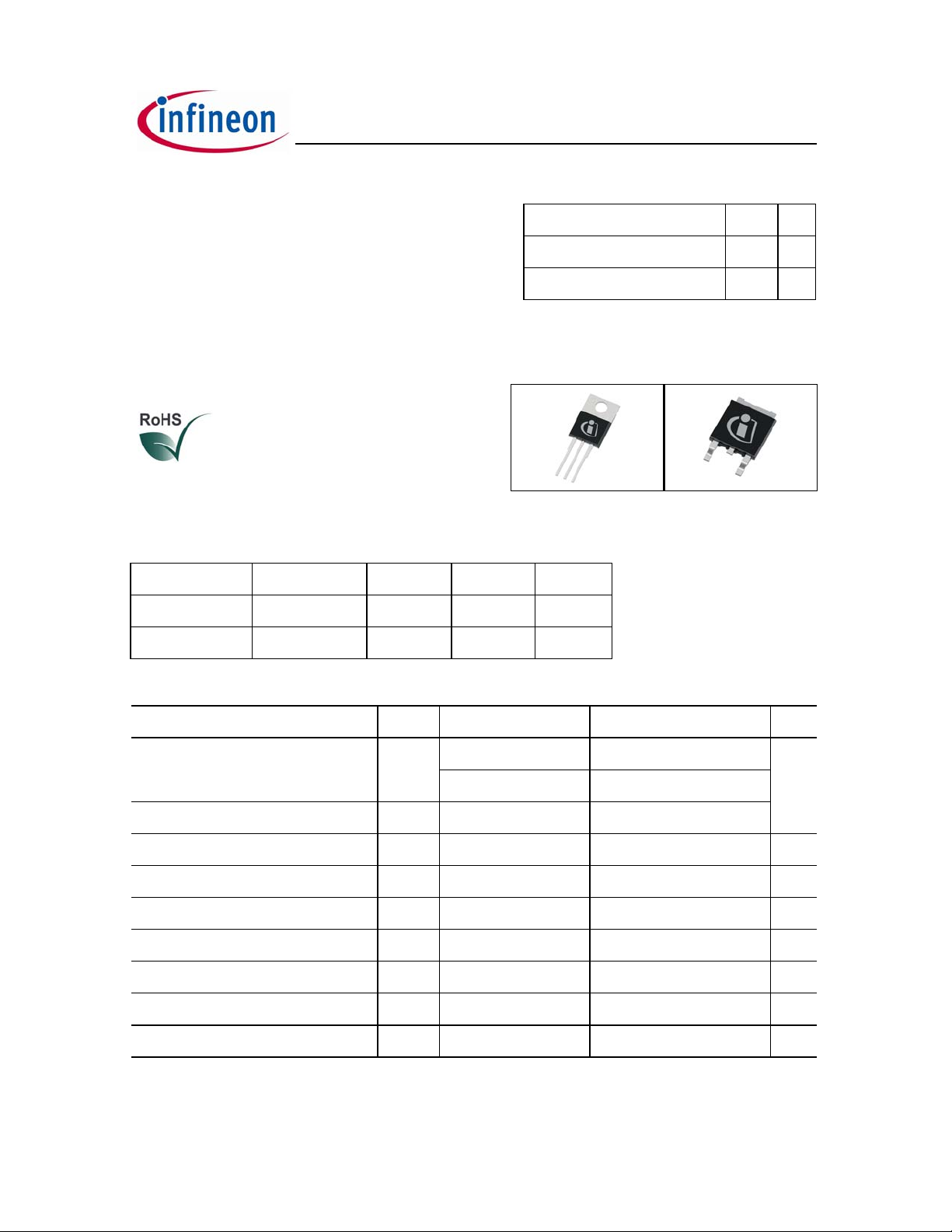
SPP15P10P G
SPD15P10P G
SIPMOS® Small-Signal-Transistor
Product Summary
Features
• P-Channel
• Enhancement mode
• Normal level
• Avalanche rated
• Pb-free lead plating; RoHS compliant
Type Package Marking Lead free Packing
SPP15P10P G PG-TO220-3 15P10P Yes Non dry
V
DS
R
DS(on),max
I
D
PG-TO252-3PG-TO220-3
-100 V
0.24
-15 A
Ω
SPD15P10P G PG-TO252-3 15P10P Yes Non dry
Maximum ratings, at T
Parameter Symbol Conditions Unit
Continuous drain current
Pulsed drain current
Avalanche energy, single pulse
Gate source voltage
Power dissipation
Operating and storage temperature
ESD Class
Soldering temperature
IEC climatic category; DIN IEC 68-1
=25 °C, unless otherwise specified
j
I
D
I
D,pulse
E
AS
V
GS
P
tot
T
j
, T
TC=25 °C
T
TC=25 °C
ID=-15 A, R
TC=25 °C
stg
=100 °C
C
GS
=25 Ω
Value
-15
-10.6
-60
230
±20
128
-55 ... 175
1C (1kV to 2kV)
260 °C
55/175/56
A
mJ
V
W
°C
Rev 1.5 page 1 2008-09-01

SPP15P10P G
SPD15P10P G
Parameter Symbol Conditions Unit
Values
min. typ. max.
Thermal characteristics
Thermal resistance,
junction - soldering point
Thermal resistance,
junction - ambient
Electrical characteristics, at T
R
thJC
R
thJA
minimal footprint,
steady state
2
6 cm
cooling area1),
steady state
=25 °C, unless otherwise specified
j
- - 1.17 K/W
--75
--45
Static characteristics
Drain-source breakdown voltage
Gate threshold voltage
V
(BR)DSSVGS
V
GS(th)
=0 V, ID=-1 mA
VDS=VGS, ID=-
1.54 mA
-100 - - V
-4 -3 -2.1
Zero gate voltage drain current
Gate-source leakage current
Drain-source on-state resistance
Transconductance
1)
Device on 40 mm x 40 mm x 1.5 mm epoxy PCB FR4 with 6 cm2 (one layer, 70 µm thick) copper area for drain
connection. PCB is vertical in still air.
I
I
R
g
DSS
GSS
DS(on)
fs
VDS=-100 V, VGS=0 V,
T
=25 °C
j
V
=-100 V, VGS=0 V,
DS
T
=150 °C
j
VGS=-20 V, VDS=0 V
VGS=-10 V,
I
=-10.6 A
D
|VDS|>2|ID|R
I
=-10.6 A
D
DS(on)max
,
- -0.1 -1 µA
- -10 -100
- -10 -100 nA
- 160 240
4.7 9.3 - S
mΩ
Rev 1.5 page 2 2008-09-01

SPP15P10P G
g
SPD15P10P G
Parameter Symbol Conditions Unit
Values
min. typ. max.
Dynamic characteristics
Input capacitance
Output capacitance
Reverse transfer capacitance
Turn-on delay time
Rise time
Turn-off delay time
Fall time
Gate Char
e Characteristics
Gate to source charge
Gate to drain charge
Gate charge total
2)
C
C
C
t
t
t
t
Q
Q
Q
iss
oss
rss
d(on)
r
d(off)
f
gs
gd
g
V
=0 V, VDS=-25 V,
GS
f =1 MHz
VDD=-50 V,
V
=-10 V,
GS
=-15 A, R
I
D
=-80 V, ID=-15 A,
V
DD
V
=0 to -10 V
GS
G
=6 Ω
- 961 1280 pF
- 237 315
- 100 150
- 9.5 15.9 ns
-2333
-3343
-1620
- 5.4 7.2 nC
-1827
-3748
Gate plateau voltage
V
plateau
Reverse Diode
Diode continuous forward current
Diode pulse current
Diode forward voltage
Reverse recovery time
Reverse recovery charge
2)
See figure 16 for gate charge parameter definition
I
S
I
S,pulse
V
SD
t
rr
Q
rr
TC=25 °C
VGS=0 V, IF=-15 A,
T
=25 °C
j
=50 V, IF=|IS|,
V
R
di
/dt =100 A/µs
F
- 5.9 - V
- - -15 A
--60
- -0.94 -1.35 V
- 100 150 ns
- 419 628 nC
Rev 1.5 page 3 2008-09-01
 Loading...