

PROFET® BTS 740S2
Smart High-Side Power Switch
Two Channels: 2 x 30mΩ
Current Sense
Product Summary Package
Operating Voltage V
bb(on)
5.0...34V
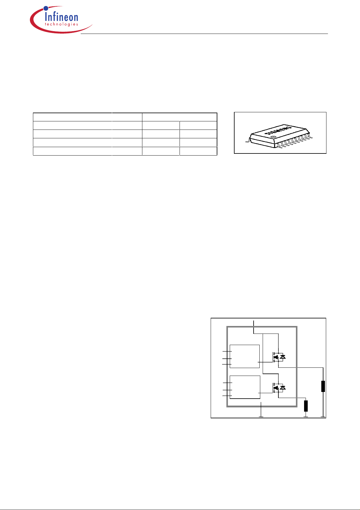
P-DSO-20-9
Active channels one two parallel
On-state Resistance R
Nominal load current I
Current limitation I
ON
L(NOM)
L(SCr)
Ω
30m
5.5A 8.5A
24A 24A
15m
Ω
General Description
•
N channel vertical power MOSFET with charge pump, ground referenced CMOS compatible input,
diagnostic feedback and proportional load current sense monolithically integrated in Smart SIPMOS
technology.
•
Fully protected by embedded protection functions
Applications
•
µC compatible high-side power switch with diagnostic feedback for 12V and 24V grounded loads
•
All types of resistive, inductive and capacitve loads
•
Most suitable for loads with high inrush currents, so as lamps
•
Replaces electromechanical relays, fuses and discrete circuits
Basic Functions
•
CMOS compatible input
•
Undervoltage and overvoltage shutdown with auto-restart and hysteresis
•
Fast demagnetization of inductive loads
•
Logic ground independent from load ground
Protection Functions
•
Short circuit protection
•
Overload protection
•
Current limitation
•
Thermal shutdown
•
Overvoltage protection (including load dump) with external
resistor
•
Reverse battery protection with external resistor
•
Loss of ground and loss of V
•
Electrostatic discharge protection (ESD)
protection
bb
Diagnostic Functions
• Proportinal load current sense
• Diagnostic feedback with open drain output
• Open load detection in OFF-state with external resistor
• Feedback of thermal shutdown in ON-state
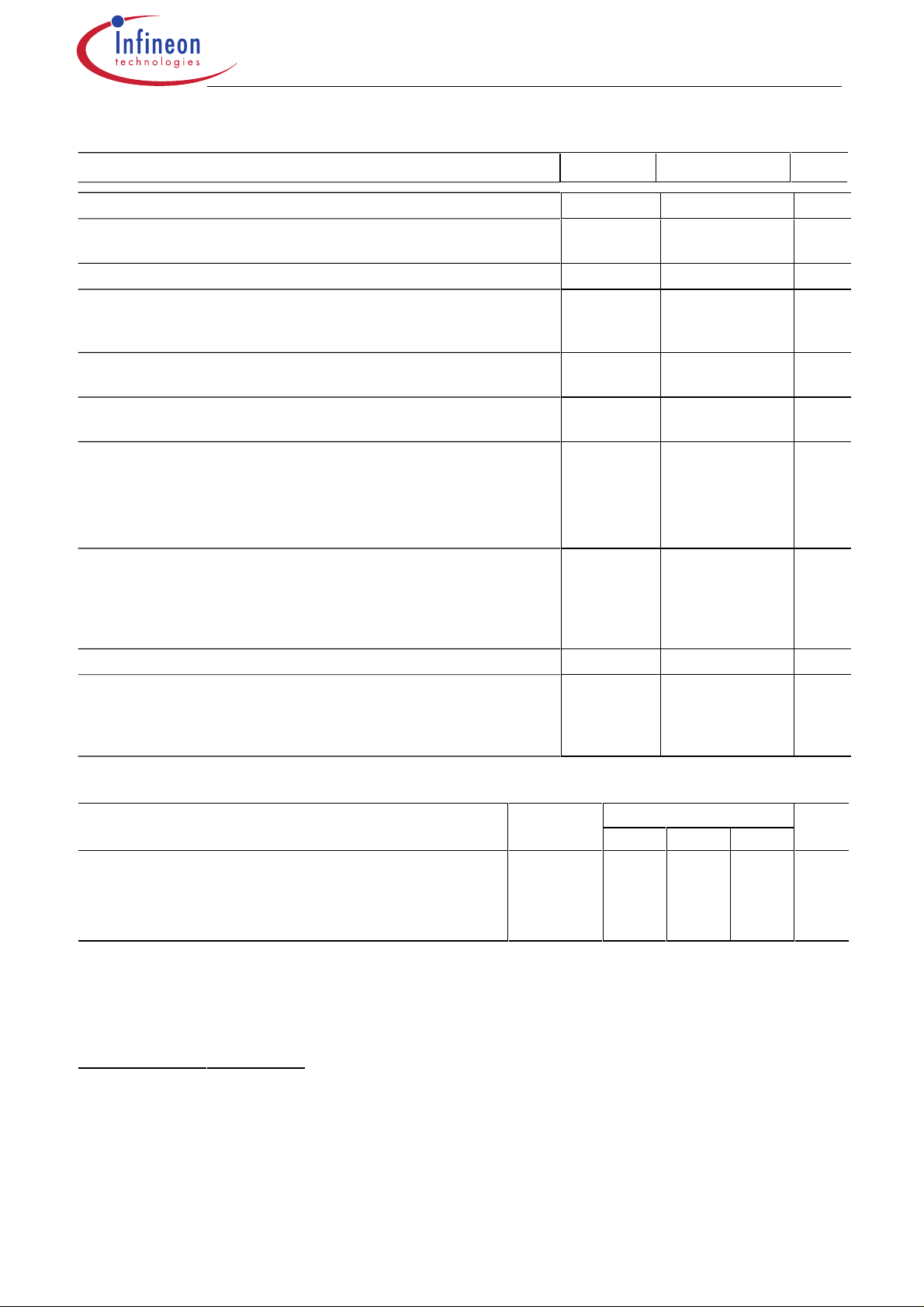
IN1
ST1
IS1
IN2
ST2
IS2
Vbb
Logic
Channel
1
Logic
Channel
2
PROFET
GND
OUT 1
Load 1
OUT 2
Load 2
Data Sheet 1 1999-06-16

Functional diagram
g
y
O
BTS 740S2
IN1
ST1
IS1
GND1
IN2
ST2
IS2
GND2
overvoltage
protection
internal
e suppl
volta
ESD
gate
control
+
charge
logic
pump
temperature
sensor
Open load
detection
Current
sense
Control and protection circuit
of
channel 2
current limit
clamp for
inductive load
R
1
GND1
Channel 1
PROFET
VBB
OUT1
LOAD
OUT2
Pin Definitions and Functions
Pin Symbol Function
1,10,
11,12,
15,16,
19,20
3IN1
7 IN2 logic high signal
17,18 OUT1
13,14 OUT2 of channel 1,2. Both pins of each output have
4 ST1
8 ST2 open drain, invers to input level
2 GND1
6 GND2
5IS1
9IS2
V
bb
Positive power supply voltage. Design the
wiring for the simultaneous max. short circuit
currents from channel 1 to 2 and also for low
thermal resistance
Input 1,2, activates channel 1,2 in case of
Output 1,2, protected high-side power output
to be connected in parallel for operation
according ths spec (e.g. k
). Design the wiring
ilis
for the max. short circuit current
Diagnostic feedback 1,2 of channel 1,2,
Ground 1 of chip 1 (channel 1)
Ground 2 of chip 2 (channel 2)
Sense current output 1,2; proportional to the
load current, zero in the case of current
limitation of the load current
Pin configuration
(top view)
V
1 • 20 V
bb
GND1 2 19 V
IN1 3 18 OUT1
ST1 4 17 OUT1
IS1 5 16 V
GND2 6 15 V
IN2 7 14 OUT2
ST2 8 13 OUT2
IS2 9 12 V
Vbb10 11 V
bb
bb
bb
bb
bb
bb
Data Sheet 2 1999-06-16
BTS 740S2
)
T
T
I
E
I
E
)
(
)
Maximum Ratings at
T
= 25˚C unless otherwise specified
j
Parameter Symbol Values Unit
Supply voltage (overvoltage protection see page 4)
Supply voltage for full short circuit protection
T
= -40 ...+150˚C
j,start
Load current (Short-circuit current, see page 5)
Load dump protection1)
2)
R
= 2 Ω,
I
t
= 200 ms; IN = low or high,
d
each channel loaded with
V
LoadDump
R
=
= 7.0 Ω,
L
V
+
V
,
V
s
= 13.5 V
A
A
Operating temperature range
Storage temperature range
Power dissipation (DC
(all channels active)
4)
= 25˚C :
a
= 85˚C :
a
V
bb
V
bb
I
L
V
Load dump
T
j
T
stg
P
tot
43 V
34 V
self-limited A
3
)
-40 ...+150
60 V
˚C
-55 ...+150
3.8
W
2.0
Maximal switchable inductance, single pulse
V
= 12V,
bb
= 5.5 A,
= 8.5 A,
see diagrams on page 10
Electrostatic discharge capability (ESD
Human Body Model
acc. MIL-STD883D, method 3015.7 and ESD assn. std. S5.1-1993
R=1.5kΩ; C=100pF
Input voltage (DC)
Current through input pin (DC)
Current through status pin (DC)
Current through current sense pin (DC)
see internal circuit diagram page 9
T
= 150˚C4),
j,start
= 370 mJ, 0 Ω one channel:
AS
= 790 mJ, 0 Ω two parallel channels:
AS
out to all other pins shorted:
IN:
ST, IS:
Z
V
V
I
I
I
IN
ST
IS
L
ESD
IN
1816mH
1.0
kV
4.0
8.0
-10 ... +16 V
±2.0
mA
±5.0
±14
Thermal Characteristics
Parameter and Conditions Symbol Values Unit
min typ Max
Thermal resistance
junction - soldering point
junction - ambient
4)
4),5)
each channel:
one channel active:
R
R
thjs
thja
all channels active:
1)
Supply voltages higher than V
resistor for the GND connection is recommended.
2)
R
= internal resistance of the load dump test pulse generator
I
3)
V
Load dump
4)
Device on 50mm*50mm*1.5mm epoxy PCB FR4 with 6cm
connection. PCB is vertical without blown air. See page 15
5)
Soldering point: upper side of solder edge of device pin 15. See page 15
is setup without the DUT connected to the generator per ISO 7637-1 and DIN 40839
require an external current limit for the GND and status pins (a 150Ω
bb(AZ)
2
(one layer, 70µm thick) copper area for V
-- -- 12
--
--
40
33
K/W
--
--
bb
Data Sheet 3 1999-06-16
BTS 740S2
T
j
g
T
j
Electrical Characteristics
Parameter and Conditions, each of the two channels Symbol Values Unit
at Tj = -40...+150˚C,
Load Switching Capabilities and Characteristics
V
= 12 V unless otherwise specified
bb
min typ max
On-state resistance (Vbb to OUT);
each channel,
two parallel channels,
IL = 5 A
T
T
= 25˚C :
j
= 150˚C:
j
T
= 25˚C:
j
Output voltage drop limitation at small load
currents,
I
= 0.5 A
L
see page 14
T
=-40...+150˚C:
j
Nominal load current one channel active:
two parallel channels active:
Device on PCB
6)
T
,
a
= 85˚C,
T
≤ 150˚C
j
Output current while GND disconnected or pulled up;
V
= 30 V,
bb
see diagram page 9; (not tested specified by design)
Turn-on time7) IN to 90%
Turn-off time IN
R
= 12 Ω
L
Slew rate on
10 to 30%
Slew rate off
70 to 40%
V
= 0,
IN
V
OUT
V
V
7)
OUT
7)
OUT
,
R
,
R
= 12 Ω:
L
= 12 Ω:
L
to 10%
V
OUT
:
:
R
V
I
I
t
t
d
-dV/dt
ON
ON(NL)
L(NOM)
L(GNDhigh)
on
off
V
/dt
on
off
--
27
54
14
30
60
15
mΩ
-- 50 -- mV
4.9
7.8
5.5
8.5
-- A
-- -- 8 mA
25
25
70
80
150
200
µs
0.1 -- 1 V/µs
0.1 -- 1 V/µs
Operating Parameters
Operating voltage
Undervoltage shutdown
Undervoltage restart
8)
=-40...+25˚C:
T
=+150˚C:
j
V
bb(on)
V
bb(under)
V
bb(u rst)
5.0 -- 34 V
3.2 -- 5.0 V
-- 4.5 5.5
6.0
Undervoltage restart of charge pump
see dia
Undervoltage hysteresis
∆
V
bb(under)
Overvoltage shutdown
Overvoltage restart
Overvoltage hysteresis ∆
6)
Device on 50mm*50mm*1.5mm epoxy PCB FR4 with 6cm
connection. PCB is vertical without blown air. See page 15
)
7
See timing diagram on page 11.
8)
At supply voltage increase up to
ram page 13
V
=
bb(u rst)
-
V
bb(under)
=-40...+25˚C:
T
=150˚C:
j
V
∆
V
V
2
(one layer, 70µm thick) copper area for V
V
= 4.7 V typ without charge pump,
bb
bb(ucp)
V
bb(under)
bb(over)
bb(o rst)
V
bb(over)
V
--
--
4.7
--
-- 0.5 -- V
34 -- 43 V
33 -- -- V
-- 1 -- V
≈
V
OUT
bb
- 2 V
6.5
7.0
bb
Data Sheet 4 1999-06-16
V
V
BTS 740S2
T
j
Parameter and Conditions, each of the two channels Symbol Values Unit
at Tj = -40...+150˚C,
V
= 12 V unless otherwise specified
bb
min typ max
Overvoltage protection
I
=40 mA
bb
Standby current
V
IN
see diagram page 10
= 0;
10
Leakage output current (included in
V
IN = 0
Operating current
I
=
I
+
GND
GND1
I
GND2
9)
T
=+25...+150˚C:
)
11)
,
V
= 5V,
IN
j
T
=-40˚C...25˚C:
j
I
bb(off)
, one channel on:
two channels on:
Protection Functions
Current limit,
(see timing diagrams, page 12)
Repetitive short circuit current limit,
T
=
T
each channel
j
jt
two parallel channels
(see timing diagrams, page 12)
Initial short circuit shutdown time
(see timing diagrams on page 12)
T
Output clamp (inductive load switch off)
at V
ON(CL)
= Vbb - V
OUT
,
I
L
= 40 mA
=25˚C...150˚C:
T
j
Thermal overload trip temperature
Thermal hysteresis
=-40:
T
=150˚C:
j
)
=-40˚C:
T
j
=25˚C:
T
j
=+150˚C:
T
j
=25˚C:
j,start
12)
=-40˚C:
T
j
V
bb(AZ)
I
bb(off)
I
L(off)
I
GND
I
L(lim)
I
L(SCr)
t
off(SC)
V
ON(CL)
T
jt
∆
T
jt
41
43
--
--
47
24
--
--
52
8
30
µA
50
-- -- 20 µA
--
--
48
40
31
--
--
1.2
2.4
56
50
37
24
24
36mA
65
58
45
--
--
-- 2.0 -- ms
41
43
47
--
--
52
150 -- -- ˚C
-- 10 -- K
V
A
A
V
Reverse Battery
Reverse battery voltage
Drain-source diode voltage (V
= - 4.0 A,
I
L
9)
Supply voltages higher than V
resistor in the GND connection is recommended). See also
circuit diagram page 9.
10)
Measured with load; for the whole device; all channels off
11)
Add
)
12
If channels are connected in parallel, output clamp is usually accomplished by the channel with the lowest
V
ON(CL)
13)
Requires a 150 Ω resistor in GND connection. The reverse load current through the intrinsic drain-source
diode has to be limited by the connected load. Power dissipation is higher compared to normal operating
conditions due to the voltage drop across the drain-source diode. The temperature protection is not active
during reverse current operation! Input and Status currents have to be limited (see max. ratings page 3 and
circuit page 9).
T
j = +150˚C
I
, if
I
ST
> 0
ST
13)
-
V
bb
out
bb(AZ)
bb
require an external current limit for the GND and status pins (a 150 Ω
)
> V
V
-
V
ON(CL)
ON
in table of protection functions and
-- -- 32 V
-- 600 -- mV
Data Sheet 5 1999-06-16
 Loading...