

INFINEON BTS721L1 User Manual
PROFET
Smart Four Channel Highside Power Switch
Features
•
Overload protection
•
Current limitation
•
Short-circuit protection
•
Thermal shutdown
•
Overvoltage protection
(including load dump)
•
Fast demagnetization of inductive loads
1
•
Reverse battery protection
•
Undervoltage and overvoltage shutdown
with auto-restart and hysteresis
•
Open drain diagnostic output
)
• Open load detection in ON-state
•
CMOS compatible input
•
Loss of ground and loss of V
•
Electrostatic discharge (ESD) protection
protection
bb
Application
•
µC compatible power switch with diagnostic feedback
for 12 V and 24 V DC grounded loads
•
All types of resistive, inductive and capacitive loads
•
Replaces electromechanical relays and discrete circuits
Product Summary
Overvoltage Protection V
Operating voltage
V
active channels: one
On-state resistance R
Nominal load current I
Current limitation I
100 50 25
ON
L(NOM)
L(SCr)
2.9 4.3 6.3 A
8 8 8 A
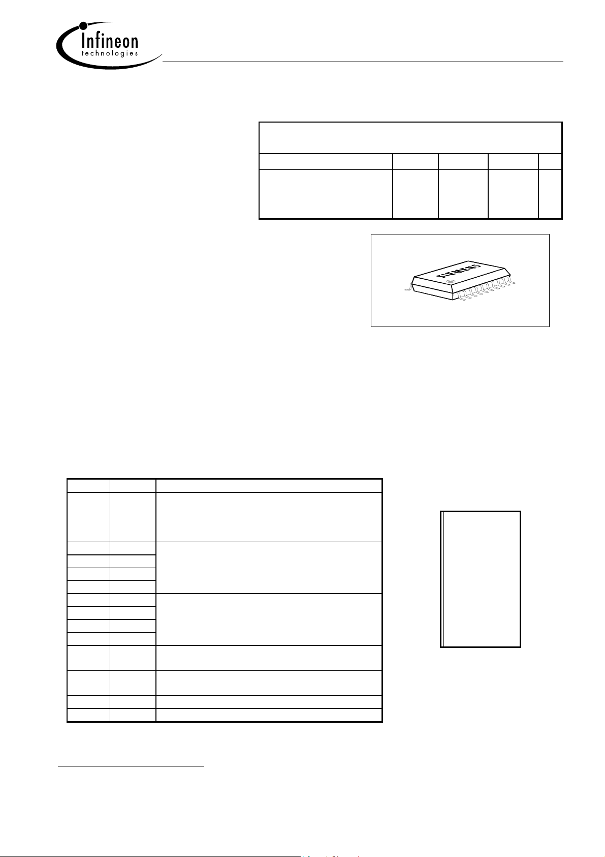
P-DSO-20
43 V
bb(AZ)
5.0 ... 34 V
bb(on)
two parallel four parallel
®
BTS721L1
mΩ
General Description
N channel vertical power FET with charge pump, ground referenced CMOS compatible input and diagnostic
feedback, monolithically integrated in Smart SIPMOS technology. Providing embedded protective functions.
Pin Definitions and Functions
Pin Symbol Function
1,10,
11,12,
15,16,
19,20
V
Positive power supply voltage. Design the
bb
wiring for the simultaneous max. short circuit
currents from channel 1 to 4 and also for low
thermal resistance
3 IN1 Input 1 .. 4, activates channel 1 .. 4 in case of
5 IN2 logic high signal
7 IN3
9 IN4
18 OUT1 Output 1 .. 4, protected high-side power output
17 OUT2 of channel 1 .. 4. Design the wiring for the
14 OUT3 max. short circuit current
13 OUT4
4 ST1/2 Diagnostic feedback 1/2 of channel 1 and
channel 2, open drain, low on failure
8 ST3/4 Diagnostic feedback 3/4 of channel 3 and
channel 4, open drain, low on failure
2 GND1/2 Ground 1/2 of chip 1 (channel 1 and channel 2)
6 GND3/4 Ground 3/4 of chip 2 (channel 3 and channel 4)
Pin configuration (top view)
V
1 • 20 V
bb
GND1/2 2 19 Vbb
IN1 3 18 OUT1
ST1/2 4 17 OUT2
IN2 5 16 Vbb
GND3/4 6 15 Vbb
IN3 7 14 OUT3
ST3/4 8 13 OUT4
IN4 9 12 Vbb
Vbb 10 11 Vbb
bb
1)
With external current limit (e.g. resistor R
=150 Ω) in GND connection, resistor in series with ST
GND
connection, reverse load current limited by connected load.
Semiconductor Group 1 of 15 2003-Oct-01
BTS721L1
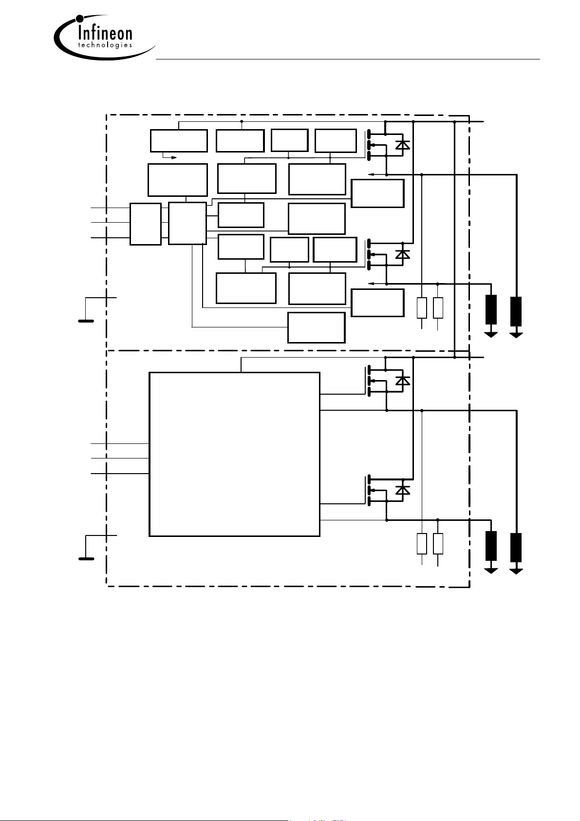
Block diagram
Four Channels; Open Load detection in on state;
+ V
Voltage
source
V
Logic
Voltage
sensor
3
IN1
IN2
5
4
ST1/2
ESD
Logic
Overvoltage
protection
Level shifter
Rectifier 1
Charge
pump 1
Charge
pump 2
Current
limit 1
Current
limit 2
Gate 1
protection
Limit for
unclamped
ind. loads 1
Open load
Short to Vbb
detection 1
Gate 2
protection
Temperature
sensor 1
bb
Channel 1
OUT1
Channel 2
Leadframe
18
Signal GND
Chip 1
Signal GND
Chip 2
2
8
6
7
9
GND1/2
IN3
IN4
ST3/4
GND3/4
Chip 1
PROFET
Chip 2
Level shifter
Rectifier 2
Short to Vbb
Logic and protection circuit of chip 2
(equivalent to chip 1)
Limit for
unclamped
ind. loads 2
Open load
detection 2
Temperature
sensor 2
OUT2
RR
O1
RR
O3
GND1/2
+ V
Channel 3
OUT3
Channel 4
OUT4
GND3/4
O2
bb
O4
17
Load
Load GND
Leadframe
14
13
Load
Load GND
Leadframe connected to pin 1, 10, 11, 12, 15, 16, 19, 20
Semiconductor Group 2 2003-Oct-01

BTS721L1
Maximum Ratings at Tj = 25°C unless otherwise specified
Parameter Symbol Values Unit
Supply voltage (overvoltage protection see page 4) Vbb 43 V
Supply voltage for full short circuit protection
T
= -40 ...+150°C
j,start
Vbb 34 V
Load current (Short-circuit current, see page 5) IL self-limited A
Load dump protection2) V
3)
R
= 2 Ω, td = 200 ms; IN = low or high,
I
LoadDump
each channel loaded with R
Operating temperature range
Storage temperature range
Power dissipation (DC)5 Ta = 25°C:
= UA + Vs, UA = 13.5 V
= 4.7 Ω,
L
V
Load
4
)
dump
Tj
T
stg
P
3.7
tot
(all channels active) Ta = 85°C:
Inductive load switch-off energy dissipation, single pulse
V
= 12V, T
bb
j,start
= 150°C5),
IL = 2.9 A, ZL = 58 mH, 0 Ω one channel:
EAS
IL = 4.3 A, ZL = 58 mH, 0 Ω two parallel channels:
IL = 6.3 A, ZL = 58 mH, 0 Ω four parallel channels:
see diagrams on page 9 and page 10
Electrostatic discharge capability (ESD)
V
1.0 kV
ESD
(Human Body Model)
Input voltage (DC) VIN -10 ... +16 V
Current through input pin (DC)
Current through status pin (DC)
IIN
IST
see internal circuit diagram page 8
Thermal resistance
junction - soldering point
5),6)
each channel:
junction - ambient5) one channel active:
all channels active:
R
thjs
R
thja
60 V
-40 ...+150
°C
-55 ...+150
W
1.9
0.3
J
0.65
1.5
±2.0
mA
±5.0
15 K/W
41
34
2)
Supply voltages higher than V
150 Ω resistor in the GND connection and a 15 kΩ resistor in series with the status pin. A resistor for input
protection is integrated.
3)
RI = internal resistance of the load dump test pulse generator
4)
V
Load dump
5)
Device on 50mm*50mm*1.5mm epoxy PCB FR4 with 6cm
connection. PCB is vertical without blown air. See page 15
6)
Soldering point: upper side of solder edge of device pin 15. See page 15
is setup without the DUT connected to the generator per ISO 7637-1 and DIN 40839
require an external current limit for the GND and status pins, e.g. with a
bb(AZ)
2
(one layer, 70µm thick) copper area for Vbb
Semiconductor Group 3 2003-Oct-01

BTS721L1
Electrical Characteristics
Parameter and Conditions, each of the four channels Symbol Values Unit
at Tj = 25 °C, Vbb = 12 V unless otherwise specified
Load Switching Capabilities and Characteristics
min typ max
On-state resistance (Vbb to OUT)
IL = 2 A each channel, Tj = 25°C:
T
= 150°C:
j
two parallel channels, Tj = 25°C:
four parallel channels, Tj = 25°C:
Nominal load current one channel active:
two parallel channels active:
four parallel channels active:
Device on PCB5), Ta = 85°C, Tj ≤ 150°C
Output current while GND disconnected or pulled
up; V
Turn-on time to 90% V
Turn-off time to 10% V
= 30 V, V
bb
= 0, see diagram page 9
IN
OUT
OUT
RL = 12 Ω, Tj =-40...+150°C
Slew rate on
10 to 30% V
OUT
, R
= 12 Ω, Tj =-40...+150°C:
L
Slew rate off
70 to 40% V
, RL = 12 Ω, Tj =-40...+150°C:
OUT
RON
I
I
:
ton
:
t
2.5
L(NOM)
L(GNDhigh)
off
-- -- 10 mA
--
3.8
5.9
80
80
85
170
43
22
2.9
100
200
50
25
-- A
4.3
6.3
200
200
400
400
dV/dton 0.1 -- 1 V/µs
-dV/dt
0.1 -- 1 V/µs
off
mΩ
µs
Operating Parameters
Operating voltage7) Tj =-40...+150°C: V
Undervoltage shutdown Tj =-40...+150°C: V
Undervoltage restart Tj =-40...+25°C:
V
5.0 -- 34 V
bb(on)
bb(under)
bb(u rst)
3.5 -- 5.0 V
-- -- 5.0
Tj =+150°C:
Undervoltage restart of charge pump
V
bb(ucp)
-- 5.6 7.0 V
see diagram page 14 Tj =-40...+150°C:
Undervoltage hysteresis
∆V
bb(under)
= V
bb(u rst)
- V
bb(under)
Overvoltage shutdown Tj =-40...+150°C: V
Overvoltage restart Tj =-40...+150°C: V
Overvoltage hysteresis Tj =-40...+150°C: ∆V
Overvoltage protection
I
= 40 mA
bb
8)
Tj =-40...+150°C:
Standby current, all channels off Tj =25°C:
V
= 0 T
IN
7)
At supply voltage increase up to V
8)
see also V
in circuit diagram on page 8.
ON(CL)
= 5.6 V typ without charge pump, V
bb
=150°C:
j
∆V
bb(under)
34 -- 43 V
bb(over)
33 -- -- V
bb(o rst)
-- 0.5 -- V
42 47 -- V
--
V
bb(AZ)
I
bb(off)
bb(over)
V
7.0
-- 0.2 -- V
≈Vbb - 2 V
OUT
--
28
44
60
70
µA
Semiconductor Group 4 2003-Oct-01
BTS721L1
Parameter and Conditions, each of the four channels Symbol Values Unit
at Tj = 25 °C, Vbb = 12 V unless otherwise specified
Leakage output current (included in I
= I
GND1/2
+ I
= 5V, Tj =-40...+150°C
IN
, one channel on:
GND3/4
VIN = 0
Operating current 9), V
I
GND
four channels on:
bb(off)
)
I
-- -- 12 µA
L(off)
I
GND
min typ max
--
--
2
8
312mA
Protection Functions
Initial peak short circuit current limit, (see timing
diagrams, page 12)
each channel,
10)
=-40°C:
j
T
=25°C:
Tj
=+150°C:
Tj
I
L(SCp)
11
9
5
18
14
8
25
22
14
A
two parallel channels twice the current of one channel
four parallel channels four times the current of one channel
Repetitive short circuit current limit,
Tj = Tjt each channel
two parallel channels
four parallel channels
(see timing diagrams, page 12)
Initial short circuit shutdown time T
T
(see page 12 and timing diagrams on page 12)
Output clamp (inductive load switch off)
at V
ON(CL)
= Vbb - V
OUT
j,start
j,start
11)
=-40°C:
= 25°C:
I
--
L(SCr)
t
V
--
off(SC)
-- 47 -- V
ON(CL)
--
--
--
8
8
8
3.8
3
--
--
--
----ms
A
Thermal overload trip temperature Tjt 150 -- -- °C
Thermal hysteresis
∆
Tjt -- 10 -- K
Reverse Battery
Reverse battery voltage
Drain-source diode voltage (V
= - 2.9 A, Tj = +150°C
IL
9)
Add I
10)
Integrated protection functions are designed to prevent IC destruction under fault conditions described in the
data sheet. Fault conditions are considered as "outside" normal operating range. Protection functions are not
designed for continuous repetitive operation.
11)
If channels are connected in parallel, output clamp is usually accomplished by the channel with the lowest
V
12)
Requires a 150 Ω resistor in GND connection. The reverse load current through the intrinsic drain-source
diode has to be limited by the connected load. Note that the power dissipation is higher compared to normal
operating conditions due to the voltage drop across the intrinsic drain-source diode. The temperature
protection is not active during reverse current operation! Input and Status currents have to be limited (see
max. ratings page 3 and circuit page 8).
ST
ON(CL)
, if IST > 0
12)
-Vbb -- -- 32 V
out
> V
bb
)
-VON -- 610 -- mV
Semiconductor Group 5 2003-Oct-01
 Loading...