


Target Data Sheet, V1.2, August 2006
BTS 5242-2L
Smart High-Side Power Switch
PROFET
Two Channels, 25 mΩ
Automotive Power
Never stop thinking.

Smart High-Side Power Switch
BTS 5242-2L
Table of Contents Page
Product Summary . . . . . . . . . . . . . . . . . . . . . . . . . . . . . . . . . . . . . . . . . . . . . . . . . . . . . . . . . . . 3
1 Overview . . . . . . . . . . . . . . . . . . . . . . . . . . . . . . . . . . . . . . . . . . . . . . . . . . . . . . . . . . . . . . . . 5
1.1 Block Diagram . . . . . . . . . . . . . . . . . . . . . . . . . . . . . . . . . . . . . . . . . . . . . . . . . . . . . . . . . 5
1.2 Terms . . . . . . . . . . . . . . . . . . . . . . . . . . . . . . . . . . . . . . . . . . . . . . . . . . . . . . . . . . . . . . . . 6
2 Pin Configuration . . . . . . . . . . . . . . . . . . . . . . . . . . . . . . . . . . . . . . . . . . . . . . . . . . . . . . . . . 7
2.1 Pin Assignment BTS 5242-2L . . . . . . . . . . . . . . . . . . . . . . . . . . . . . . . . . . . . . . . . . . . . . 7
2.2 Pin Definitions and Functions . . . . . . . . . . . . . . . . . . . . . . . . . . . . . . . . . . . . . . . . . . . . . 7
3 Electrical Characteristics . . . . . . . . . . . . . . . . . . . . . . . . . . . . . . . . . . . . . . . . . . . . . . . . . . . 8
3.1 Maximum Ratings . . . . . . . . . . . . . . . . . . . . . . . . . . . . . . . . . . . . . . . . . . . . . . . . . . . . . . 8
4 Block Description and Electrical Characteristics . . . . . . . . . . . . . . . . . . . . . . . . . . . . . . 10
4.1 Power Stages . . . . . . . . . . . . . . . . . . . . . . . . . . . . . . . . . . . . . . . . . . . . . . . . . . . . . . . . . 10
4.1.1 Output On-State Resistance . . . . . . . . . . . . . . . . . . . . . . . . . . . . . . . . . . . . . . . . . 10
4.1.2 Input Circuit . . . . . . . . . . . . . . . . . . . . . . . . . . . . . . . . . . . . . . . . . . . . . . . . . . . . . 10
4.1.3 Inductive Output Clamp . . . . . . . . . . . . . . . . . . . . . . . . . . . . . . . . . . . . . . . . . . . . 11
4.1.4 Electrical Characteristics . . . . . . . . . . . . . . . . . . . . . . . . . . . . . . . . . . . . . . . . . . . 13
4.2 Protection Functions . . . . . . . . . . . . . . . . . . . . . . . . . . . . . . . . . . . . . . . . . . . . . . . . . . . . 15
4.2.1 Over Load Protection . . . . . . . . . . . . . . . . . . . . . . . . . . . . . . . . . . . . . . . . . . . . . . 15
4.2.2 Reverse Polarity Protection . . . . . . . . . . . . . . . . . . . . . . . . . . . . . . . . . . . . . . . . . . 16
4.2.3 Over Voltage Protection . . . . . . . . . . . . . . . . . . . . . . . . . . . . . . . . . . . . . . . . . . . . 16
4.2.4 Loss of Ground Protection . . . . . . . . . . . . . . . . . . . . . . . . . . . . . . . . . . . . . . . . . . 17
4.2.5 Electrical Characteristics . . . . . . . . . . . . . . . . . . . . . . . . . . . . . . . . . . . . . . . . . . . 18
4.3 Diagnosis . . . . . . . . . . . . . . . . . . . . . . . . . . . . . . . . . . . . . . . . . . . . . . . . . . . . . . . . . . . . 20
4.3.1 ON-State Diagnosis . . . . . . . . . . . . . . . . . . . . . . . . . . . . . . . . . . . . . . . . . . . . . . . . 21
4.3.2 OFF-State Diagnosis . . . . . . . . . . . . . . . . . . . . . . . . . . . . . . . . . . . . . . . . . . . . . . . 23
4.3.3 Electrical Characteristics . . . . . . . . . . . . . . . . . . . . . . . . . . . . . . . . . . . . . . . . . . . 24
5 Package Outlines BTS 5242-2L . . . . . . . . . . . . . . . . . . . . . . . . . . . . . . . . . . . . . . . . . . . . . 26
6 Revision History . . . . . . . . . . . . . . . . . . . . . . . . . . . . . . . . . . . . . . . . . . . . . . . . . . . . . . . . . 27
Target Data Sheet 2 V1.2, 2006-08-14
Smart High-Side Power Switch
PROFET
Product Summary
The BTS 5242-2L is a dual channel high-side power switch
in PG-DSO-12-9 package providing embedded protective
functions.
The power transistor is built by a N-channel vertical power
MOSFET with charge pump. The device is monolithically
integrated in Smart
Operating voltage V
Over voltage protection V
SIPMOS technology.
bb(on)
bb(AZ)
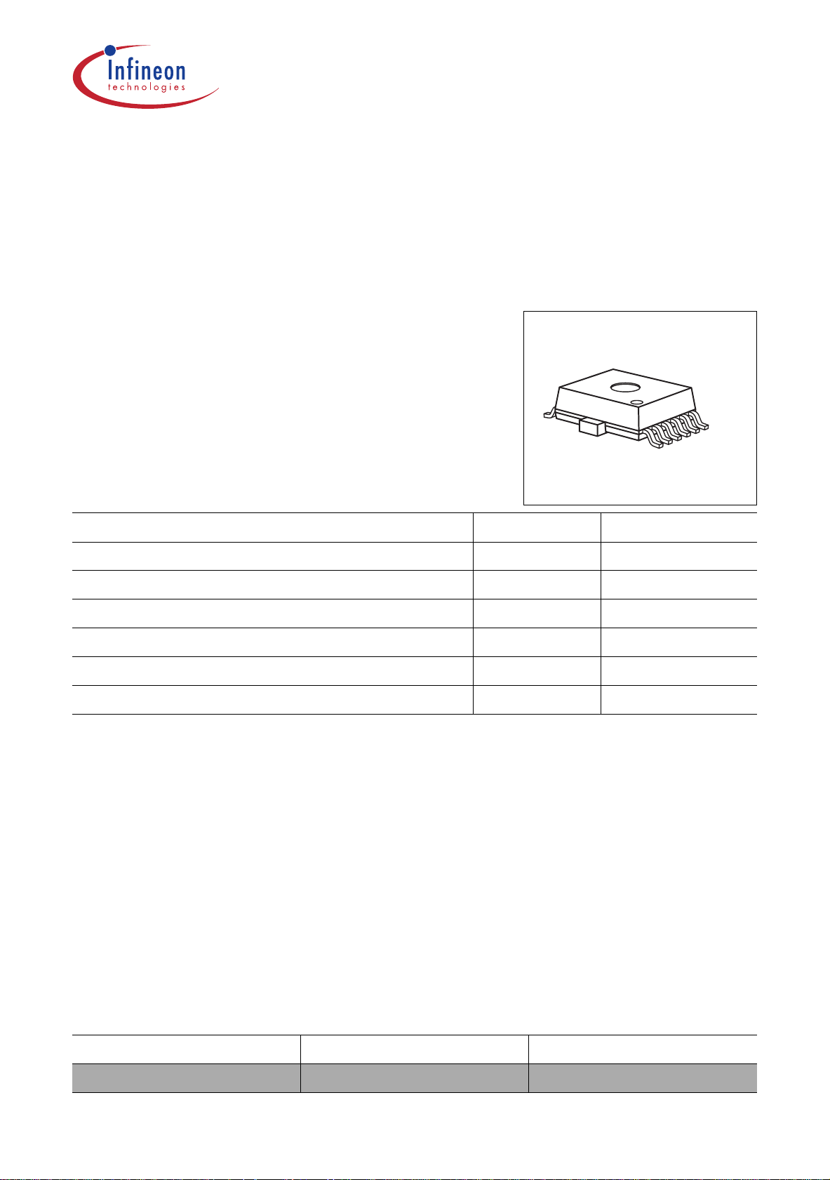
BTS 5242-2L
PG-DSO-12-9
4.5 .. 28 V
41 V
On-State resistance R
Nominal load current (one channel active) I
Adjustable current limitation I
Current limitation repetitive I
Standby current for whole device with load I
Basic Features
• Very low standby current
•3.3 V and 5 V compatible logic pins
• Improved electromagnetic compatibility (EMC)
• Stable behavior at under voltage
• Logic ground independent from load ground
• Secure load turn-off while logic ground disconnected
• Very low leakage current from OUT to GND
• Green product (RoHS compliant)
DS(ON)
L(nom)
L(LIM)
L(SCr)
bb(OFF)
25 mΩ
6 A
7 A / 40 A
7 A / 40 A
7.5 µA
Type Ordering Code Package
BTS 5242-2L On request PG-DSO-12-9
Target Data Sheet 3 V1.2, 2006-08-14

Smart High-Side Power Switch
Protective Functions
• Reverse battery protection with external resistor
• Short circuit protection
• Overload protection
• Multi-step current limitation
• Adjustable current limitation
• Thermal shutdown with restart
• Over voltage protection with external resistor
• Loss of ground and loss of Vbb protection
• Electrostatic discharge protection (ESD)
Diagnostic Functions
• IntelliSense functionality for each channel
• Proportional load current sense signal by current source
• Open load detection in ON-state by load current sense
• Open load detection in OFF-state by voltage source
• Feedback on over temperature and current limitation in ON-state
• Suppressed thermal toggling of fault signal
BTS 5242-2L
Applications
• µC compatible high-side power switch with diagnostic feedback for 12 V grounded loads
• All types of resistive, inductive and capacitive loads
• Most suitable for loads with high inrush currents, so as lamps
• Replaces electromechanical relays, fuses and discrete circuits
Target Data Sheet 4 V1.2, 2006-08-14
Smart High-Side Power Switch
BTS 5242-2L
Overview
1Overview
The BTS 5242-2L is a dual channel high-side power switch (two times 25 mΩ) in PG-DSO-12-9
power package providing embedded protective functions. Integrated resistors at each input pin
(IN1, IN2, CLA) reduce external components.
The load current limitation can be adjusted in two steps by the current limit adjust pin (CLA).
The IntelliSense pins IS1 and IS2 provide a sophisticated diagnostic feedback signal including
current sense function, open load in off state and over load alert.
The power transistor is built by a N-channel vertical power MOSFET with charge pump. The
inputs are ground referenced CMOS compatible. The device is monolithically integrated in
Smart
1.1 Block Diagram
SIPMOS technology.
channel 1
VBB
IN1
IS1
CLA
IN2
IS2
internal
power
supply
ESD
protecti on
channel 2
load cur r ent
sense
gate control
&
logic
control and protection circuit
char ge pum p
open load
detec tion
tem peratur e
sensor
equival ent to
channel 1
GND
cl am p for
inductive load
multi step
load current
limitation
OUT1
OUT2
Figure 1 Block Diagram
Target Data Sheet 5 V1.2, 2006-08-14
Smart High-Side Power Switch
BTS 5242-2L
1.2 Terms
Following figure shows all terms used in this target data sheet.
V
bb
V
IN1
V
IN2
V
Figure 2 Terms
IS1
I
IN1
IN1
I
IN2
IN2
I
IS1
IS1
I
IS2
BTS 5242-2L
IS2
V
IS2
I
CL A
CLA
V
CL A
VBB
GND
I
bb
I
GND
OUT1
OUT2
Overview
I
L1
I
L2
V
V
V
V
OUT1
DS2
OUT2
DS1
Ter m s2 ch . em f
Target Data Sheet 6 V1.2, 2006-08-14
Smart High-Side Power Switch
BTS 5242-2L
2 Pin Configuration
2.1 Pin Assignment BTS 5242-2L
(top view)
GND
IN1
IS1
IS2
IN2
VBB
1
2
3
4
5
6
12
11
10
9
8
7
heat slug (VBB)
Pin Configuration
VBB
OUT1
OUT1
OUT2
OUT2
CLA
Figure 3 Pin Configuration PG-DSO-12-9
2.2 Pin Definitions and Functions
Pin Symbol I/O
OD
2 IN1 I Input signal for channel 1
5 IN2 I Input signal for channel 2
3 IS1 O Diagnosis output signal channel 1
4 IS2 O Diagnosis output signal channel 2
7 CLA I Current limit adjust input for channel 1&2
10,11 OUT1
8, 9 OUT2
1)
1)
O Protected high-side power output channel 1
O Protected high-side power output channel 2
1 GND - Ground connection
6,12,
VBB - Positive power supply for logic supply as well as output
heat slug
Function
power supply
1)
All output pins of each channel have to be connected
Target Data Sheet 7 V1.2, 2006-08-14
Smart High-Side Power Switch
BTS 5242-2L
Electrical Characteristics
3 Electrical Characteristics
3.1 Maximum Ratings
Stresses above the ones listed here may cause permanent damage to the device. Exposure to
maximum rating conditions for extended periods may affect device reliability.
T
= 25 °C (unless otherwise specified)
j
Pos. Parameter Symbol Limit Values Unit Test
Conditions
t ≤ 100 h
R = 0.2 Ω
1)
Power Supply
3.1.1 Supply voltage V
3.1.2 Current through ground pin I
3.1.3 Supply voltage for full short
V
circuit protection (single pulse)
(Tj = -40°C .. 150°C)
bb
GND
bb(SC)
min. max.
18
V
28
-150 mA t ≤ 2 min
0 28 V L = 8 µH
3.1.4 Voltage at power transistor V
3.1.5 Supply Voltage for Load Dump
V
protection
Power Stages
3.1.6 Load current I
3.1.7 Maximum energy dissipation
E
single pulse
3.1.8 Power dissipation (DC) P
Logic Pins
3.1.9 Voltage at input pin V
DS
bb(LD)
L
AS
tot
IN
-5
-16
52 V
V R
40
53
I
L(LIM)
A
130 mJ
1.4 W
19 V
= 2 Ω 2)
I
R
= 2.25 Ω
L
R
= 6.8 Ω
L
3)
4)
T
= 150°C
j(0)
I
= 6 A
L(0)
Vbb=12V
5)
T
= 85 °C
a
T
≤ 150 °C
j
t ≤ 2 min
3.1.10 Current through input pin I
Target Data Sheet 8 V1.2, 2006-08-14
IN
-2.0
-8.0
2.0 mA
t ≤ 2 min
Smart High-Side Power Switch
BTS 5242-2L
T
= 25 °C (unless otherwise specified)
j
Electrical Characteristics
Pos. Parameter Symbol Limit Values Unit Test
Conditions
t ≤ 2 min
t ≤ 2 min
3.1.11 Voltage at current limit adjust pin V
3.1.12 Current through current limit
I
adjust pin
3.1.13 Current through sense pin I
CLA
CLA
IS
min. max.
-5
19 V
-16
-2.0
2.0 mA
-8.0
-5 10 mA
Temperatures
3.1.14 Junction temperature T
3.1.15 Dynamic temperature increase
∆T
j
j
-40 150 °C
60 °C
while switching
3.1.16 Storage temperature T
stg
-55 150 °C
ESD Susceptibility
3.1.17 ESD susceptibility HBM
IN, CLA
OUT
1)
R and L describe the complete circuit impedance including line, contact and generator impedances
2)
Load Dump is specified in ISO 7637, RI is the internal resistance of the Load Dump pulse generator
3)
Current limitation is a protection feature. Operation in current limitation is considered as “outside” normal operating
range. Protection features are not designed for continuous repetitive operation.
4)
Pulse shape represents inductive switch off: I
5)
Device mounted on PCB (50 mm x 50 mm x 1.5 mm epoxy, FR4) with 6 cm2 copper heatsinking area (one layer, 70 µm
thick) for V
connection. PCB is vertical without blown air.
bb
L
V
ESD
IS
(t) = IL(0) * (1 - t / t
-1
-2
-4
); 0 < t < t
peak
1
2
4
peak
kV according to
EIA/JESD 22A 114B
Target Data Sheet 9 V1.2, 2006-08-14

Smart High-Side Power Switch
0
T /°C
BTS 5242-2L
Power Stages
4 Block Description and Electrical Characteristics
4.1 Power Stages
The power stages are built by a N-channel vertical power MOSFET (DMOS) with charge pump.
4.1.1 Output On-State Resistance
The on-state resistance R
T
. Figure 4 shows that dependencies for the typical on-state resistance . The behavior in reverse
j
DS(ON)
polarity mode is described in Section 4.2.2.
Vbb = 13.5 V Tj = 25°C
35
30
25
/mΩ
20
DS(ON)
R
15
10
-50 -25 0 25 50 75 100 125 15
depends on the supply voltage as well as the junction temperature
140
120
100
/mΩ
80
DS(ON)
60
R
40
20
0 5 10 15 20 25
V
/V
Figure 4 Typical On-State Resistance
4.1.2 Input Circuit
Figure 5 shows the input circuit of the BTS 5242-2L. There is an integrated input resistor that
makes external components obsolete. The current sink to ground ensures that the device switches
off in case of open input pin. The zener diode protects the input circuit against ESD pulses.
R
IN
IN
I
IN
GND
Input.emf
Figure 5 Input Circuit (IN1 and IN2)
Target Data Sheet 10 V1.2, 2006-08-14

Smart High-Side Power Switch
m
BTS 5242-2L
Power Stages
A high signal at the input pin causes the power DMOS to switch on with a dedicated slope, which
is optimized in terms of EMC emission.
IN
t
t
Swit chOn.emf
V
90%
30%
10%
OUT
t
ON
dV /dt
ON
dt
70%
dV /
OFF
40%
t
OFF
Figure 6 Switching a Load (resistive)
4.1.3 Inductive Output Clamp
When switching off inductive loads with high-side switches, the voltage V
drops below
OUT
ground potential, because the inductance intends to continue driving the current.
V
bb
GND
VBB
OUT
I
L
V
OUT
L,
R
L
Output Clamp .e
Figure 7 Output Clamp (OUT1 and OUT2)
To prevent destruction of the device, there is a voltage clamp mechanism implemented that keeps
that negative output voltage at a certain level (V
OUT(CL)
). See Figure 7 and Figure 8 for details.
Nevertheless, the maximum allowed load inductance is limited.
Target Data Sheet 11 V1.2, 2006-08-14

Smart High-Side Power Switch
BTS 5242-2L
V
V
OUT(CL)
OUT
V
bb
I
L
IN = 5V IN = 0V
t
t
Power Stages
I nductiveLoad.emf
Figure 8 Switching an Inductance
Maximum Load Inductance
While demagnetization of inductive loads, energy has to be dissipated in the BTS 5242-2L. This
energy can be calculated with following equation:
EVbbV
–()
OUT(CL)
V
OUT(CL)
----------------------
⋅⋅=
R
L
ln⋅ 1
RLI
----------------------–
V
OUT(CL)
⋅
L
I
+
L
L
-------
R
L
Following equation simplifies under the assumption of RL = 0:
E
LI
2
1
⋅=
L
2
1
---
V
----------------------–
V
OUT(CL)
bb
The energy, which is converted into heat, is limited by the thermal design of the component. See
Figure 9 for the maximum allowed energy dissipation.
To be added after characterization of first samples
Figure 9 Maximum energy dissipation single pulse, T
Target Data Sheet 12 V1.2, 2006-08-14
j,Start
= 150°C

Smart High-Side Power Switch
BTS 5242-2L
Power Stages
4.1.4 Electrical Characteristics
V
= 9 V to 16 V, T
bb
typical values: Vbb = 13.5 V, Tj = 25 °C
Pos. Parameter Symbol Limit Values Unit Test Conditions
General
4.1.1 Operating voltage V
4.1.2 Operating current
4.1.3 Standby current for
whole device with load
= -40 °C to +150 °C (unless otherwise specified)
j
min. typ. max.
4.5 28 V V
mA VIN = 5 V
1.6
3.2
4
8
µA V
one channel
all channels
bb
I
GND
I
bb(OFF)
5 7.5
7.5
20
= 4.5 V
IN
R
= 12 Ω
L
V
< 0.5 V
DS
= 0 V
IN
V
= 0 V
CLA
V
< V
OUT
T
= 25°C
j
T
= 105°C
j
T
= 150°C
j
OUT(OL)
Output characteristics
4.1.4 On-State resistance per
R
channel
4.1.5 Output voltage drop
V
limitation at small load
currents
4.1.6 Nominal load current
I
per channel
one channel active
two channels active
ISO load current per
I
channel
one channel active
two channels active
4.1.7 Output clamp V
4.1.8 Output leakage current
I
per channel
DS(ON)
DS(NL)
L(nom)
L(ISO)
OUT(CL)
L(OFF)
mΩ IL = 5 A
19
35
25
48
T
= 25 °C
j
T
= 150 °C
j
40 mV IL < 0.5 A
5.5
4.1
13
13
A T
6
4.5
A T
15
15
= 85 °C
a
T
≤ 150 °C
j
= 85 °C
c
V
= 0.5 V
DS
-24 -20 -17 V IL = 40 mA
1.5 8 µA VIN = 0 V
1) 2)
2)
Target Data Sheet 13 V1.2, 2006-08-14

Smart High-Side Power Switch
BTS 5242-2L
V
= 9 V to 16 V, T
bb
typical values:
= -40 °C to +150 °C (unless otherwise specified)
j
V
= 13.5 V, Tj = 25 °C
bb
Power Stages
Pos. Parameter Symbol Limit Values Unit Test Conditions
min. typ. max.
Thermal Resistance
4.1.9 Junction to case R
4.1.10 Junction to ambient
R
one channel on
all channels on
thjc
thja
40
33
1.8 K/W
K/W
1)
Input characteristics
4.1.11 Input resistance for pin
R
IN
2.0 3.5 5.5 kΩ
IN
4.1.12 L-input level for pin IN V
4.1.13 H-input level for pin IN V
4.1.14 Hysteresis for pin IN ∆V
IN(L)
IN(H)
IN
-0.3 1.0 V
2.4 V
0.5 V
3)
4.1.15 L-input current for pin
I
IN(L)
3 40 µA VIN = 0.4 V
IN
4.1.16 H-input current for pin
I
IN(H)
20 50 90 µA VIN = 5 V
IN
Timings
4.1.17 Turn-on time to
90% V
bb
4.1.18 Turn-off time to
10% V
bb
4.1.19 slew rate
10% to 30% V
bb
4.1.20 slew rate
70% to 40% V
1)
Device mounted on PCB (50 mm x 50 mm x 1.5 mm epoxy, FR4) with 6 cm2 copper heatsinking area (one layer, 70 µm
thick) for V
2)
Not subject to production test, parameters are calculated from R
3)
Not subject to production test, specified by design
connection. PCB is vertical without blown air.
bb
bb
t
ON
t
OFF
dV/ dt
-dV/
d
t
OFF
ON
90 250 µs R
V
100 250 µs R
V
0.1 0.25 0.45 V/µs R
V
0.1 0.25 0.45 V/µs R
V
and R
DS(ON)
th
= 12 Ω
L
= 13.5 V
bb
= 12 Ω
L
= 13.5 V
bb
= 12 Ω
L
= 13.5 V
bb
= 12 Ω
L
= 13.5 V
bb
Note: Characteristics show the deviation of parameter at the given supply voltage and junction
temperature. Typical values show the typical parameters expected from manufacturing.
Target Data Sheet 14 V1.2, 2006-08-14

Smart High-Side Power Switch
BTS 5242-2L
Protection Functions
4.2 Protection Functions
The device provides embedded protective functions. Integrated protection functions are designed
to prevent IC destruction under fault conditions described in the target data sheet. Fault conditions
are considered as “outside” normal operating range. Protection functions are neither designed for
continuous nor repetitive operation.
4.2.1 Over Load Protection
The load current I
There are two steps of current limitation. They can be selected by the CLA pin, but are
additionally selected automatically depending on the voltage
Please note that the voltage at the OUT pin is
details.
40
is limited by the device itself in case of over load or short circuit to ground.
OUT
V
across the power DMOS.
DS
V
- VDS. Please refer to following figure for
bb
I
L
CLA = L
30
20
10
CLA = H
5 1015202530
V
DS
Curr ent Limit at ion.em f
Figure 10 Current Limitation (minimum values)
Current limitation is realized by increasing the resistance of the device which leads to rapid
temperature rise inside. A temperature sensor for each channel causes an overheated channel to
switch off to prevent destruction. After cooling down with thermal hysteresis, the channel
switches on again. Please refer to
IN
I
I
L
I
IS
L(LIM)
V
IS( fau lt)
Figure 11 for details.
I
L(SCr )
t
t
t
OverLoad .emf
Figure 11 Shut Down by Over Temperature
The CLA pin circuit is designed equal to the input pin. Please refer to Figure 5 for details. Please
note that the thresholds for high and low state differ between IN and CLA.
Target Data Sheet 15 V1.2, 2006-08-14

Smart High-Side Power Switch
BTS 5242-2L
Protection Functions
4.2.2 Reverse Polarity Protection
In case of reverse polarity, the intrinsic body diode causes power dissipation. Use following
∑
P
diss(rev)
fomular for estimation of total power dissipation
P
diss(rev)
=
all channels
The reverse current through the power transistors has to be limited by the connected loads. The
reverse current through the ground connection has to be limited either by a resistor or by a pair of
resistor and diode. The current through sense pins IS1 and IS2 has to be limited (please refer to
maximum ratings on
Page 8). The temperature protection is not active during reverse polarity.
in reverse polarity mode.
V
DS(rev)IL
⋅()
4.2.3 Over Voltage Protection
In addition to the output clamp for inductive loads as described in Section 4.1.3, there is a clamp
mechanism for over voltage protection. The current through the ground connection has to be
limited e.g. by a resistor.
As shown in Figure 12, in case of supply voltages greater than V
bb(AZ)
opens and the voltage across logic part is clamped. As a result, the ground potential rises to V
- V
bb(AZ)
. Due to the ESD zener diodes, the potential at pin IN1, IN2 and CLA rises almost to
that potential, depending on the impedance of the connected circuitry.
VBB
OUT
IN
IS
CLA
ZD
ZD
R
IN
R
CL A
ESD
logic
AZ
GND
, the power transistor
bb
V
OUT
R
GND
OverV olt age. emf
Figure 12 Over Voltage Protection
Target Data Sheet 16 V1.2, 2006-08-14

Smart High-Side Power Switch
BTS 5242-2L
Protection Functions
4.2.4 Loss of Ground Protection
In case of complete loss of the device ground connections, but connected load ground, the
5242-2L securely changes to or stays in off state.
BTS
Target Data Sheet 17 V1.2, 2006-08-14

Smart High-Side Power Switch
BTS 5242-2L
Protection Functions
4.2.5 Electrical Characteristics
V
= 9 V to 16 V, T
bb
typical values: Vbb = 13.5 V, Tj = 25 °C
Pos. Parameter Symbol Limit Values Unit Test Conditions
Over Load Protection
4.2.1 Load current limitation I
4.2.2 Repetitive short circuit
current limitation
4.2.3 Initial short circuit shut
down time
= -40 °C to +150 °C (unless otherwise specified)
j
min. typ. max.
L(LIM)
I
L(SCr)
40
7
50
11
60
14
A VDS = 5 V
A Tj = T
40
7
t
OFF(SC)
ms T
0.8
4
CLA = 2 V
CLA = 4 V
j(SC)
CLA = 0 V
CLA = 5 V
= 25 °C
jStart
CLA = 0 V
CLA = 5 V
1)
1)
4.2.4 Thermal shut down
T
temperature
4.2.5 Thermal hysteresis ∆T
Reverse Battery
4.2.6 Drain-Source diode
voltage (V
OUT
> Vbb)
-V
Over Voltage
4.2.7 Over voltage protection V
Loss of GND
4.2.8 Output current while
I
L(GND)
GND disconnected
Current Limit Adjust (CLA)
4.2.9 Input resistance for pin
R
CLA
j(SC)
j
DS(rev)
bb(AZ)
CLA
150 170
1)
10 K -
900 mV I
°C
1)
= -5 A
L
T
=150 °C
j
41 47 52 V Ibb = 2 mA
2 mA IIN = 0 1)
I
= 0
GND
I
= 0
IS
2.0 3.5 5.5 kΩ
2)
4.2.10 L-input level for pin
V
CLA(L)
-0.3 2.0 V
CLA
4.2.11 H-input level for pin
V
CLA(H)
4.0 V
CLA
Target Data Sheet 18 V1.2, 2006-08-14

Smart High-Side Power Switch
BTS 5242-2L
V
= 9 V to 16 V, T
bb
typical values:
= -40 °C to +150 °C (unless otherwise specified)
j
V
= 13.5 V, Tj = 25 °C
bb
Protection Functions
Pos. Parameter Symbol Limit Values Unit Test Conditions
min. typ. max.
4.2.12 L-input current for pin
I
CLA(L)
3 40 µA V
CLA
= 0.4 V
CLA
4.2.13 H-input current for pin
I
CLA(H)
20 50 90 µA V
CLA
= 5 V
CLA
1)
Not subject to production test, specified by design
2)
no connection at these pins
Target Data Sheet 19 V1.2, 2006-08-14

Smart High-Side Power Switch
BTS 5242-2L
Diagnosis
4.3 Diagnosis
For diagnosis purpose, the BTS 5242-2L provides an IntelliSense signal at pins IS1 and IS2. This
I
means in detail, the current sense signal
= IL / IIS), is provided as long as no failure mode (see Table 1) occurs. In case of a failure mode,
the voltage V
R
lim
µC
R
lim
R
IS1RIS2
IS(fault)
is fed to the diagnosis pin.
IN1
R
IN1
channel 1
IN2
R
IN2
IS2
GND
channel 2
, a proportional signal to the load current (ratio k
IS
S
OL
VBB
I
IS1
gate control
OUT1IS1
OUT2
0
V
1
IS( fau lt)
gate control
diagnosis
over temperature
over load
open load @ off
I
IS2
V
OUT(OL)
R
load
ILIS
OL
Sense. emf
Figure 13 Block Diagram: Diagnosis
Table 1Truth Table
Operation Mode Input
Level
Output Level Diagnostic
Output
Normal Operation (OFF) L Z Z
Short Circuit to GND Z Z
Over Temperature Z Z
Short Circuit to V
bb
Open Load < V
Target Data Sheet 20 V1.2, 2006-08-14
> V
V
bb
OUT(OL)
OUT(OL)
V
V
IS
IS
= V
= V
IS(fault)
Z
IS(fault)

Smart High-Side Power Switch
BTS 5242-2L
Diagnosis
Table 1 Truth Table
Operation Mode Input
Level
Normal Operation (ON) H ~V
Current Limitation < V
Short Circuit to GND ~GND VIS = V
Over Temperature Z VIS = V
Short Circuit to V
bb
Open Load ~V
L = Low Level, H = High Level, Z = high impedance, potential depends on external circuit
Output Level Diagnostic
Output
I
= IL / k
IS
V
= V
IS
I
< IL / k
IS
ILIS
IS(fault)
IS(fault)
IS(fault)
ILIS
Z
V
bb
bb
bb
bb
4.3.1 ON-State Diagnosis
The standard diagnosis signal is a current sense signal proportional to the load current. The
k
accuracy of the ratio (
details. Usually a resistor RIS is connected to the current sense pin. It is recommended to use sense
R
resistors
> 500 Ω. A typical value is 4.7 kΩ
IS
= IL / IIS) depends on the temperature. Please refer to Figure 14 for
ILIS
7500
7000
6500
6000
ILIS
k
5500
5000
4500
4000
0 1 2 3 4 5 6
Figure 14 Current sense ratio k
ILIS
1)
I
/A
1)
The curves show the behavior based on characterization data. The marked points are guaranteed in this Target Data Sheet
in
Section 4.3.3 (Position 4.3.7).
Target Data Sheet 21 V1.2, 2006-08-14

Smart High-Side Power Switch
BTS 5242-2L
Details about timings between the diagnosis signal IIS and the output voltgage V
I
current
V
in ON-state can be found in Figure 15.
L
IN
OUT
I
OFF
I
L
IS
ON
t
ON
t
sIS( O N)
normal operation over load (current limitation)
t
t
sIS( L C)
sIS( L C)
V
IS( fa ul t)
Diagnosis
and the load
OUT
/ R
S
Swit chOn .emf
t
t
t
t
Figure 15 Timing of Diagnosis Signal in ON-state
In case of over-current as well as over-temperature, the voltage V
IS(fault)
is fed to the diagnosis
pins as long as the according input pin is high. This means, even when the device keeps switching
on and off in over-load condition, the failure signal is constantly available. Please refer to
Figure 16 for details.
T
j
I
L
I
IS
over load (current li mitation & thermal toggling) normal operation
t
sIS( L C)
V
/ R
IS( fa ul t)
S
t
hIS(OTR)
T
j(SC)
t
t
t
OverTemp. emf
Figure 16 Timing of Diagnosis Signal in Over Load Condition
Target Data Sheet 22 V1.2, 2006-08-14

Smart High-Side Power Switch
BTS 5242-2L
Diagnosis
4.3.2 OFF-State Diagnosis
Details about timings between the diagnosis signal IIS and the output voltgage V
I
current
V
in OFF-state can be found in Figure 17.
L
IN
ON OFF
OUT
I
IS
Open Load, pull-up resistor active
t
d(fault)
V
/ R
IS( fa ul t)
S
pul l -u p resi st o r
inactive
t
s( fau lt)
Figure 17 Timing of Diagnosis Signal in OFF-state
For open load diagnosis in off-state an external output pull-up resistor (ROL) is recommended.
For caluclation of pull-up resistor, the leakage currents and the open load threshold voltage
V
OUT(OL)
has to be taken into account.
and the load
OUT
Swit chOff.emf
t
t
t
I
leakage
defines the leakage current in the complete system including I
e.g. due to humidity.
V
bb(min)
V
R
OL
bb(min)
---------------------------------------------------------=
is the minimum supply voltage at which the open load diagnosis in
V
–
OUT(OL,max)
I
leakage
and external leakages
L(OL)
off-state must be ensured.
To reduce the stand-by current of the system, an open load resistor switch (SOL) is recommended.
The stand-by current of the BTS
on low level or left open and
V
(
OUT
> V
OUT(OL)
and VIN = 0 V), the fault voltage V
5242-2L is minimized, when both input pins (IN1 and IN2) are
V
OUT
< V
OUT(OL)
. In case of open load in off state
IS(fault)
drives a current through the sense
resistor, which causes an increase in supply current. To reduce the stand-by current to a minimum,
the open load condition needs to be suppressed.
The resistors R
are recommended to limit the current through the sense pins IS1 and IS2 in case
lim
of reverse polarity and over voltage.
Target Data Sheet 23 V1.2, 2006-08-14

Smart High-Side Power Switch
BTS 5242-2L
Diagnosis
4.3.3 Electrical Characteristics
V
= 9 V to 16 V, T
bb
typical values: Vbb = 13.5 V, Tj = 25 °C
Pos. Parameter Symbol Limit Values Unit Test Conditions
Open Load at OFF state
4.3.1 Open load detection
threshold voltage
4.3.2 Leakage current into
OUT
4.3.3 Sense signal in case of
open load
4.3.4 Sense signal current
limitation
= -40 °C to +150 °C (unless otherwise specified)
j
min. typ. max.
V
OUT(OL)
-I
L(OL)
V
IS(fault)
I
IS(LIM)
2.0 3.2 4.4 V
1 µA V
5.0 6.2 8 V V
4 mA V
OUT
= 0 V
IN
V
OUT
I
= 1 mA
IS
= 0 V
IS
V
= 0 V
IN
V
OUT
= 5 V
> V
OUT(OL)
> V
OUT(OL)
4.3.5 Sense signal invalid
after negative input
slope
4.3.6 Fault signal settling
time
Load Current Sense
4.3.7 Current sense ratio k
I
= 0.5 A
L
I
= 3.0 A
L
I
= 6.0 A
L
4.3.8 Current sense voltage
limitation
4.3.9 Current sense leakage/
offset current
4.3.10 Current sense settling
time to I
static ±10%
IS
after positive input
slope
t
d(fault)
t
s(fault)
ILIS
V
IS(LIM)
I
IS(LH)
t
sIS(ON)
1.2 ms V
= 5 V to 0 V
IN
V
OUT
200 µs VIN = 0 V
V
OUT
V
>
I
= 1 mA
IS
V
= 5 V
IN
4450
4750
4900
5800
5400
5350
6960
6050
5800
5.4 6.5 7.5 V IL = 5 A
5 µA V
400 µs V
= 5 V
IN
I
= 0 A
L
= 0 V to 5 V
IN
I
= 5 A
L
> V
OUT(OL)
1)
= 0 V to
OUT(OL)
1)
Target Data Sheet 24 V1.2, 2006-08-14

Smart High-Side Power Switch
BTS 5242-2L
V
= 9 V to 16 V, T
bb
typical values:
= -40 °C to +150 °C (unless otherwise specified)
j
V
= 13.5 V, Tj = 25 °C
bb
Diagnosis
Pos. Parameter Symbol Limit Values Unit Test Conditions
min. typ. max.
4.3.11 Current sense settling
time to I
static ±10%
IS
t
sIS(LC)
300 µs
V
= 5 V
IN
I
= 3 A to 5 A
L
after change of load
current
4.3.12 Fault signal hold time
t
hIS(OTR)
1.2 ms
1)
after thermal restart
1)
Not subject to production test, specified by design
1)
Target Data Sheet 25 V1.2, 2006-08-14

Smart High-Side Power Switch
ø
Y
BTS 5242-2L
5 Package Outlines BTS 5242-2L
PG-DSO-12-9
(Plastic Dual Small Outline Package)
1)
±0.1
0.8 x 0.1
6.4
A
8˚ 8˚
0.1 12x
5 x1=
Depth
-0.05
0.4
1
5
+0.13
5.1
4)
16
7.8
(Heatslug)
0.25
±0.1
712
±0.1
3)
0.8
C
AB
(1.8)
2)
C
+0.1
0
±0.1
2.35
±0.1
4.2
±0.05
0.1
0.1
Seating Plane
M
±0.1
1.6
(1.55)
2.6 MAX.
Package Outlines BTS 5242-2L
1)
±0.1
7.5
B
+0.075
-0.035
0.25
C
(4.4)
10.3
0.7
(0.2)
±0.3
±3˚
5˚
±0.15
0.25 B
1)
Does not include plastic or metal protrusion of 0.15 max. per side
2)
Stand OFF
3)
Stand OUT
4)
Pin 1 Index Marking; Polish finish
All package corners max. R 0.25
To meet the world-wide customer requirements for environmentally friendly products and to be
compliant with government regulations the device is available as a green product. Green products
are RoHS-Compliant (i.e Pb-free finish on leads and suitable for Pb-free soldering according to
IPC/JEDEC J-STD-020)
Please specifiy the package needed (e.g green package) when placing an order.
ou can find all of our packages, sorts of packing and others in our Infineon
Internet Page “Products”: http://www.infineon.com/products.
SMD = Surface Mounted Device
Dimensions in mm
Target Data Sheet 26 V1.2, 2006-08-14

Smart High-Side Power Switch
BTS 5242-2L
6 Revision History
Version Date Changes
V1.2 2006-08-14Creation of the green target datasheet.
Delta sheet to the grey datasheet BTS5242L datasheet of October the
29th, 2004
Parameter 3.16 : change to 130mJ with 12V battery
Figure 9 set to tbd
Parameter 4.1.7 : .24V min, -17V max
Revision History
Target Data Sheet 27 V1.2, 2006-08-14

Smart High-Side Power Switch
BTS 5242-2L
Revision History
Target Data Sheet 28 V1.2, 2006-08-14

Smart High-Side Power Switch
BTS 5242-2L
Edition 2006-08-14
Published by Infineon Technologies AG,
St.-Martin-Strasse 53,
D-81541 München, Germany
© Infineon Technologies AG 8/22/06.
All Rights Reserved.
Attention please!
The information herein is given to describe certain components and shall not be considered as warranted characteristics.
Terms of delivery and rights to technical change reserved.
We hereby disclaim any and all warranties, including but not limited to warranties of non-infringement, regarding circuits,
descriptions and charts stated herein.
Infineon Technologies is an approved CECC manufacturer.
Information
For further information on technology, delivery terms and conditions and prices please contact your nearest Infineon
Technologies Office in Germany or our Infineon Technologies Representatives worldwide.
Warnings
Due to technical requirements components may contain dangerous substances. For information on the types in question
please contact your nearest Infineon Technologies Office.
Infineon Technologies Components may only be used in life-support devices or systems with the express written approval of
Infineon Technologies, if a failure of such components can reasonably be expected to cause the failure of that life-support
device or system, or to affect the safety or effectiveness of that device or system. Life support devices or systems are intended
to be implanted in the human body, or to support and/or maintain and sustain and/or protect human life. If they fail, it is
reasonable to assume that the health of the user or other persons may be endangered.
Target Data Sheet 29 V1.2, 2006-08-14

http://www.infineon.com
Published by Infineon Technologies AG
 Loading...