

INFINEON BTS 5240 L User Manual

现货库存、技术资料、百科信息、热点资讯,精彩尽在鼎好!
Addendum for PCN 2004-018-A
BTS 5240 L
Addendum for PCN-Datasheet 2004-018-A: BTS 5240 L
This Addendum and PCN-Datasheet refers to the PCN 2004-018-A:
“Minor datasheet adaption for BTS 5240 L, BTS 5240 G, BTS 5440 G “.
The PCN-datasheet attached will be valid starting from August 2004.
There are the following changes in the datasheet (on page 7):
Old:
Symbol min typ max Unit
Current limit adjustment threshold voltage V
- - 3.6
New:
Symbol min typ max Unit
Current limit adjustment threshold voltage V
- - 4.0
2.6 - - V
CLA(T-)
2.0 - - V
CLA(T-)
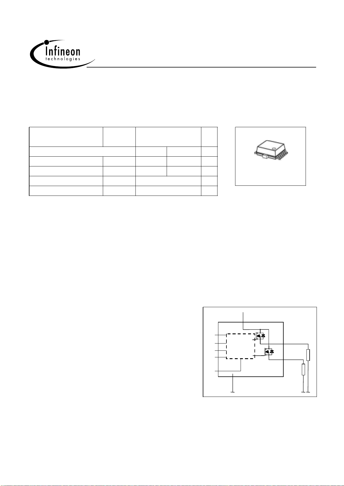
Smart High-Side Power Switch
)
)
Two Channels: 2 x 25mΩ
IntelliSense
PCN 2004-018-A: BTS 5240L
Product Summary
Operating voltage V
Active channels one two parallel
On-state resistance R
Nominal load current I
Current limitation Low I
High 40
bb(on)
ON
L(nom
L(SCr
4,5...28
( Loaddump: 40 V )
25 13 mΩ
6 9,1 A
10 A
V
Package
P-DSO-12-2
General Description
• N channel vertical power MOSFET with charge pump, ground referenced CMOS compatible input and
diagnostic feedback, monolithically integrated in Smart SIPMOS
• Providing embedded protective functions.
• Extern adjustable current limitation.
technology.
Application
• All types of resistive, inductive and capacitive loads
• µC compatible high-side power switch with diagnostic feedback for 12 V grounded loads
• Due to the adjustable current limitation best suitable for loads with high inrush currents, so as lamps
• Replaces electromechanical relays, fuses and discrete circuits
Basic Functions
• Very low standby current
• CMOS compatible input
• Improved electromagnetic compatibility (EMC)
• Stable behaviour at low battery voltage
Protection Functions
• Reverse battery protection with external resistor
• Short circuit protection
• Overload protection
• Current limitation
• Thermal Shutdown
• Overvoltage protection with external resistor
• Loss of GND and loss of V
• Electrostatic discharge Protection (ESD)
protection
bb
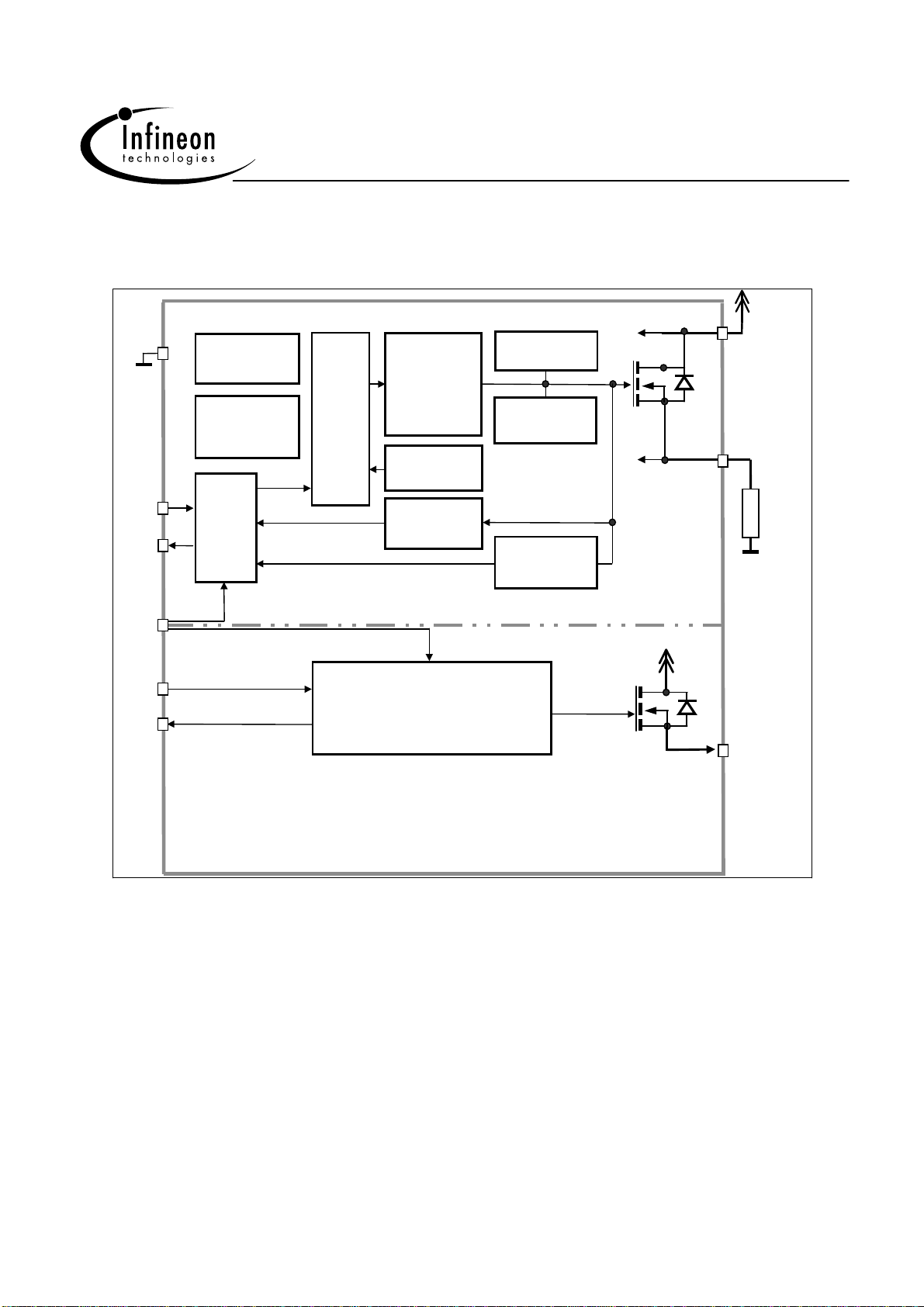
Block Diagram
Vbb
IN1
IS1
IN2
IS2
CLA
Logic
Channel 1
Channel 2
GND
Diagnostic Function: IntelliSense
• Proportional load current sense ( with defined fault signal during thermal shutdown and overload )
• Additional open load detection in OFF - state
• Suppressed thermal toggling of fault signal
Load 1
Load 2
Page 1
2004-Mar-08
Functional diagram
PCN 2004-018-A: BTS 5240L
GND
IN1
IS1
CLA
IN2
IS2
overvoltage
protection
internal
voltage
supply
ESD
gate control
+
charge
pump
logic
temperature
sensor
openload
detection
Channel 1
control and protection circuit
equivalent to
channel 2
current limit
clamp for
inductive load
current
sense
V
OUT1
OUT2
bb
LOAD
Page 2
2004-Mar-08
Pin definition and function
PCN 2004-018-A: BTS 5240L
Pin
2
5
3
4
1
6,12,
heat
slug
7
8,9
10,11
Symbol
IN1
IN2
IS1
IS2
GND
V
bb
CLA
OUT2
OUT1
Function
Input 1,2 activates channel1,2 in case of logic high signal
Diagnostic feedback 1 & 2 of channel 1,2
On state: advanced current sense with defined signal in case
of overload or short circuit
Off state: High on failure
Ground of chip
Positive power supply voltage. Design the wiring for the
simultaneous max. short circuit currents from channel 1 to 2 and
also for low thermal resistance
Current limit adjust, the current limit for both channels can be
chosen as high ( potential < 2,6V ) or low ( potential > 3,6V ).
Output 1,2 protected high-side power output of channel 1,2.
Design the wiring for the max. short circuit current.
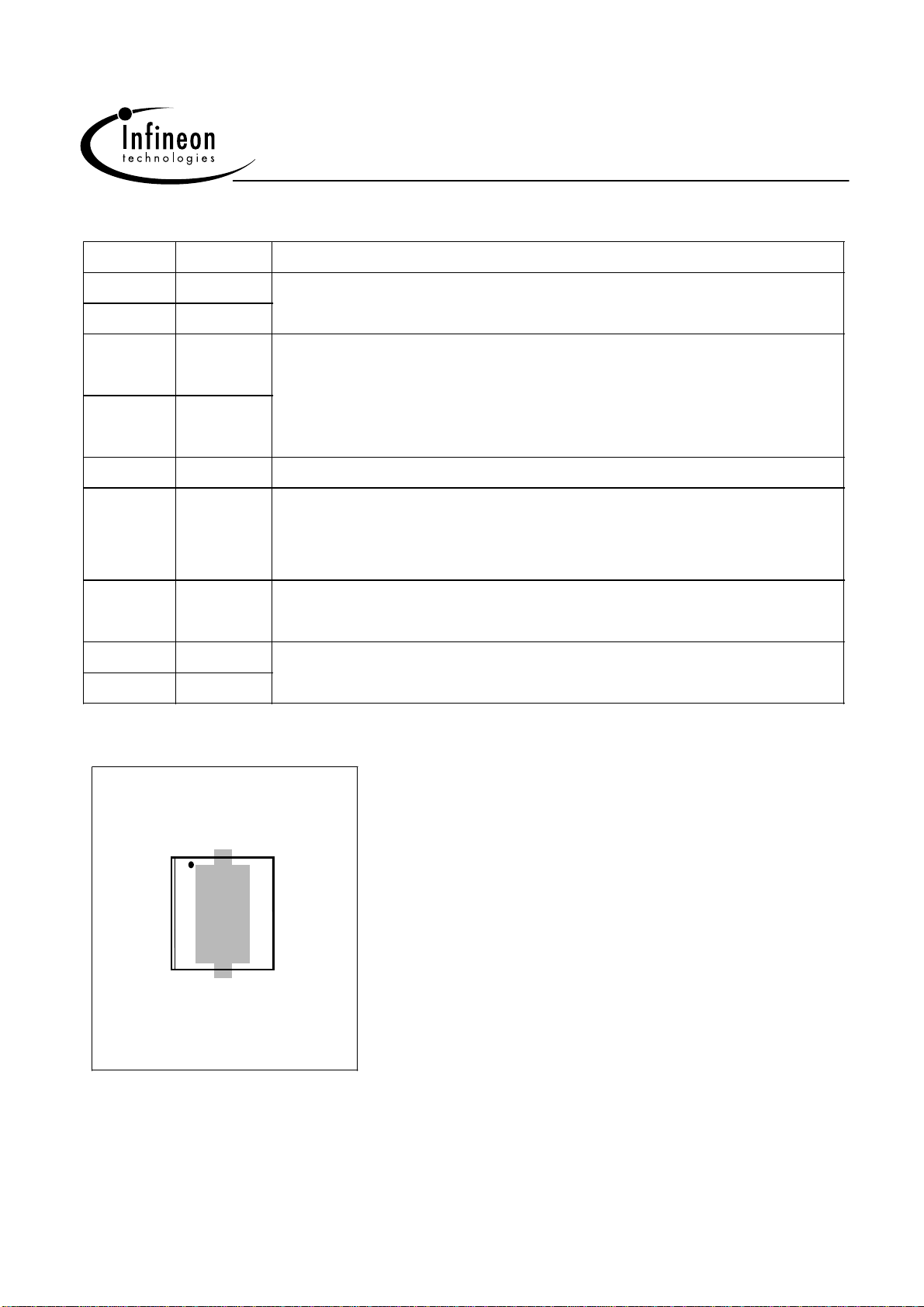
Pin configuration
(top vi ew)
GND 1 12 V
IN1 2 11 OUT1
IS1 3 10 OUT1
IS2 4 9 OUT2
IN2 5 8 OUT2
Vbb67 CLA
* heat slug
*
V
bb
bb
Page 3
2004-Mar-08

PCN 2004-018-A: BTS 5240L
)
)
g
A
A
A
Maximum Ratings at Tj=25°C, unless otherwise specified
Parameter Symbol Value Unit
Supply voltage (overvoltage protection see page 6) V
Supply voltage for full short circuit protection; Tj = -40...150°C V
Maximum voltage across DMOS V
Load dump protection3) V
LoadDump
In = low or high; td = 400 ms; R
R
= 2.25 Ω
L
R
= 6.8 Ω
L
4)
= VA + VS; VA = 13,5 V
4)
= 2 Ω
I
V
Load current (Short - circuit current, see page 7) I
Operating temperature range T
Storage temperature range T
bb
bb(SC
ON
Loaddump
L
j
st
1)
28
2)
28
52
40
53
5)
I
L(lim
-40...+150
-55...+150
Dynamical temperature rise at switching dT 60 K
V
A
°C
Power dissipation6) (DC), one channel active TA = 85 °C
Maximal switchable inductance, single pulse
Vbb=12V, T
IL = 6 A, EAS = 0.319 J, R
IL = 12 A, E
=150°C; (see diagrams on page 12)
jstart
= 0 Ω, one channel:
L
= 0.679 J, R
S
= 0 Ω, two parallel channels:
L
Electrostatic discharge voltage IN:
(Human Body Model) IS:
according to ANSI EOS/ESD - S5.1 - 1993 , ESD STM5.1 - 1998 OUT:
Continuous input voltage V
Voltage at current limit adjustment pin V
Current through current limit adjustment pin I
Current through input pin (DC) I
Current through sense (DC) (see page 11) I
1
18...28 V for 100 hours
2
only single pulse,
line, contact and generator impedances.
3
Supply voltage higher than
4
R
= internal resistance of the load dump test pulse generator.
I
5
Current limit is a protection function. Operation in current limitation is considered as "outside" normal operating
range. Protection functions are not designed for continuous repetitive operation.
6
Device on 50mm*50mm*1.5mm epoxy PCB FR4 with 6 cm2 (one layer, 70µm thick) copper area for Vbb
connection. PCB is vertical without blown air.
R
= 200 m
L
Ω ; L = 8 µH ; R and L are describing the complete circuit impedance including
V
bb(AZ)
require an external current limit for the GND(150
P
Z
V
CL
IN
IS
tot
L(s)
ESD
IN
CL
1,4
9.8
5.2
1.0
2.0
4.0
-10...16 V
-10...16
±5.0
±5.0
-5...+10
Ω resistor) and sense pin.
W
mH
kV
mA
Page 4
2004-Mar-08

PCN 2004-018-A: BTS 5240L
Electrical Characteristics
Parameter and Conditions, each of the two channels Symbol Values Unit
at Tj = -40...+150 °C, Vbb = 9...16 V, unless otherwise specified min. typ. max.
Thermal Resistance
junction - case each channe
junction - ambient1) one channel active:
all channels active:
Load Switching Capabilities and Characteristics
On-state resistance (Vbb to OUT), (see page 13)
T
= 25 °C, IL = 5 A, each channel:
j
T
= 150 °C, each channel:
j
T
= 25 °C, two parallel channels:
j
Nominal load current1)
Ta = 85°C, T
≤ 150°C , one channel active:
j
two channels active, per channel:
Nominal load current; ISO Norm
T
= 85 °C, VON = 0.5 V, one channel active:
C
two channels active, per channel:
Output voltage drop limitation at small load currents
IL = 0.5 A
R
thJC
R
thJA
R
ON
I
L(nom)
I
L(ISO)
V
ON(NL)
- - 1.8 K/W
-
-
-
-
-
5.5
4.1
13
13
40
33
21
42
11
6
4.5
15
15
-
-
25
50
13
-
-
-
-
K/W
mΩ
A
- 40 - mV
Output current while GND disconnected
( see diagram page 12 )
2)
I
L(GNDhigh)
- - 2 mA
VIN = 0 V
1
Device on 50mm*50mm*1.5mm epoxy PCB FR4 with 6 cm2 (one layer, 70µm thick) copper area for Vbb
connection. PCB is vertical without blown air.
2
not subject to production test, specified by design
Page 5
2004-Mar-08
 Loading...