

INFINEON BTS 5234G User Manual

现货库存、技术资料、百科信息、热点资讯,精彩尽在鼎好!
Data Sheet, V1.0, January 2004
BTS 5234G
Smart High-Side Power Switch
PROFET
Two Channels, 60 mΩ
Automotive Power
Never stop thinking.

Smart High-Side Power Switch
BTS 5234G
Table of Contents Page
Product Summary . . . . . . . . . . . . . . . . . . . . . . . . . . . . . . . . . . . . . . . . . . . . . . . . . . . .3
1Overview . . . . . . . . . . . . . . . . . . . . . . . . . . . . . . . . . . . . . . . . . . . . . . . . . . . . . . . . .5
1.1 Block Diagram . . . . . . . . . . . . . . . . . . . . . . . . . . . . . . . . . . . . . . . . . . . . . . . . . . .5
1.2 Terms . . . . . . . . . . . . . . . . . . . . . . . . . . . . . . . . . . . . . . . . . . . . . . . . . . . . . . . . .6
2 Pin Configuration . . . . . . . . . . . . . . . . . . . . . . . . . . . . . . . . . . . . . . . . . . . . . . . . . .7
2.1 Pin Assignment BTS 5234G . . . . . . . . . . . . . . . . . . . . . . . . . . . . . . . . . . . . . . . .7
2.2 Pin Definitions and Functions . . . . . . . . . . . . . . . . . . . . . . . . . . . . . . . . . . . . . . .7
3 Electrical Characteristics . . . . . . . . . . . . . . . . . . . . . . . . . . . . . . . . . . . . . . . . . . . .8
3.1 Maximum Ratings . . . . . . . . . . . . . . . . . . . . . . . . . . . . . . . . . . . . . . . . . . . . . . . .8
4 Block Description and Electrical Characteristics . . . . . . . . . . . . . . . . . . . . . . .10
4.1 Power Stages . . . . . . . . . . . . . . . . . . . . . . . . . . . . . . . . . . . . . . . . . . . . . . . . . .10
4.1.1 Output On-State Resistance . . . . . . . . . . . . . . . . . . . . . . . . . . . . . . . . . . 10
4.1.2 Input Circuit . . . . . . . . . . . . . . . . . . . . . . . . . . . . . . . . . . . . . . . . . . . . . . . 10
4.1.3 Inductive Output Clamp . . . . . . . . . . . . . . . . . . . . . . . . . . . . . . . . . . . . . . 11
4.1.4 Electrical Characteristics . . . . . . . . . . . . . . . . . . . . . . . . . . . . . . . . . . . . 13
4.2 Protection Functions . . . . . . . . . . . . . . . . . . . . . . . . . . . . . . . . . . . . . . . . . . . . .15
4.2.1 Over Load Protection . . . . . . . . . . . . . . . . . . . . . . . . . . . . . . . . . . . . . . . . 15
4.2.2 Reverse Polarity Protection . . . . . . . . . . . . . . . . . . . . . . . . . . . . . . . . . . . 16
4.2.3 Over Voltage Protection . . . . . . . . . . . . . . . . . . . . . . . . . . . . . . . . . . . . . 16
4.2.4 Loss of Ground Protection . . . . . . . . . . . . . . . . . . . . . . . . . . . . . . . . . . . . 16
4.2.5 Electrical Characteristics . . . . . . . . . . . . . . . . . . . . . . . . . . . . . . . . . . . . 17
4.3 Diagnosis . . . . . . . . . . . . . . . . . . . . . . . . . . . . . . . . . . . . . . . . . . . . . . . . . . . . . .18
4.3.1 ON-State Diagnosis . . . . . . . . . . . . . . . . . . . . . . . . . . . . . . . . . . . . . . . . . 19
4.3.2 OFF-State Diagnosis . . . . . . . . . . . . . . . . . . . . . . . . . . . . . . . . . . . . . . . . 20
4.3.3 Sense Enable Function . . . . . . . . . . . . . . . . . . . . . . . . . . . . . . . . . . . . . . 21
4.3.4 Electrical Characteristics . . . . . . . . . . . . . . . . . . . . . . . . . . . . . . . . . . . . 22
5 Package Outlines BTS 5234G . . . . . . . . . . . . . . . . . . . . . . . . . . . . . . . . . . . . . . .24
6 Revision History . . . . . . . . . . . . . . . . . . . . . . . . . . . . . . . . . . . . . . . . . . . . . . . . . .25
Data Sheet 2 V1.0, 2004-01-23
Smart High-Side Power Switch
PROFET
Product Summary
The BTS 5234G is a dual channel high-side power
switch in P-DSO-20-21 package providing embedded
protective functions.
The power transistor is built by a N-channel vertical
power MOSFET with charge pump. The device is
monolithically integrated in Smart SIPMOS
technology.
Operating voltage
V
bb(on)
BTS 5234G
P-DSO-20-21
4.5..28V
Over voltage protection
On-State resistance
Nominal load current (one channel active)
Current limitation
Current limitation repetitive
Standby current for whole device with load
V
bb(AZ)
R
DS(ON)
I
L(nom)
I
L(LIM)
I
L(SCr)
I
bb(OFF)
Basic Features
• Very low standby current
• 3.3 V and 5 V compatible logic pins
• Improved electromagnetic compatibility (EMC)
• Stable behavior at under voltage
• Logic ground independent from load ground
• Secure load turn-off while logic ground disconnected
• Optimized inverse current capability
41 V
60 mΩ
3.3 A
23 A
6A
2.5 µA
Type Ordering Code Package
BTS 5234G Q67060-S6156 P-DSO-20-21
Data Sheet 3 V1.0, 2004-01-23

Smart High-Side Power Switch
Protective Functions
• Reverse battery protection without external components
• Short circuit protection
• Overload protection
• Multi-step current limitation
• Thermal shutdown with restart
• Thermal restart at reduced current limitation
• Over voltage protection without external resistor
• Loss of ground protection
• Electrostatic discharge protection (ESD)
Diagnostic Functions
• Enhanced IntelliSense signal for each channel
• Enable function for diagnosis pins (IS1 and IS2)
• Proportional load current sense signal by current source
• High accuracy of current sense signal at wide load current range
• Open load detection in ON-state by load current sense
• Open load detection in OFF-state by voltage source
• Feedback on over temperature and current limitation in ON-state
BTS 5234G
Applications
• µC compatible high-side power switch with diagnostic feedback for 12 V grounded
loads
• All types of resistive, inductive and capacitive loads
• Suitable for loads with high inrush currents, so as lamps
• Suitable for loads with low currents, so as LEDs
• Replaces electromechanical relays, fuses and discrete circuits
Data Sheet 4 V1.0, 2004-01-23
Smart High-Side Power Switch
BTS 5234G
Overview
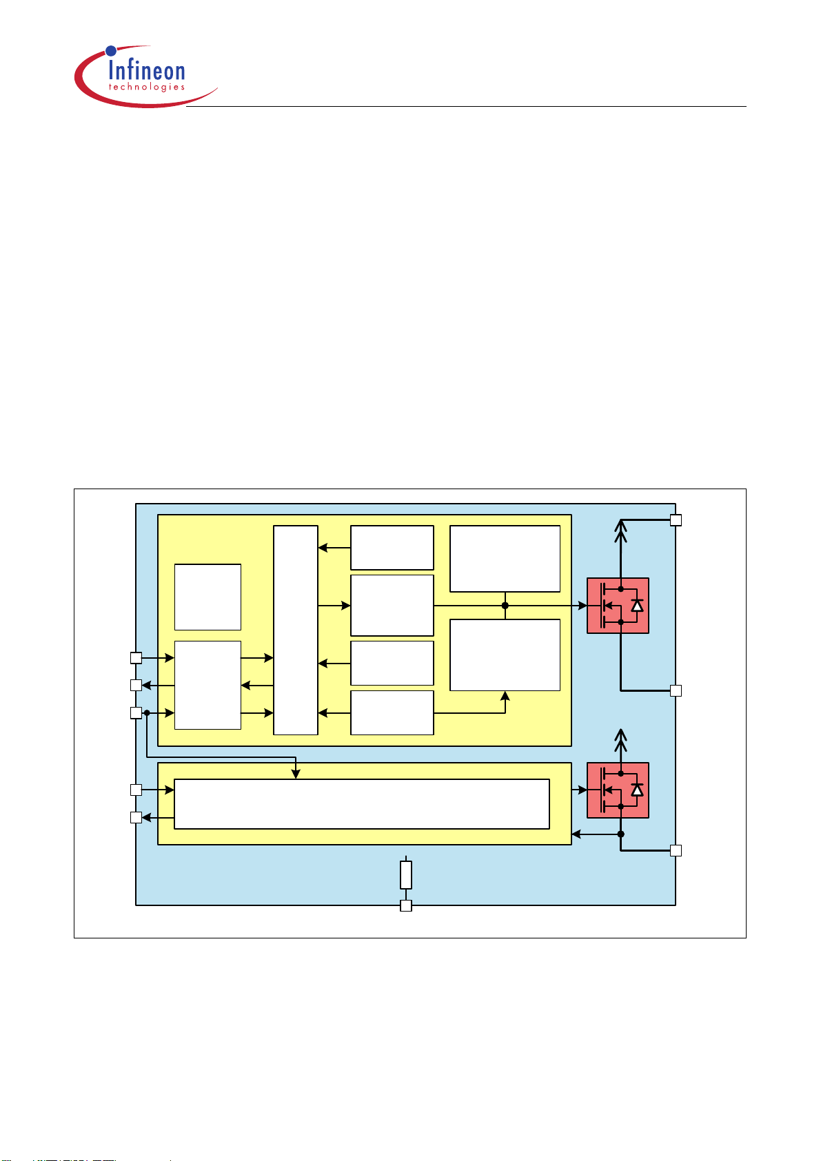
1Overview
The BTS 5234G is a dual channel high-side power switch (two times 60 mΩ) in
P-DSO-20-21 package providing embedded protective functions.
The Enhanced IntelliSense pins IS1 and IS2 provide a sophisticated diagnostic feedback
signal including current sense function and open load in off state. The diagnosis signals
can be switched on and off by the sense enable pin SEN.
An integrated ground resistor as well as integrated resistors at each input pin (IN1, IN2,
SEN) reduce external components to a minimum.
The power transistor is built by a N-channel vertical power MOSFET with charge pump.
The inputs are ground referenced CMOS compatible. The device is monolithically
integrated in Smart SIPMOS technology.
1.1 Block Diagram
VBB
OUT1
IN1
IS1
SEN
channel 1
internal
power
supply
ESD
protection
logic
load cur rent
sense
gate control
&
char ge pum p
open l oad
detection
tem per atur e
sensor
clamp for
inductive load
multi step
load cur r ent
limitation
channel 2
IN2
IS2
control and protecti on cir cuit
equival ent to
channel 1
R
GND
GND
OUT2
Figure 1 Block Diagram
Data Sheet 5 V1.0, 2004-01-23
Smart High-Side Power Switch
BTS 5234G
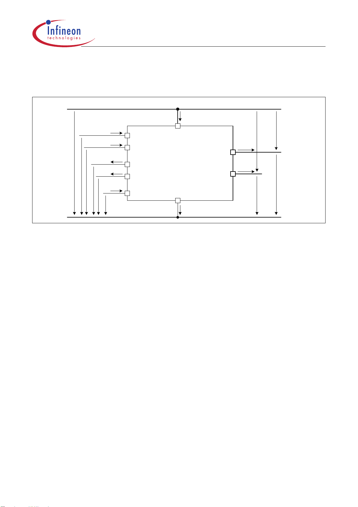
1.2 Terms
Following figure shows all terms used in this data sheet.
V
bb
I
IN1
IN1
V
IN1
V
IN2
I
IN2
IN2
I
IS1
BTS 5234G
IS1
I
V
IS1
IS2
IS2
V
IS2
I
SEN
SEN
V
SEN
VBB
GND
I
bb
I
GND
OUT1
OUT2
Overview
I
L1
I
L2
V
V
V
V
OUT1
DS2
OUT2
DS1
Ter m s2 ch . em f
Figure 2 Terms
Data Sheet 6 V1.0, 2004-01-23
Smart High-Side Power Switch
BTS 5234G
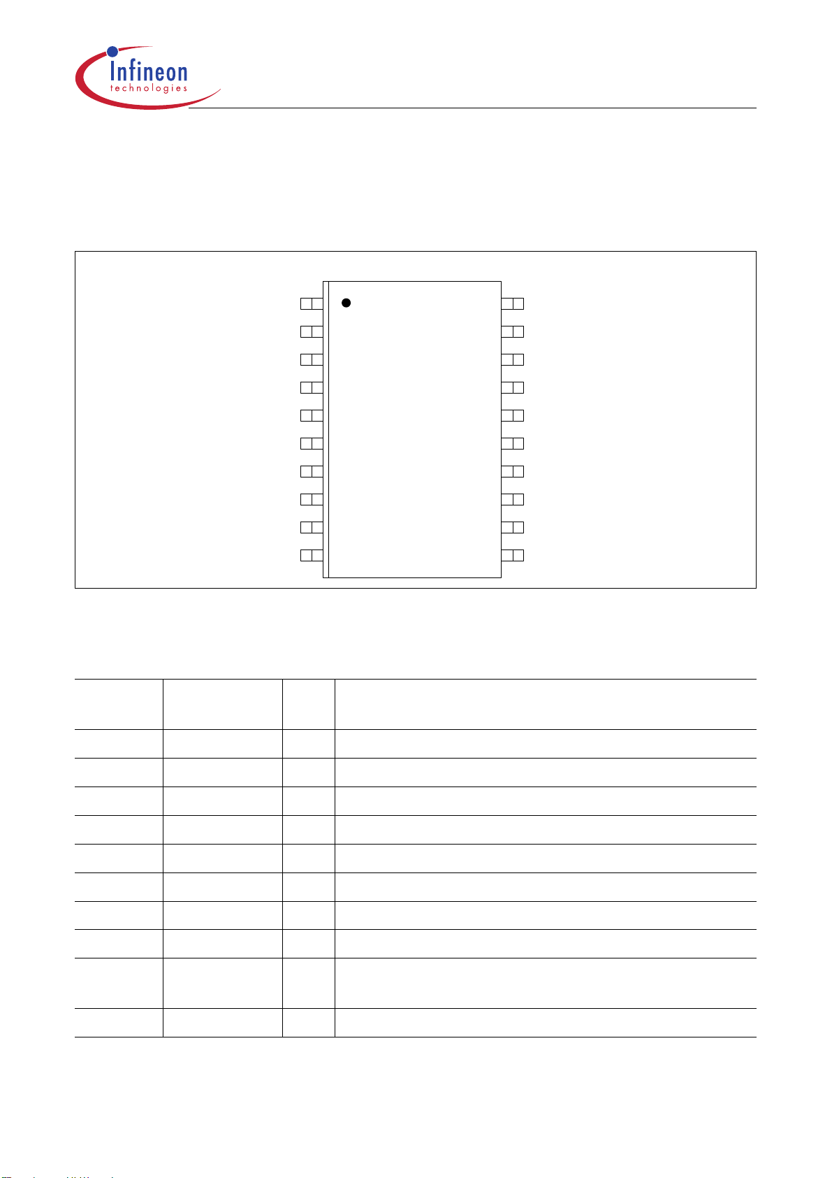
2 Pin Configuration
2.1 Pin Assignment BTS 5234G
(top view)
VBB
nc
GND
IN1
IS1
IS2
IN2
SEN
nc
1
2
3
4
5
6
7
8
9
20
19
18
17
16
15
14
13
12
Pin Configuration
VBB
OUT1
OUT1
OUT1
VBB
VBB
OUT2
OUT2
OUT2
VBB
10
11
VBB
Figure 3 Pin Configuration P-DSO-20-21
2.2 Pin Definitions and Functions
Pin Symbol I/O
OD
4 IN1 I Input signal for channel 1
7 IN2 I Input signal for channel 2
5 IS1 O Diagnosis output signal channel 1
6 IS2 O Diagnosis output signal channel 2
8 SEN I Sense Enable input for channel 1&2
17, 18 ,19 OUT1 O Protected high-side power output channel 1
12, 13, 14 OUT2 O Protected high-side power output channel 2
3 GND - Ground connection
Function
1, 10, 11,
20
VBB - Positive power supply for logic supply as well as
output power supply
2, 9 nc - not connected
Data Sheet 7 V1.0, 2004-01-23
Smart High-Side Power Switch
BTS 5234G
Electrical Characteristics
3 Electrical Characteristics
3.1 Maximum Ratings
Stresses above the ones listed here may affect device reliability or may cause permanent
damage to the device.
Unless otherwise specified:
T
= 25 °C
j
Pos. Parameter Symbol Limit Values Unit Test
Conditions
R = 0.2 Ω
1)
Supply Voltage
3.1.1 Supply voltage V
3.1.2 Supply voltage for full short
V
circuit protection (single pulse)
T
= -40°C .. 150°C)
(
j(0)
bb
bb(SC)
min. max.
-16 28 V
028VL = 8 µH,
3.1.3 Voltage at power transistor V
3.1.4 Supply Voltage for Load Dump
V
protection
Power Stages
3.1.5 Load current
3.1.6 Maximum energy dissipation
I
E
single pulse
3.1.7 Power dissipation (DC)
P
Logic Pins
3.1.8 Voltage at input pin
3.1.9 Current through input pin
3.1.10 Voltage at sense enable pin
V
I
V
DS
bb(LD)
L
AS
tot
IN
IN
SEN
-52V
41 V RI = 2 Ω
R
= 6.8 Ω
L
L(0)
T
3)
j(0)
= 2 A
= 150°C
- I
L(LIM)
A-
-0.58JI
-1.4WTa = 85 °C
T
≤ 150 °C
j
-5
-16
-2.0
-8.0
-5
-16
10 V
t ≤ 2min
2.0 mA
t ≤ 2min
10 V
t ≤ 2min
2)
4)
5)
3.1.11 Current through sense enable
pin
3.1.12 Current through sense pin
Data Sheet 8 V1.0, 2004-01-23
I
SEN
I
IS
-2.0
2.0 mA
-8.0
-25 10 mA
t ≤ 2min
Smart High-Side Power Switch
BTS 5234G
Electrical Characteristics
Unless otherwise specified:
T
= 25 °C
j
Pos. Parameter Symbol Limit Values Unit Test
min. max.
Conditions
Temperatures
3.1.13 Junction Temperature
3.1.14 Dynamic temperature increase
T
j
∆T
-40 150 °C
j
-60°C
while switching
3.1.15 Storage Temperature
T
stg
-55 150 °C
ESD Susceptibility
IS
V
ESD
-1
-2
-4
kV according to
1
2
EIA/JESD
22-A 114B
4
3.1.16 ESD susceptibility HBM
IN, SEN
OUT
1)
R and L describe the complete circuit impedance including line, contact and generator impedances
2)
Load Dump is specified in ISO 7636, RI is the internal resistance of the Load Dump pulse generator
3)
Current limitation is a protection feature. Operation in current limitation is considered as “outside” normal
operating range. Protection features are not designed for continuous repetitive operation.
4)
Pulse shape represents inductive switch off: I
5)
Device mounted on PCB (50 mm x 50 mm x 1.5mm epoxy, FR4) with 6 cm2 copper heatsinking area (one
layer, 70 µm thick) for V
connection. PCB is vertical without blown air.
bb
(t) = IL(0) * (1 - t / t
L
); 0 < t < t
peak
peak
Data Sheet 9 V1.0, 2004-01-23
 Loading...