

现货库存、技术资料、百科信息、热点资讯,精彩尽在鼎好!
)
)
)
Smart Power High-Side-Switch
BTS 452 R
Features
• Overload protection
• Current limitation
• Short circuit protection
• Thermal shutdown with restart
Product Summary
Overvoltage protection V
Operating voltage V
On-state resistance R
Nominal load current I
• Overvoltage protection
(including load dump)
• Fast demagnetization of inductive loads
• Reverse battery protection
with external resistor
• Open drain diagnostic output for overtemperature
and short circuit
• Open load detection in OFF - State
with external resistor
• CMOS compatible input
bb(AZ
bb(on
ON
L(ISO
62 V
6...52 V
200 mΩ
1.8 A
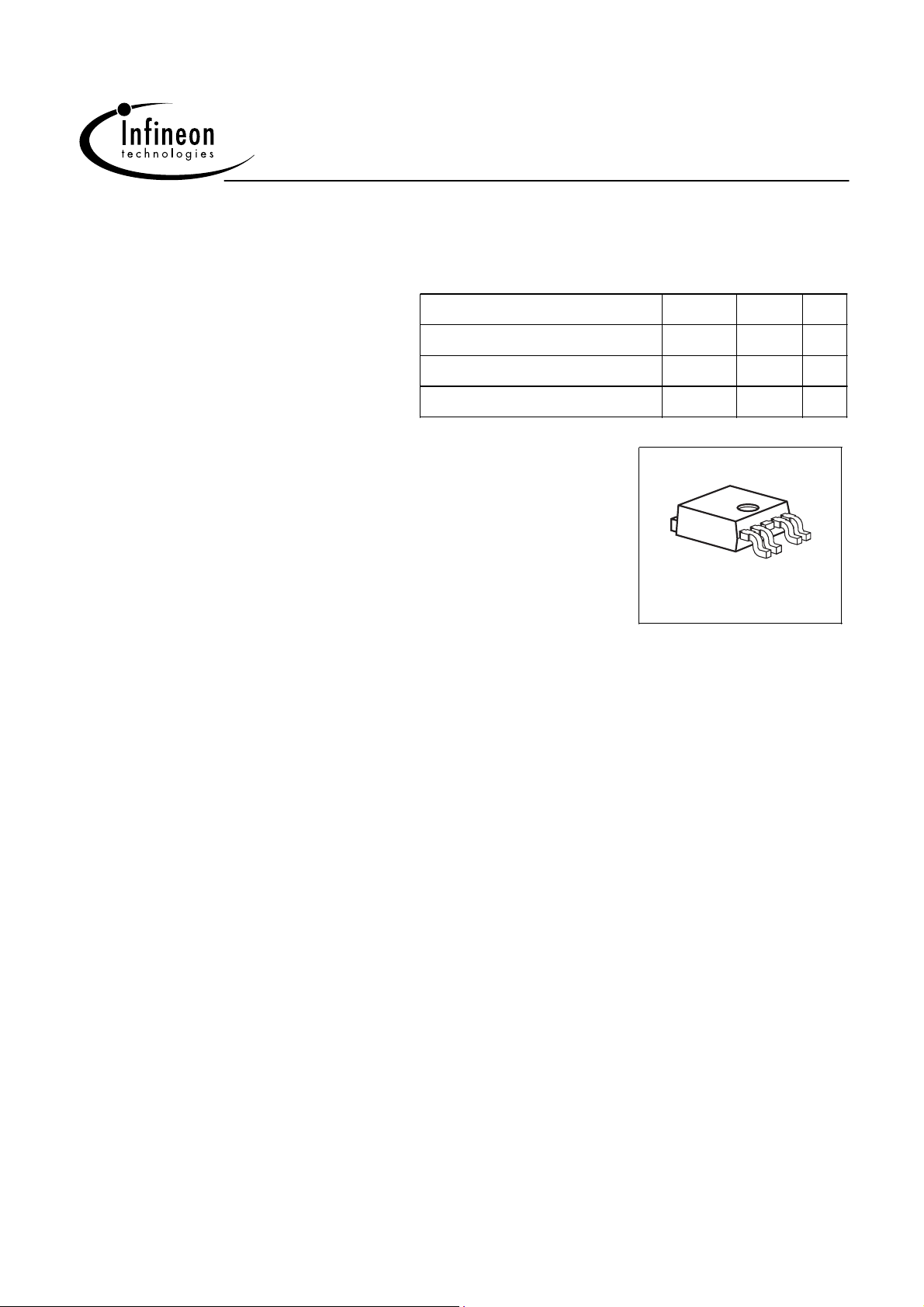
P-TO252-5-11
• Loss of GND and loss of V
protection
bb
• ESD - Protection
• Very low standby current
Application
• All types of resistive, inductive and capacitive loads
• µC compatible power switch for 12 V, 24 V and 42 V DC applications
• Replaces electromechanical relays and discrete circuits
General Description
N channel vertical power FET with charge pump, ground referenced CMOS compatible input
and diagnostic feedback, monolithically integrated in Smart SIPMOS technology.
Providing embedded protective functions.
Page 1
2004-01-27
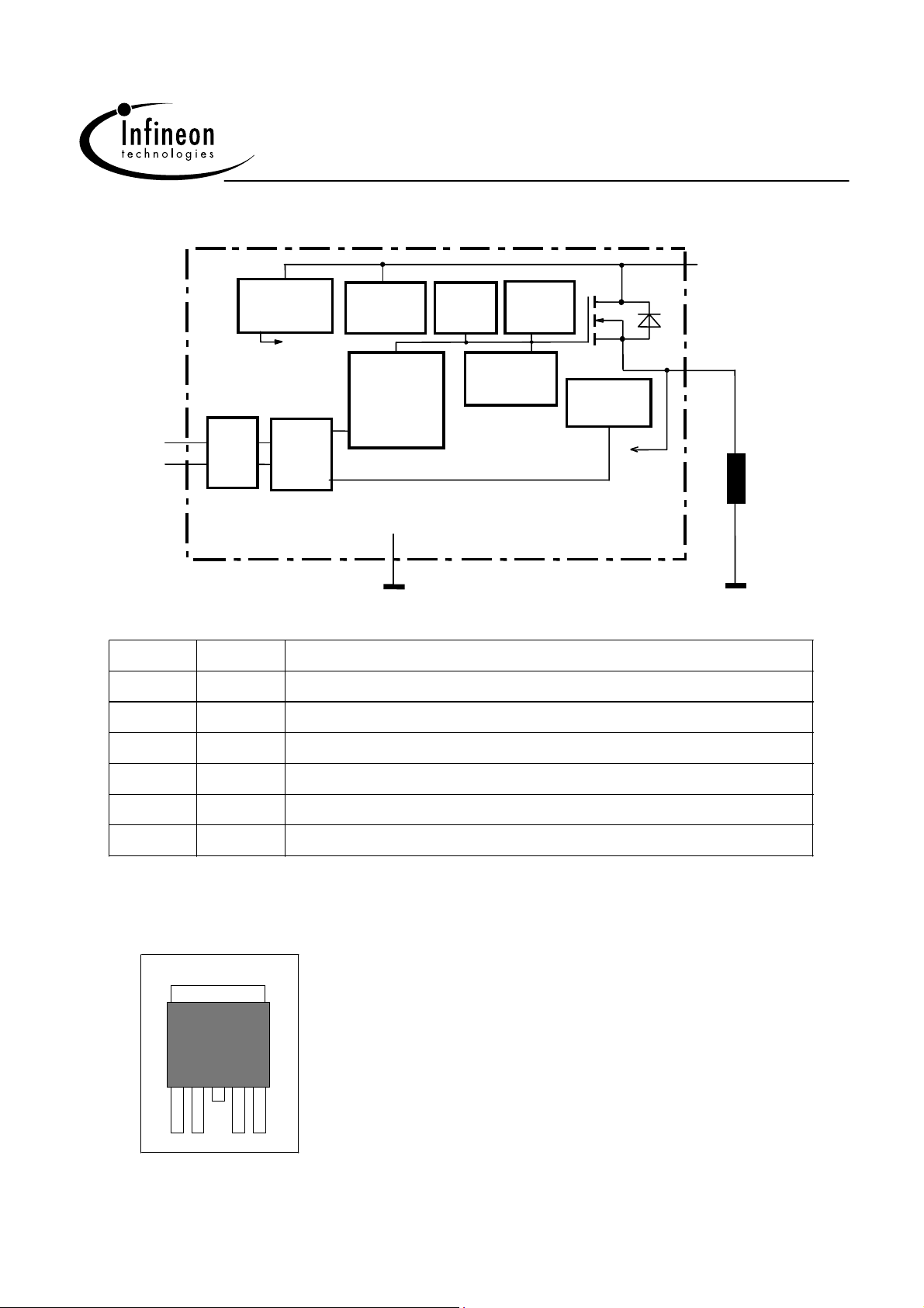
Block Diagram
IN
ESD
ST
Voltage
source
V
Logic
Logic
Overvoltage
protection
Charge pump
Level shifter
Rectifier
Current
limit
Gate
protection
Limit for
unclamped
ind. loads
Temperature
sensor
+ V
BTS 452 R
bb
OUT
Load
GND
Signal GND
miniPROFET
Pin Symbol Function
1
2
3
4
5
GND Logic ground
IN Input, activates the power switch in case of logic high signal
Vbb Positive power supply voltage
ST Diagnostic feedback
OUT Output to the load
TAB Vbb Positive power supply voltage
Pin configuration
Top view
Load GND
Tab = V
BB
1 2 (3) 4 5
GND IN ST OUT
Page 2
2004-01-27

BTS 452 R
)
)
)
Maximum Ratings at Tj = 25°C, unless otherwise specified
Parameter Symbol Value Unit
Supply voltage V
Supply voltage for full short circuit protection V
Continuous input voltage V
Load current (Short - circuit current, see page 5) I
Current through input pin (DC) I
Operating temperature T
Storage temperature T
Power dissipation
1)
Inductive load switch-off energy dissipation
1)2)
P
E
single pulse, (see page 9)
Tj =150 °C, IL = 1 A
Load dump protection2) V
R
=2Ω, t
I
R
= 13.5 Ω
L
R
= 27 Ω
L
=400ms, VIN= low or high, VA=13,5V
d
LoadDump
3)
= VA + V
V
S
bb
bb(SC
IN
L
IN
j
stg
tot
AS
Loaddump
52 V
50
-10 ... +16
self limited A
± 5
-40 ...+150
-55 ... +150
41.6 W
150 mJ
73.5
88.5
mA
°C
V
Electrostatic discharge voltage (Human Body Model)
V
ESD
according to ANSI EOS/ESD - S5.1 - 1993
ESD STM5.1 - 1998
Input pin
all other pins
Thermal Characteristics
junction - case:
Thermal resistance @ min. footprint R
Thermal resistance @ 6 cm2 cooling area
1
Device on 50mm*50mm*1.5mm epoxy PCB FR4 with 6 cm2 (one layer, 70µm thick) copper area for drain
connection. PCB is vertical without blown air. (see page 17)
2
not subject to production test, specified by design
3
V
Loaddump
Supply voltages higher than V
150Ω resistor in GND connection. A resistor for the protection of the input is integrated.
is setup without the DUT connected to the generator per ISO 7637-1 and DIN 40839 .
require an external current limit for the GND pin, e.g. with a
bb(AZ)
1)
R
R
thJC
th(JA
th(JA
- - 3 K/W
- 80 - K/W
- 45 60
kV
± 1
± 5
Page 3
2004-01-27

BTS 452 R
)
p)
Electrical Characteristics
Parameter and Conditions Symbol Values Unit
at Tj = -40...+150°C, V
= 12..42V, unless otherwise specified min. typ. max.
bb
Load Switching Capabilities and Characteristics
On-state resistance
T
= 25 °C, IL = 1 A, Vbb = 9...52 V
j
T
= 150 °C
j
Nominal load current; Device on PCB 1)
T
= 85 °C, VON = 0.5 V
C
Turn-on time to 90% V
R
= 47 Ω
L
Turn-off time to 10% V
R
= 47 Ω
L
Slew rate on 10 to 30% V
R
= 47 Ω, V
L
= 13.5 V
bb
Slew rate off 70 to 40% V
R
= 47 Ω, V
L
= 13.5 V
bb
OUT
OUT
OUT
OUT
,
,
R
ON
I
L(ISO)
t
on
t
off
dV/dt
-dV/dt
on
off
-
-
150
270
200
380
mΩ
1.8 2.2 - A
- 80 180
µs
- 80 200
- 0.7 2
V/µs
- 0.9 2
Operating Parameters
Operating voltage V
Undervoltage shutdown of charge pump
T
= -40...+85 °C
j
T
= 150 °C
j
Undervoltage restart of charge pump V
Standby current
T
= -40...+85 °C, VIN = low
j
Tj = +150 °C 2), VIN = low
Leakage output current (included in I
bb(off)
)
bb(on
V
bb(under)
bb(u c
I
bb(off)
I
L(off)
6 - 52 V
-
-
- 4 5.5
-
-
- - 5
VIN = low
Operating current
I
GND
- 0.8 2 mA
VIN = high
1
Device on 50mm*50mm*1.5mm epoxy PCB FR4 with 6 cm2 (one layer, 70µm thick) copper area for drain
connection. PCB is vertical without blown air. (see page 17)
2
higher current due temperature sensor
-
-
-
-
4
5.5
15
18
µA
Page 4
2004-01-27

BTS 452 R
j
j
Electrical Characteristics
Parameter and Conditions Symbol Values Unit
at Tj = -40...+150°C, V
Protection Functions
= 12..42V, unless otherwise specified min. typ. max.
bb
1)
Initial peak short circuit current limit (pin 3 to 5)
T
= -40 °C, Vbb = 20 V, tm = 150 µs
j
T
= 25 °C
j
T
= 150 °C
j
T
= -40...+150 °C, Vbb > 40 V , ( see page 12 )
j
Repetitive short circuit current limit
Tj = Tjt (see timing diagrams)
Vbb < 40V
Vbb > 40V
Output clamp (inductive load switch off)
at V
= Vbb - V
OUT
ON(CL)
,
Ibb = 4 mA
Overvoltage protection 3)
Ibb = 4 mA
I
L(SCp)
I
L(SCr)
V
ON(CL)
V
bb(AZ)
-
-
4
-
-
-
-
6.5
-
52)
6
4.5
A
9
-
-
-
-
-
59 63 - V
62 - -
Thermal overload trip temperature T
Thermal hysteresis ∆T
t
t
150 - - °C
- 10 - K
Reverse Battery
Reverse battery
Drain-source diode voltage (V
T
= 150 °C
j
1
Integrated protection functions are designed to prevent IC destruction under fault conditions
described in the data sheet. Fault conditions are considered as "outside" normal operating range.
Protection functions are not designed for continuous repetitive operation .
2
not subject to production test, specified by design
3
see also V
4
Requires a 150 Ω resistor in GND connection. The reverse load current through the intrinsic drain-source diode has
to be limited by the connected load. Power dissipation is higher compared to normal operating conditions due to the
voltage drop across the drain-source diode. The temperature protection is not active during reverse current operation!
Input current has to be limited (see max. ratings page 3).
ON(CL)
4)
OUT
in circuit diagram on page 8
> Vbb)
-V
-V
bb
ON
- - 52 V
- 600 - mV
Page 5
2004-01-27

BTS 452 R
)
)
)
)
)
)
Electrical Characteristics
Parameter and Conditions Symbol Values Unit
at Tj = -40...+150°C, V
= 12..42V, unless otherwise specified min. typ. max.
bb
Input and Status feedback
Input turn-on threshold voltage V
Input turn-off threshold voltage V
Input threshold hysteresis ∆V
Off state input current
I
IN(off)
VIN = 0.7 V
On state input current
I
IN(on)
VIN = 5 V
Status output (open drain), Zener limit voltage
V
IST = 1.6 mA
Status output (open drain), ST low voltage
T
= -40...+25 °C, IST = 1.6 mA
j
T
= 150 °C, IST = 1.6 mA
j
Status invalid after positive input slope 1)
V
t
d(ST+)
Vbb = 20 V
IN(T+
IN(T-
IN(T
ST(high)
ST(low)
- - 2.2 V
0.8 - -
- 0.4 -
1 - 25 µA
3 - 25
5.4 6.1 - V
-
-
-
-
0.4
0.6
- 120 160 µs
Status invalid after negative input slope
1)
t
Input resistance (see page 8) R
Diagnostic Characteristics
Short circuit detection voltage V
3)
2)
V
R
Open load detection voltage
Internal output pull down
( see page 9 and 14 )
V
OUT(OL)
1
no delay time after overtemperature switch off and short circuit in on-state
2
External pull up resistor required for open load detection in off state.
3
not subject to production test, specified by design
= 4 V
d(ST-
I
OUT(SC
OUT(OL
O
- 250 400
2 3.5 5 kΩ
- 2.8 - V
- 3 4
65 200 750 kΩ
Page 6
2004-01-27
 Loading...