

现货库存、技术资料、百科信息、热点资讯,精彩尽在鼎好!
PROFET
Smart Highside Power Switch
®
BTS 442 E2
Features
•
Overload protection
•
Current limitation
•
Short-circuit protection
•
Thermal shutdown
•
Overvoltage protection (including load dump)
•
Fast demagnetization of inductive loads
•
Reverse battery protection
•
Undervoltage and overvoltage shutdown with
auto-restart and hysteresis
•
Open drain diagnostic output
•
Open load detection in ON-state
•
CMOS compatible input
•
Loss of ground and loss of V
•
Electrostatic discharge (ESD) protection
1
)
protection2)
bb
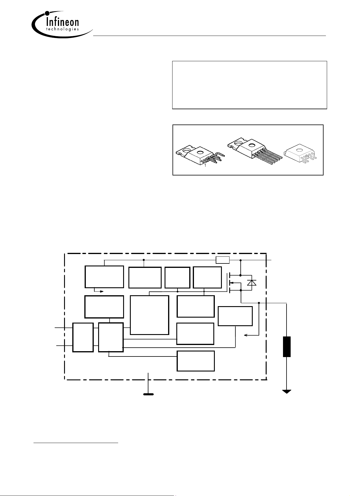
Product Summary
Overvoltage protection V
Operating voltage
V
63 V
bb(AZ)
4.5 ... 42 V
bb(on)
On-state resistance RON 18
Load current (ISO) I
Current limitation I
21 A
L(ISO)
70 A
L(SCr)
TO-220AB/5
5
1
1
SMD
Standard
5
Straight leads
Application
•
µC compatible power switch with diagnostic feedback for 12 V and 24 V DC grounded loads
•
All types of resistive, inductive and capacitve loads
•
Replaces electromechanical relays and discrete circuits
General Description
N channel vertical power FET with charge pump, ground referenced CMOS compatible input and diagnostic
feedback, integrated in Smart SIPMOS
chip on chip technology. Providing embedded protective functions.
mΩ
5
R
Voltage
source
V
Logic
Voltage
sensor
IN
2
ESD
4
ST
Logic
Overvoltage
protection
Charge pump
Level shifter
Rectifier
GND
Current
limit
unclamped
Open load
Short circuit
Gate
protection
Limit for
ind. loads
detection
detection
Temperature
sensor
+ V
bb
PROFET
bb
OUT
3
5
Load
1
Signal GND
Load GND
1)
No external components required, reverse load current limited by connected load.
2)
Additional external diode required for charged inductive loads
Semiconductor Group 1 of 14 2003-Oct-01

BTS 442 E2
Pin Symbol Function
1 GND - Logic ground
2 IN I Input, activates the power switch in case of logical high signal
3 Vbb + Positive power supply voltage,
the tab is shorted to this pin
4 ST S Diagnostic feedback, low on failure
5 OUT
O Output to the load
(Load, L)
Maximum Ratings at Tj = 25 °C unless otherwise specified
Parameter Symbol Values Unit
Supply voltage (overvoltage protection see page 3) Vbb 63 V
3
Load dump protection V
LoadDump
= UA + Vs, UA = 13.5 V
V
Load dump
)
80 V
RI= 2 Ω, RL= 1.1 Ω, td= 200 ms, IN= low or high
Load current (Short-circuit current, see page 4) IL self-limited A
Operating temperature range
Storage temperature range
Power dissipation (DC) P
Tj
T
stg
167 W
tot
-40 ...+150
-55 ...+150
°C
Inductive load switch-off energy dissipation,
single pulse Tj=150 °C: EAS 2.1 J
Electrostatic discharge capability (ESD)
V
2.0 kV
ESD
(Human Body Model)
Input voltage (DC) VIN -0.5 ... +6 V
Current through input pin (DC)
Current through status pin (DC)
see internal circuit diagrams page 6...
Thermal resistance chip - case:
junction - ambient (free air):
I
IN
IST
R
thJC
R
thJA
±5.0
mA
±5.0
≤ 0.75
≤ 75
K/W
SMD version, device on pcb4): ≤ tbd
3)
V
Load dump
4)
Device on 50mm*50mm*1.5mm epoxy PCB FR4 with 6cm
connection. PCB is vertical without blown air.
is setup without the DUT connected to the generator per ISO 7637-1 and DIN 40839
2
(one layer, 70µm thick) copper area for Vbb
Semiconductor Group 2 2003-Oct-01

BTS 442 E2
Electrical Characteristics
Parameter and Conditions Symbol Values Unit
at Tj = 25 °C, Vbb = 12 V unless otherwise specified
Load Switching Capabilities and Characteristics
min typ max
On-state resistance (pin 3 to 5)
= 5 A Tj=25 °C:
I
L
T
=150 °C:
j
Nominal load current (pin 3 to 5)
R
ON
I
17 21 -- A
L(ISO)
--
ISO Proposal: VON = 0.5 V, TC = 85 °C
Output current (pin 5) while GND disconnected or
I
L(GNDhigh)
-- -- 1 mA
GND pulled up, VIN= 0, see diagram page 7,
Tj =-40...+150°C
Turn-on time to 90% V
Turn-off time to 10% V
OUT
OUT
:
ton
:
t
off
100
10
RL = 12 Ω, Tj =-40...+150°C
Slew rate on
10 to 30% V
OUT
, R
= 12 Ω, Tj =-40...+150°C
L
Slew rate off
70 to 40% V
, RL = 12 Ω, Tj =-40...+150°C
OUT
Operating Parameters
Operating voltage 5) Tj =-40...+150°C: V
Undervoltage shutdown Tj =-40...+150°C: V
Undervoltage restart Tj =-40...+150°C: V
Undervoltage restart of charge pump
dV /dton 0.2 -- 2 V/µs
-dV/dt
bb(on)
bb(under)
bb(u rst)
V
bb(ucp)
0.4 -- 5 V/µs
off
4.5 -- 42 V
2.4 -- 4.5 V
-- -- 4.5 V
-- 6.5 7.5 V
see diagram page 12 Tj =-40...+150°C:
Undervoltage hysteresis
∆V
bb(under)
= V
bb(u rst)
- V
bb(under)
Overvoltage shutdown Tj =-40...+150°C: V
Overvoltage restart Tj =-40...+150°C: V
Overvoltage hysteresis Tj =-40...+150°C: ∆V
Overvoltage protection
6)
Tj =-40°C:
Ibb=40 mA Tj =25...+150°C:
Standby current (pin 3) Tj=-40...+25°C:
VIN=0 T
Leakage output current (included in I
VIN=0
bb(off)
=150°C:
j
)
Operating current (Pin 1)7), VIN=5 V
∆V
bb(over)
bb(o rst)
V
bb(AZ)
bb(under)
bb(over)
-- 0.2 -- V
42 -- 52 V
42 -- -- V
-- 0.2 -- V
60
63
I
--
bb(off)
--
I
-- 6 -- µA
L(off)
I
-- 1.1 -- mA
GND
15
28
--
--
--
67
12
18
18
mΩ
35
350
µs
130
-- V
25
µA
60
5)
At supply voltage increase up to V
6)
see also V
7)
Add I
, if IST > 0, add IIN, if VIN>5.5 V
ST
in table of protection functions and circuit diagram page 7. Meassured without load.
ON(CL)
= 6.5 V typ without charge pump, V
bb
≈Vbb - 2 V
OUT
Semiconductor Group 3 2003-Oct-01

BTS 442 E2
Parameter and Conditions Symbol Values Unit
at Tj = 25 °C, Vbb = 12 V unless otherwise specified
min typ max
Protection Functions8)
Initial peak short circuit current limit (pin 3 to 5)9),
( max 400 µs if VON > V
ON(SC)
)
=-40°C:
Tj
=25°C:
Tj
=+150°C:
Tj
Repetitive short circuit current limit I
I
--
L(SCp)
--
--
45
L(SCr)
95
--
Tj = Tjt (see timing diagrams, page 10) 30 70 -- A
Short circuit shutdown delay after input pos. slope
V
ON
> V
, Tj =-40..+150°C:
ON(SC)
t
d(SC)
80
-- 400 µs
min value valid only, if input "low" time exceeds 30 µs
Output clamp (inductive load switch off)
at V
= Vbb - V
OUT
ON(CL)
IL= 30 mA
,
Short circuit shutdown detection voltage
(pin 3 to 5) V
V
ON(CL)
ON(SC)
--
--
58 -- V
8.3 -- V
Thermal overload trip temperature Tjt 150 -- -- °C
Thermal hysteresis
Inductive load switch-off energy dissipation
T
= 150 °C, single pulse Vbb = 12 V:
j Start
10)
,
Vbb = 24 V:
Reverse battery (pin 3 to 1)
11)
-Vbb -- -- 32 V
∆
Tjt -- 10 -- K
E
AS
E
Load12
E
Load24
-- -- 2.1
Integrated resistor in Vbb line Rbb -- 120 -- Ω
Diagnostic Characteristics
Open load detection current Tj=-40 °C:
(on-condition) Tj=25..150°C:
I
2
L (OL)
2
--
--
1900
1500
140
1.7
1.2
A
--
--
J
mA
ON(CL)
- V
d(SC) max
), see diagram page 8
bb
=400 µs, prior to shutdown
ON(CL)
can be reduced by an additional
GND
* iL(t) dt, approx.
8)
Integrated protection functions are designed to prevent IC destruction under fault conditions described in the
data sheet. Fault conditions are considered as "outside" normal operating range. Protection functions are not
designed for continuous repetitive operation.
9)
Short circuit current limit for max. duration of t
10)
While demagnetizing load inductance, dissipated energy in PROFET is EAS= V
V
2
= 1/
E
AS
11)
Reverse load current (through intrinsic drain-source diode) is normally limited by the connected load.
Reverse current I
these condition is dependent on the size of the heatsink. Reverse I
external GND-resistor (150 Ω). Input and Status currents have to be limited (see max. ratings page 2 and
circuit page 7).
* L * I
2
* (
L
V
ON(CL)
of ≈ 0.3 A at Vbb= -32 V through the logic heats up the device. Time allowed under
GND
Semiconductor Group 4 2003-Oct-01
BTS 442 E2
Parameter and Conditions Symbol Values Unit
at Tj = 25 °C, Vbb = 12 V unless otherwise specified
Input and Status Feedback
12)
Input turn-on threshold voltage
T
=-40..+150°C:
j
Input turn-off threshold voltage
T
=-40..+150°C:
j
V
IN(T+)
V
IN(T-)
Input threshold hysteresis ∆ V
Off state input current (pin 2), VIN = 0.4 V I
IN(off)
min typ max
1.5 -- 2.4 V
1.0 -- -- V
-- 0.5 -- V
IN(T)
1 -- 30 µA
On state input current (pin 2), VIN = 3.5 V I
Status invalid after positive input slope
(short circuit) Tj=-40 ... +150°C:
Status invalid after positive input slope
(open load) Tj=-40 ... +150°C:
10 25 50 µA
IN(on)
t
d(ST SC)
80 200 400 µs
t
d(ST)
350 -- 1600 µs
Status output (open drain)
Zener limit voltage Tj =-40...+150°C, IST = +1.6 mA:
ST low voltage Tj =-40...+150°C, IST = +1.6 mA:
V
ST(high)
V
ST(low)
5.4
--
6.1
--
0.4
--
V
12)
If a ground resistor R
is used, add the voltage drop across this resistor.
GND
Semiconductor Group 5 2003-Oct-01
 Loading...