

查询BTS441T供应商
BTS 441 T
Smart Highside Power Switch
One Channel: 20mΩ
Product Summary Package
On-state Resistance RON
Operating Voltage V
Nominal load current I
Current limitation I
bb(on)
L(ISO)
L(lim)
General Description
• N channel vertical power FET with charge pump, ground referenced CMOS compatible input, monolithically
integrated in Smart SIPMOS® technology.
• Providing embedded protective functions.
20mΩ
4.75 ... 41V
21A
65A
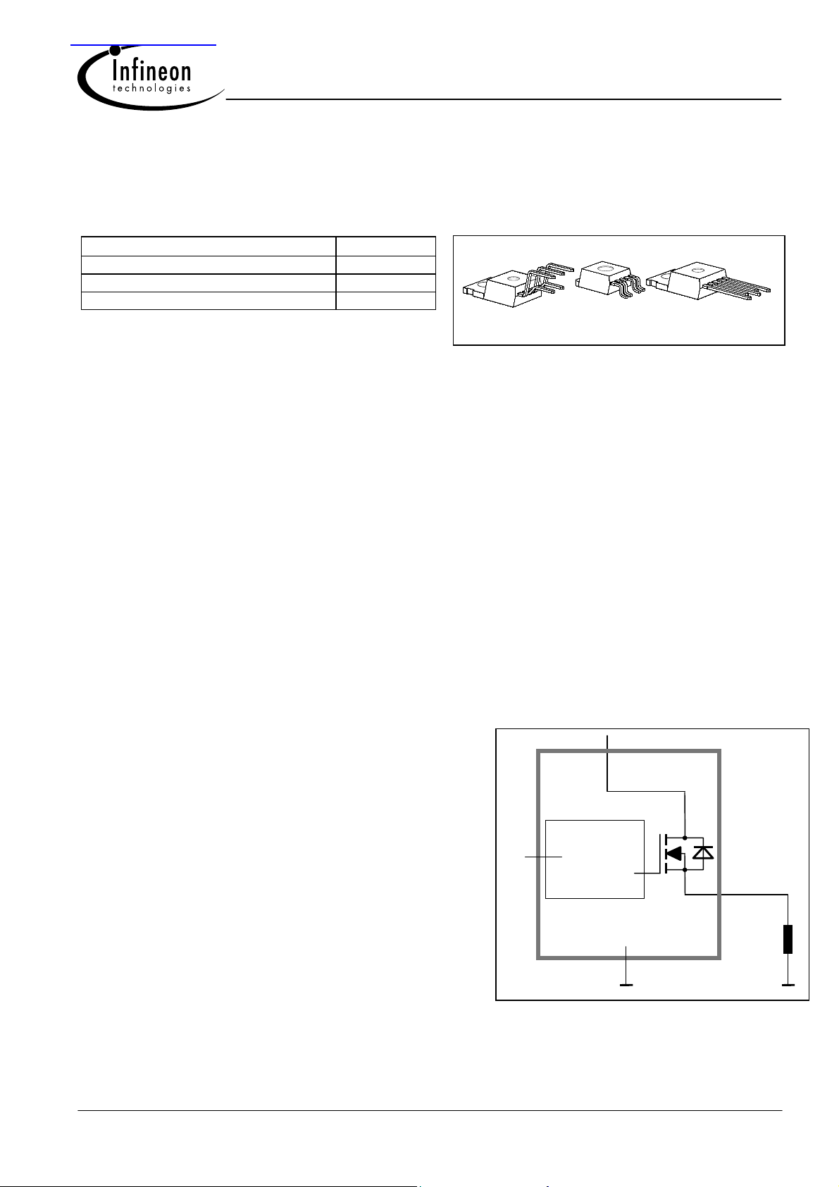
TO-220-5-11 TO-263-5-2 TO-220-5-12
Standard SMD Straight
Application
• µC compatible power switch for 5V, 12 V and 24 V DC applications
• All types of resistive, inductive and capacitve loads
• Most suitable for loads with high inrush currents, so as lamps
• Replaces electromechanical relays, fuses and discrete circuits
Basic Funktions
• Very low standby current
• Optimized static electromagnetic compatibility (EMC)
• µC and CMOS compatible
• Fast demagnetization of inductive loads
• Stable behaviour at undervoltage
Protection Functions
• Short circuit protection
• Current limitation
• Overload protection
• Thermal shutdown
• Overvoltage protection (including load dump) with external
GND-resistor
• Reverse battery protection with external GND-resistor
• Loss of ground and loss of Vbb protection
• Electrostatic discharge (ESD) protection
IN
Vbb
Logic
with
protection
functions
PROFET
OUT
Load
GND
Infineon Technologies AG 1 of 11 2003-Oct-01
BTS 441 T
p
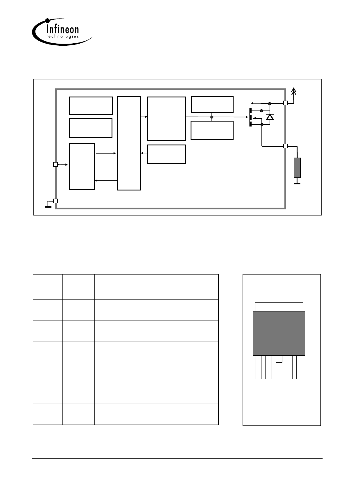
Functional diagram
IN
overvoltage
rotection
internal
voltage supply
ESD
logic
gate
control
+
charge
pump
temperature
sensor
current limit
clamp for
inductive load
VBB
OUT
LOAD
GND
PROFET
Pin Definitions and Functions
Pin
Symbol Function
1
2 IN
3 Vbb
GND
Input, activates the power switch in
case of logical high signal
Positive power supply voltage
The tab is shorted to pin 3
4 N.C.
5 OUT
Tab Vbb
Positive power supply voltage
The tab is shorted to pin 3
Logic ground
Not connected
Output to the load
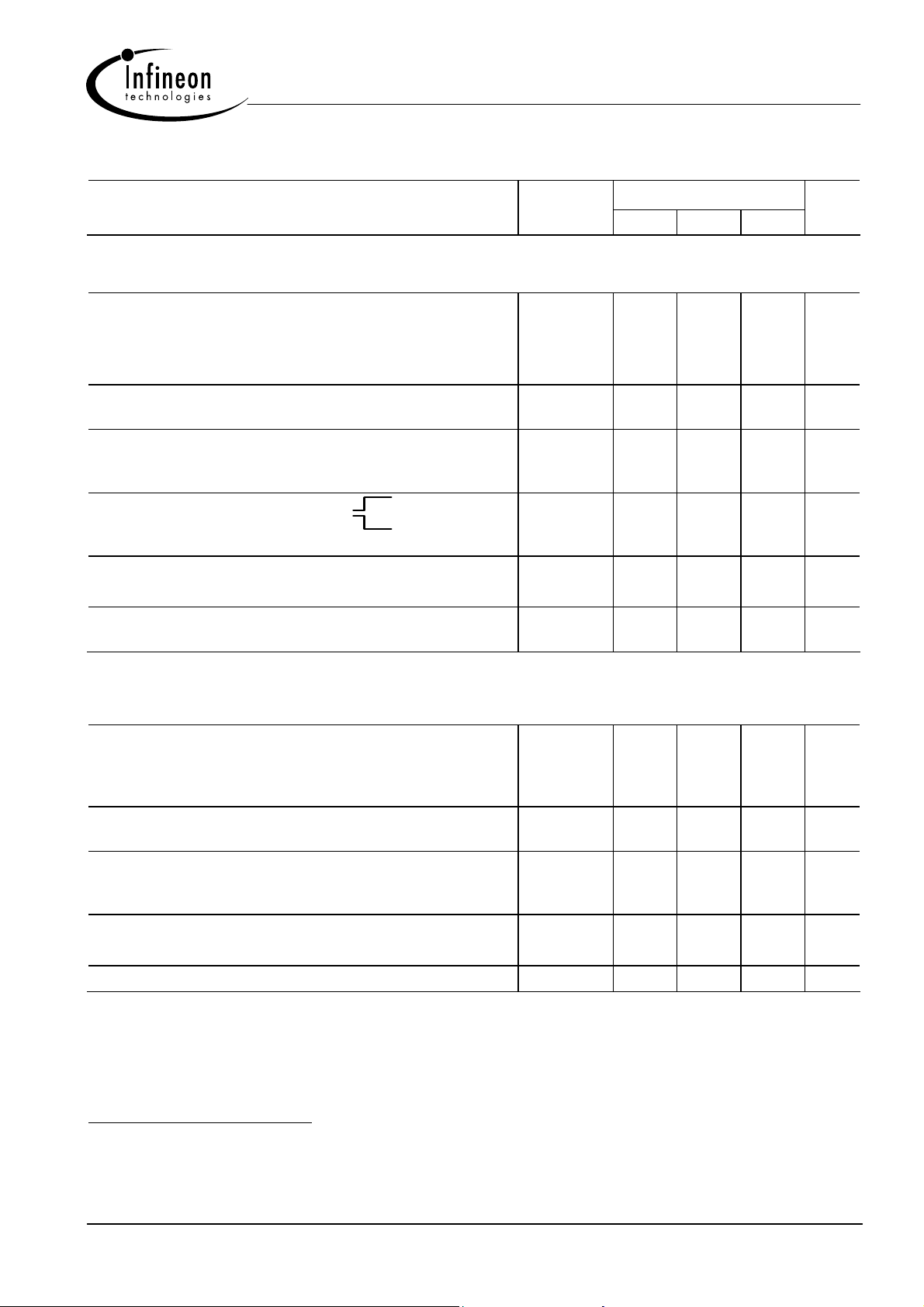
Pin configuration
(top view)
Tab = V
BB
1 2 (3) 4 5
GND IN NC OUT
Infineon Technologies AG 2 2003-Oct-01

BTS 441 T
Maximum Ratings at Tj = 25 °C unless otherwise specified
Parameter Symbol Values Unit
Supply voltage (overvoltage protection see page 4) Vbb 43 V
Supply voltage for full short circuit protection
T
=-40 ...+150°C
j Start
Load dump protection1) V
2)
R
= 2 Ω, RL= 0,5 Ω, td= 200 ms, IN= low or high
I
LoadDump
= VA + Vs, VA = 13.5 V
Load current (Short-circuit current, see page 5) IL self-limited A
Operating temperature range
Storage temperature range
Power dissipation (DC) ; TC≤25°C P
Maximal switchable inductance, single pulse
V
= 12V, T
bb
(see diagram, p.8) I
= 150°C, TC = 150°C const.
j,start
= 21 A, RL= 0 Ω: E
L(ISO)
4)
AS
=0.7J:
Electrostatic discharge capability (ESD) IN:
(Human Body Model) Out to all other pins shorted:
acc. MIL-STD883D, method 3015.7 and
ESD assn. std. S5.1-1993; R=1.5kΩ; C=100pF
Input voltage (DC) VIN -10 ... +16 V
Current through input pin (DC)
see internal circuit diagrams page 7
Thermal resistance chip - case:
junction - ambient (free air):
SMD version, device on pcb5): ≤ 33
Vbb 34 V
V
Load dump
T
j
T
stg
125 W
tot
3)
60 V
-40 ...+150
-55 ...+150
°C
ZL 2.1 mH
V
1.0
ESD
kV
8.0
I
IN
±2.0 mA
R
R
thJC
thJA
≤ 1
≤ 75
K/W
1)
Supply voltages higher than V
resistor in the GND connection. A resistor for the protection of the input is integrated.
2)
RI = internal resistance of the load dump test pulse generator
3)
V
Load dump
4)
E
AS
5)
Device on 50mm*50mm*1.5mm epoxy PCB FR4 with 6cm2 (one layer, 70µm thick) copper area for Vbb
connection. PCB is vertical without blown air.
is setup without the DUT connected to the generator per ISO 7637-1 and DIN 40839
is the maximum inductive switch off energy
require an external current limit for the GND pin, e.g. with a 150 Ω
bb(AZ)
Infineon Technologies AG 3 2003-Oct-01
BTS 441 T
Electrical Characteristics
Parameter and Conditions Symbol Values Unit
at Tj =-40...+150°C, Vbb = 12 V unless otherwise specified
Load Switching Capabilities and Characteristics
min typ max
On-state resistance (V
IL = 2 A Vbb≥7V
T
see diagram page 9
Tj=25 °C:
:
Nominal load current (pin 3 to 5)
‘ISO 10483-1, 6.7:V
=0.5V, TC=85°C
ON
Output current (pin 5) while GND disconnected or
6)
GND pulled up
see diagram page 7
, Vbb=30 V, VIN= 0,
Turn-on time IN
Turn-off time IN
(pin3) to OUT (pin5));
bb
to 90% V
to 10% V
=150 °C:
j
OUT
OUT
:
:
RON
I
I
t
t
L(ISO)
L(GNDhigh)
on
off
RL = 12 Ω,
Slew rate on
10 to 30% V
Slew rate off
70 to 40% V
, R
OUT
OUT
= 12 Ω,
L
, RL = 12 Ω,
dV /dton 0.1 -- 1 V/µs
-dV/dt
Operating Parameters
Operating voltage Tj =-40°C
V
Tj =+25°C
Tj =+105°C
6)
Tj =+150°C
Overvoltage protection
I
= 40 mA Tj =+25...+150°C:
bb
Standby current (pin 3)
VIN=0 see diagram page 9 T
Off-State output current (included in I
VIN=0
Operating current (Pin 1)9), VIN=5 V,
7)
Tj =-40°C:
8)
Tj=-40...+25°C:
Tj=+105°C6):
=+150°C:
j
)
bb(off)
V
I
bb(off)
I
L(off)
I
GND
--
15
28
20
37
17 21 -- A
-- -- 2 mA
40
0.1 -- 1 V/µs
off
4.75
bb(on)
40
4.75
4.75
5.0
bb(AZ)
41
43
--
--
--
90
110
--
--
--
--
--
47
5
--
--
200
250
41
43
43
43
-52
10
10
25
-- 1.5 10 µA
-- 2 4 mA
mΩ
µs
V
V
µA
6)
not subject to production test, specified by design
7)
see also V
8)
Measured with load, typ. 40 µA without load.
9)
Add IIN, if VIN>5.5 V
in table of protection functions and circuit diagram page 7
ON(CL)
Infineon Technologies AG 4 2003-Oct-01
 Loading...