

INFINEON BTS 4141N User Manual
Smart High-Side Power Switch
)
)
1 Channel: 1 x 200mΩ
BTS 4141N
Features
• Short circuit protection
• Current limitation
• Overload protection
Product Summary
Overvoltage protection V
Operating voltage V
On-state resistance R
• Overvoltage protection (including load dump)
• Undervoltage shutdown with auto-
restart and hysteresis
• Switching inductive loads
• Clamp of negative voltage at output
with inductive loads
• CMOS compatible input
• Thermal shutdown with restart
• ESD - Protection
• Loss of GND and loss of V
protection
bb
• Very low standby current
bb(AZ
bb(on
ON
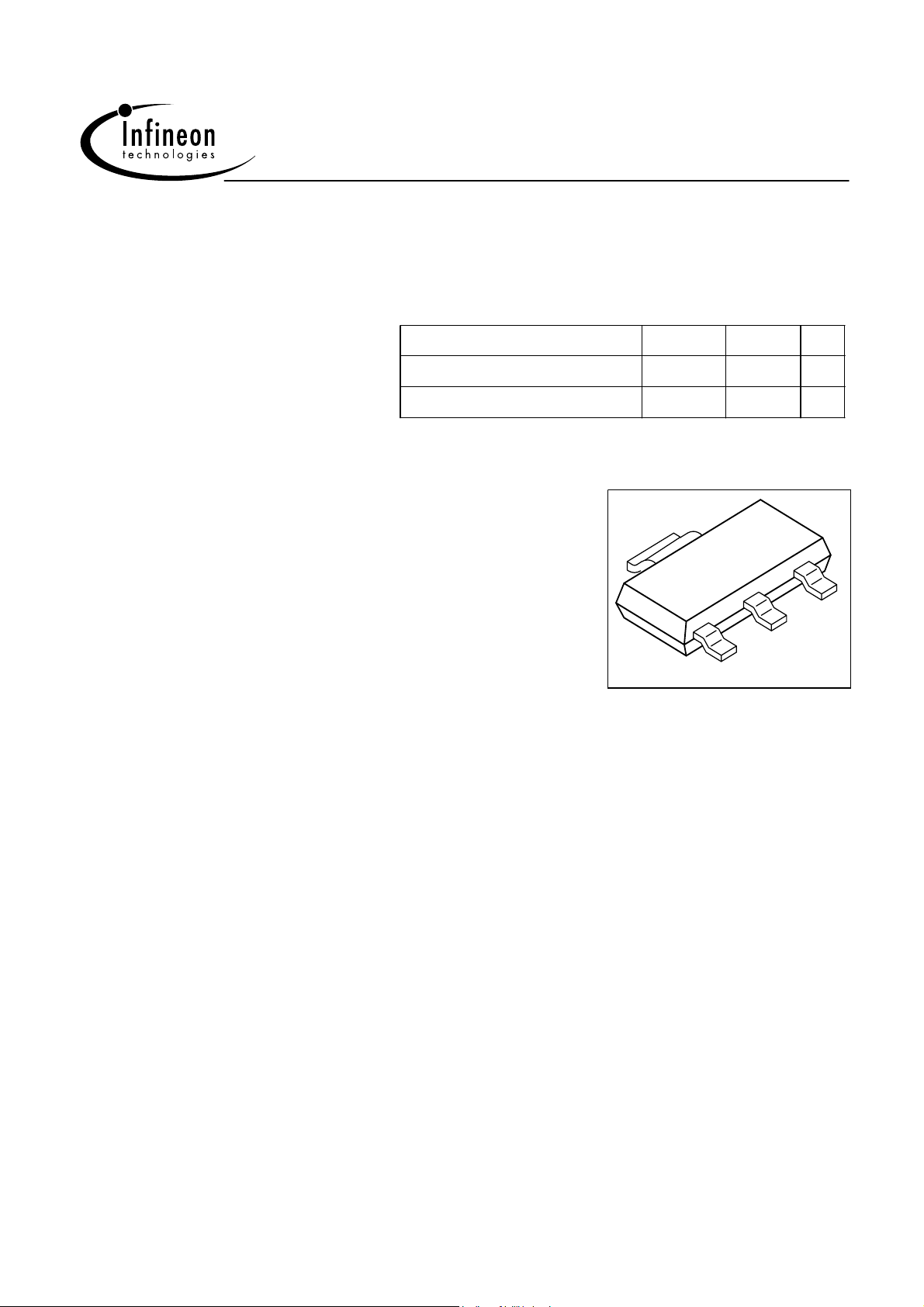
SOT-223
4
47 V
12...45 V
200 mΩ
2
1
VPS05163
3
• Reverse battery protection with external resistor
• Improved electromagnetic compatibility (EMC)
Application
• All types of resistive, inductive and capacitive loads
• µC compatible power switch for 12 V and 24 V DC applications
• Replaces electromechanical relays and discrete circuits
General Description
N channel vertical power FET with charge pump, ground referenced CMOS compatible input,
monolithically integrated in Smart SIPMOS technology.
Providing embedded protective functions.
Page 1
2004-01-27
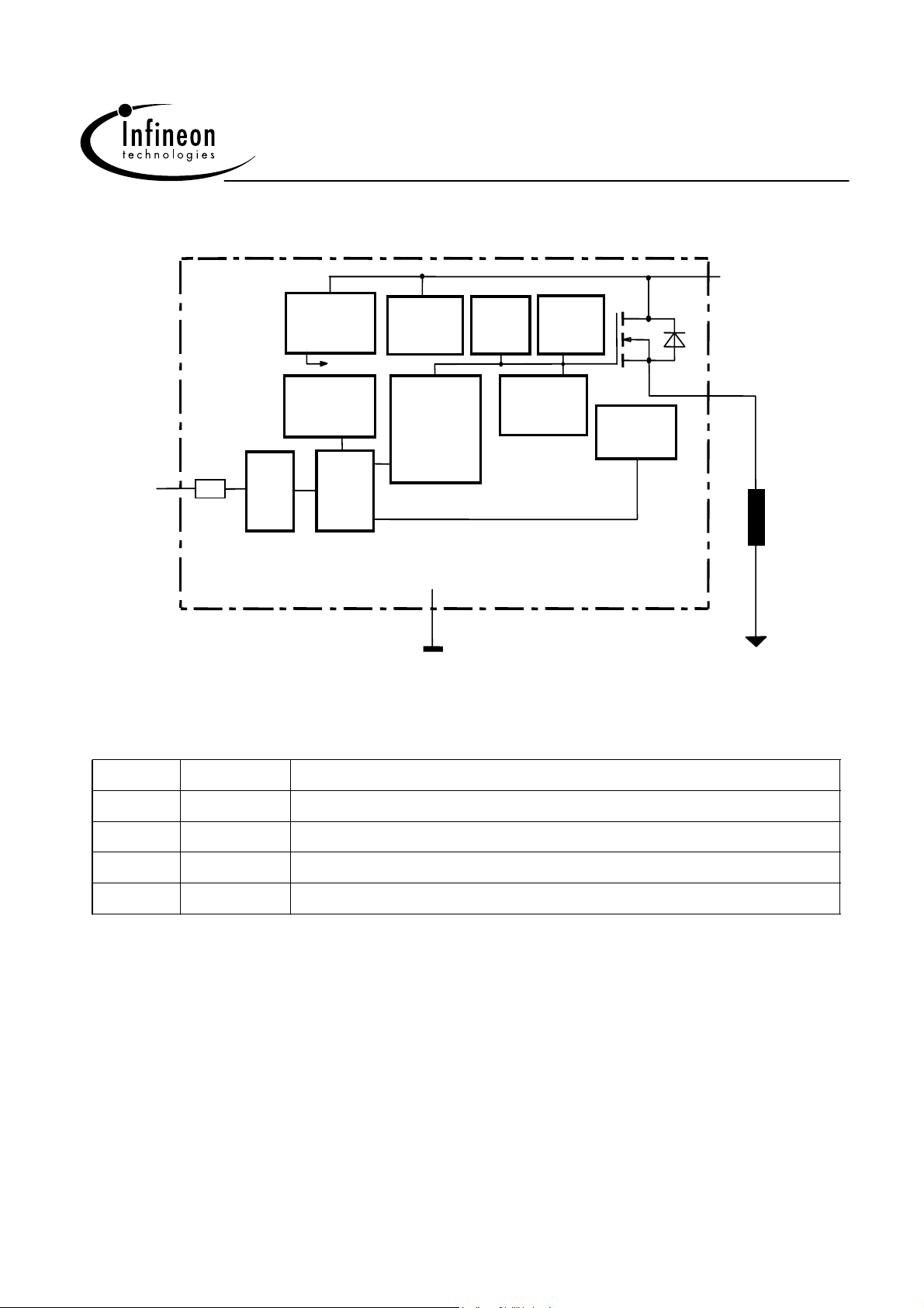
Block Diagram
R
in
3
IN
ESD
Volt age
source
V
Logic
Voltage
sensor
Logic
Overvol tage
protection
Charge pump
Level shifter
Rectifier
Curr ent
limit
Gat e
protection
Limit for
unclamped
ind. loads
Temperature
sensor
+ V
bb
OUT
BTS 4141N
4
1
Load
Pin Symbol
1
2
3
4
OUT
GND
IN
Vbb
GND
miniPROFET
®
2
Signal GND
Load GND
Function
Output to the load
Logic ground
Input, activates the power switch in case of logic high signal
Positive power supply voltage
Page 2
2004-01-27

Maximum Ratings
BTS 4141N
Parameter
Symbol Value Unit
at Tj = 25°C, unless otherwise specified
Supply voltage V
Continuous input voltage
2)
V
Load current (Short - circuit current, see page 5) I
Current through input pin (DC) I
Reverse current through GND-pin
3)
-I
Operating temperature T
Storage temperature T
Power dissipation
4)
Inductive load switch-off energy dissipation
4)5)
P
E
single pulse
T
= 125 °C, IL = 0.5 A
j
Load dump protection5) V
R
=2Ω, t
I
R
= 47 Ω
L
=400ms, VIN= low or high, VA=13,5V
d
LoadDump
6)
= VA + V
V
S
bb
IN
L
IN
GND
j
stg
tot
AS
Loaddump
-0,31)...48
-10...V
bb
V
self limited A
±5
mA
-0.5 A
internal limited °C
-55 ... +150
1.4 W
0.7 J
V
83
Electrostatic discharge voltage (Human Body Model)
V
ESD
according to ANSI EOS/ESD - S5.1 - 1993
ESD STM5.1 - 1998
Input pin
All other pins
1
defined by P
2
At VIN > Vbb, the input current is not allowed to exceed ±5 mA.
3
defined by P
4
Device on 50mm*50mm*1.5mm epoxy PCB FR4 with 6 cm2 (one layer, 70µm thick) copper area for Vbb
connection. PCB is vertical without blown air.
5
not subject to production test, specified by design
6
V
Loaddump
Supply voltages higher than V
150Ω resistor in GND connection. A resistor for the protection of the input is integrated.
tot
tot
is setup without the DUT connected to the generator per ISO 7637-1 and DIN 40839 .
require an external current limit for the GND pin, e.g. with a
bb(AZ)
±1
±5
kV
Page 3
2004-01-27

BTS 4141N
)
)
Electrical Characteristics
Parameter Symbol Values Unit
at Tj = -40...125 °C, Vbb = 15...30 V unless otherwise specified min. typ. max.
Thermal Characteristics
Thermal resistance @ min. footprint R
Thermal resistance @ 6 cm2 cooling area
1)
Thermal resistance, junction - soldering point R
Load Switching Capabilities and Characteristics
On-state resistance
T
= 25 °C, IL = 0.5 A
j
T
= 125 °C
j
1)
2)
OUT
OUT
OUT
,
Nominal load current
Device on PCB
Turn-on time to 90% V
R
= 47 Ω, V
L
= 0 to 10 V
IN
Turn-off time to 10% V
R
= 47 Ω, V
L
= 10 to 0 V
IN
Slew rate on 10 to 30% V
R
= 47 Ω, V
L
= 15 V
bb
th(JA
R
th(JA
thJS
R
ON
I
L(nom)
t
on
t
off
dV/dt
on
- - 125 K/W
- - 70
- - 7 K/W
-
-
150
270
200
320
mΩ
0.7 - - A
µs
- 50 100
- 75 150
V/µs
- 1 2
Slew rate off 70 to 40% V
R
= 47 Ω, V
L
1
Device on 50mm*50mm*1.5mm epoxy PCB FR4 with 6 cm2 (one layer, 70µm thick) copper area for Vbb
connection. PCB is vertical without blown air.
2
Nominal load current is limited by the current limitation ( see page 5 )
= 15 V
bb
OUT
,
-dV/dt
off
- 1 2
Page 4
2004-01-27

BTS 4141N
)
)
)
j
j
Electrical Characteristics
Parameter Symbol Values Unit
at Tj = -40...125 °C, Vbb = 15...30 V unless otherwise specified min. typ. max.
Operating Parameters
Operating voltage V
Undervoltage shutdown V
Undervoltage restart V
Undervoltage hysteresis
∆V
bb(under)
= V
bb(u rst)
- V
bb(under)
Standby current
T
= -40...85 °C, V
j
Tj = 125 °C
1)
≤ 1,2 V
IN
Operating current I
Leakage output current (included in I
V
≤ 1,2 V
IN
Protection Functions
2)
bb(off)
)
Initial peak short circuit current limit
T
= -40 °C, Vbb = 20 V, tm = 150 µs
j
T
= 25 °C
j
T
= 125 °C
j
bb(on
bb(under
bb(u rst
∆V
bb(under)
I
bb(off)
GND
I
L(off)
I
L(SCp)
12 - 45 V
7 - 10.5
- - 11
- 0.5 -
-
-
10
25
-
50
- 1 1.6 mA
- 3.5 10 µA
-
-
0.7
-
1.4
-
2.1
-
-
µA
A
Repetitive short circuit current limit
I
L(SCr)
- 1.1 -
Tj = Tjt (see timing diagrams)
Output clamp (inductive load switch off)
at V
OUT
= Vbb - V
ON(CL)
, Ibb = 4 mA
Overvoltage protection 3)
V
ON(CL)
V
bb(AZ)
62 68 - V
47 - -
Ibb = 4 mA
Thermal overload trip temperature
Thermal hysteresis ∆T
1
higher current due temperature sensor
2
Integrated protection functions are designed to prevent IC destruction under fault conditions
described in the data sheet. Fault conditions are considered as "outside" normal operating range.
Protection functions are not designed for continuous repetitive operation.
3
see also V
4
higher operating temperature at normal function available
ON(CL)
in circuit diagram
4)
Page 5
T
t
t
135 - - °C
- 10 - K
2004-01-27

BTS 4141N
)
)
)
)
)
Electrical Characteristics
Parameter Symbol Values Unit
at Tj = -40...125 °C, Vbb = 15...30 V unless otherwise specified min. typ. max.
Input
Continuous input voltage
1)
V
Input turn-on threshold voltage V
Input turn-off threshold voltage V
Input threshold hysteresis ∆V
Off state input current
V
≤ 1,8 V
IN
On state input current I
Input delay time at switch on V
bb
I
IN(off)
IN(on
t
d(Vbbon
Input resistance (see page 8) R
IN
IN(T+
IN(T-
IN(T
I
-10
2)
-
V
bb
- - 3.0
1.82 - -
- 0.2 -
20 - -
- - 110
150 340 - µs
1.5 3 5
V
µA
kΩ
Reverse Battery
Reverse battery voltage
R
R
GND
GND
= 0 Ω
= 150 Ω
3)2)
Continuous reverse drain current2)
T
= 25 °C
j
Drain-source diode voltage (V
I
= 1 A
F
OUT
> Vbb)
-V
I
S
-V
bb
ON
-
-
-
-
0.3
45
V
- - 1 A
- 0.6 1.2 V
1
At VIN > Vbb, the input current is not allowed to exceed ±5 mA.
2
not subject to production test, guaranted by design
3
defined by P
tot
Page 6
2004-01-27
 Loading...