

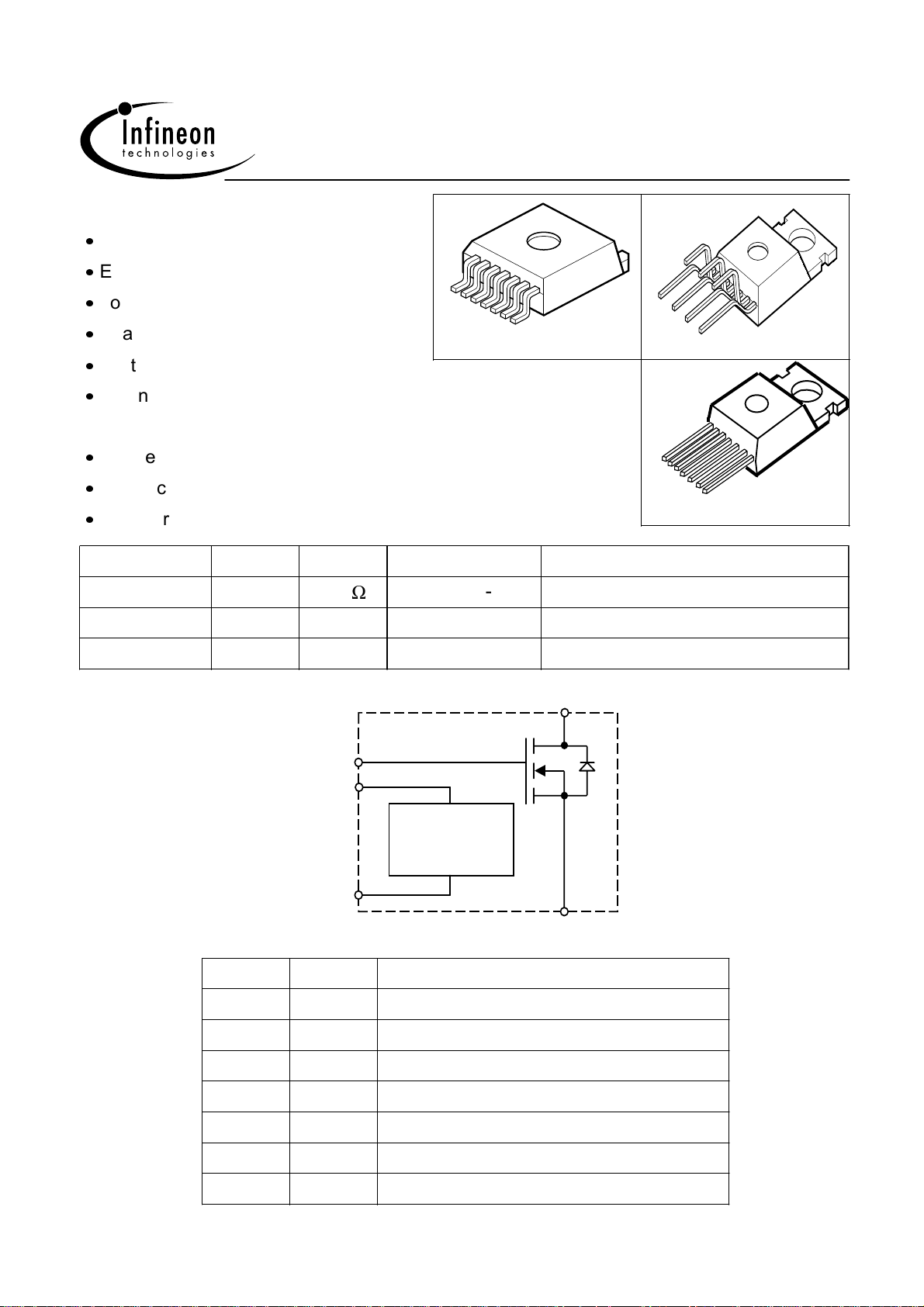
Speed TEMPFET
N-Channel
Enhancement mode
BTS 282 Z
Logic Level Input
Analog driving possible
Fast switching up to 1 MHz
Potential-free temperature sensor with
thyristor characteristics
Overtemperature protection
Avalanche rated
High current pinning
Type
BTS 282 Z 49 V
V
DS
R
DS(on)
6.5 m
1
7
VPT05754
1
1
Package Ordering Code
P-TO220-7-3 Q67060-S6004-A2
P-TO220-7-180 Q67060-S6005-A2
P-TO220-7-230 Q67060-S6007
D Pin 4 and TAB
7
VPT05167
7
G Pin 2
A Pin 3
Temperature
Sensor
K Pin 5
S Pin 1 + 6 + 7
Pin Symbol Function
1 S Source
2 G Gate
3 A Anode Temperature Sensor
4 D Drain
5 K Cathode Temperature Sensor
6 S Source
7 S Source
1
2000-09-11

BTS 282 Z
j
jp
g
Maximum Ratings
Parameter Symbol Value Unit
Drain source voltage
Drain-gate voltage, RGS = 20 k
Gate source voltage
Nominal load current (ISO 10483)
V
= 4.5 V, VDS 0.5 V, TC = 85 °C
GS
VGS = 10 V, VDS 0.5 V, TC = 85 °C
Continuous drain current 1)
TC = 100 °C, VGS = 4.5V
Pulsed drain current
Avalanche energy, single pulse
ID = 36 A, RGS = 25
Power dissipation
TC = 25 °C
Operating temperature
2)
V
DS
V
DGR
V
GS
I
D(ISO)
I
D
I
D puls
E
AS
P
tot
T
49
V
49
20
A
36
52
80
320
2 J
300 W
-40 ...+175 °C
Peak temperature ( single event )
Storage temperature
T
eak
T
st
200
-55 ... +150
DIN humidity category, DIN 40 040 E
IEC climatic category; DIN IEC 68-1 40/150/56
1
current limited by bond wire
2
Note: Thermal trip temperature of temperature sensor is below 175°C
2
2000-09-11

BTS 282 Z
)
)
Thermal Characteristics
Parameter Symbol Values Unit
min. typ. max.
Characteristics
junction - case:
Thermal resistance @ min. footprint
Thermal resistance @ 6 cm2 cooling area
Electrical Characteristics
Parameter
at Tj = 25°C, unless otherwise specified
Static Characteristics
Drain-source breakdown voltage
V
= 0 V, ID = 0.25 mA
GS
Gate threshold voltage, VGS = VDS
I
= 240 µA
D
Zero gate voltage drain current
V
= 45 V, VGS = 0 V, Tj = -40 °C
DS
V
= 45 V, VGS = 0 V, Tj = 25 °C
DS
V
= 45 V, VGS = 0 V, Tj = 150 °C
DS
1)
R
R
R
thJC
th(JA
th(JA
- - 0.5 K/W
- - 62
- 33 40
Symbol Values Unit
min. typ. max.
V
(BR)DSS
V
GS(th)
I
DSS
49 - - V
1.2 1.6 2
-
-
-
-
0.1
-
0.1
1
100
µA
Gate-source leakage current
V
= 20 V, VDS = 0 V, Tj = 25 °C
GS
V
= 20 V, VDS = 0 V, Tj = 150 °C
GS
Drain-Source on-state resistance
V
= 4.5 V, ID = 36 A
GS
V
= 10 V, ID = 36 A
GS
1
Device on 50mm*50mm*1.5mm epoxy PCB FR4 with 6cm
connection. PCB mounted vertical without blown air.
I
GSS
-
-
R
DS(on)
-
-
2 (one layer, 70µm thick) copper area for drain
3
10
20
8.2
5.8
100
100
9.5
6.5
nA
m
2000-09-11

Electrical Characteristics
BTS 282 Z
Parameter
at Tj = 25°C, unless otherwise specified
Dynamic Characteristics
Forward transconductance
V
>2*ID*R
DS
DS(on)max
, ID = 80 A
Input capacitance
V
= 0 V, VDS = 25 V, f = 1 MHz
GS
Output capacitance
V
= 0 V, VDS = 25 V, f = 1 MHz
GS
Reverse transfer capacitance
V
= 0 V, VDS = 25 V, f = 1 MHz
GS
Turn-on delay time
V
= 30 V, VGS = 4.5 V, ID = 80 A,
DD
R
= 1.3
G
Rise time
V
= 30 V, VGS = 4.5 V, ID = 80 A,
DD
R
= 1.3
G
Symbol Values Unit
min. typ. max.
g
fs
C
iss
C
oss
C
rss
t
d(on)
t
r
30 70 - S
- 3850 4800 pF
- 1090 1357
- 570 715
- 30 45 ns
- 37 56
Turn-off delay time
V
= 30 V, VGS = 4.5 V, ID = 80 A,
DD
R
= 1.3
G
Fall time
V
= 30 V, VGS = 4.5 V, ID = 80 A,
DD
R
= 1.3
G
Gate Charge Characteristics
Gate charge at threshold
V
= 40 V, ID=≥0,1 A , VGS = 0 to 1 V
DD
Gate charge at 5.0 V
V
= 40 V, ID = 80 A, VGS = 0 to 5 V
DD
Gate charge total
V
= 40 V, ID = 80 A, VGS = 0 to 10 V
DD
Gate plateau voltage
V
= 40 V, ID = 80 A
DD
t
d(off)
t
f
Q
g(th)
Q
g(5)
Q
g(total)
V
(plateau)
- 70 105
- 36 55
- 3.8 5.7 nC
- 92 138
- 155 232
- 3.4 - V
4
2000-09-11

Electrical Characteristics
BTS 282 Z
Parameter
at Tj = 25°C, unless otherwise specified
Symbol Values Unit
min. typ. max.
Reverse Diode
Inverse diode continuous forward current
= 25 °C
T
C
Inverse diode direct current,pulsed
= 25 °C
T
C
Inverse diode forward voltage
= 0 V, IF = 95 A
V
GS
Reverse recovery time
= 30 V, IF=IS, diF/dt = 100 A/µs
V
R
Reverse recovery charge
= 30 V, IF=IS, diF/dt = 100 A/µs
V
R
I
I
V
t
Q
S
FM
SD
rr
rr
80 - - A
320 - -
- 1.25 1.6 V
- 105 157 ns
- 0.31 0.47 µC
Sensor Characteristics
For temperature sensing, i.e. temperature protection, please consider application note
"Temperature sense concept - Speed TEMPFET”.
For short circuit protection please consider application note "Short circuit behaviour of
the Speed TEMPFET family”.
All application notes are available at http://www.infineon.com/tempfet/
Forward voltage
I
AK(on)
I
AK(on)
= 5 mA, Tj = -40...+150 °C
= 1.5 mA, Tj = 150 °C
Sensor override
t
= 100 µs, Tj = -40...+150 °C
P
Forward current
T
= -40...+150 °C
j
Sensor override
t
= 100 µs, Tj = -40...+150 °C
P
V
AK(on)
I
AK(on)
-
-
1.3
-
1.4
0.9
- - 10
- - 5 mA
- - 600
V
5
2000-09-11

Electrical Characteristics
(
)
BTS 282 Z
Parameter
at Tj = 25°C, unless otherwise specified
Sensor Characteristics
Temperature sensor leakage current
= 150 °C
T
j
Min. reset pulse duration 1)
= -40...+150 °C, I
T
j
V
AK
Reset
<0.5V
VAK Recovery time
= -40...+150 °C, I
T
j
AK(on)
1)2)
AK(on)
= 0.3 mA,
= 0.3 mA
Characteristics
Holding current, V
= 25 °C
T
j
T
= 150 °C
j
AK(off)
= 5V
Symbol Values Unit
min. typ. max.
I
AK(off)
t
reset
t
recovery
I
AK(hold)
- - 4 µA
100 - - µs
- - 150
0.05
0.05
-
-
0.5
0.3
mA
Thermal trip temperature
V
= 5V
TS
Turn-off time (Pin G+A and K+S connected)
V
= 5V, I
TS
TS(on)
= 2 mA
Reset voltage
T
= -40...+150°C
j
Sensor recovery behaviour:
Sensor RESET
t
V
[V ]
AK
5
4
0
res et
t
recovery
ON Reset OFFSensor
T
TS(on)
t
off
V
AK(reset)
150 160 170 °C
0.5 - 2.5 µs
0.5 - - V
1
See diagram Sensor recovery behaviour
2
Time after reset pulse until VAK reaches 4V again
6
2000-09-11
BTS 282 Z
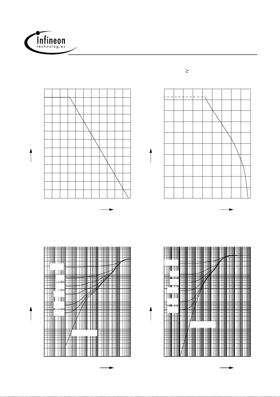
1 Maximum allowable power dissipation
= f(TC)
P
tot
325
W
275
250
225
tot
200
P
175
150
125
100
75
50
25
0
-40 0 40 80 120
°C
180
T
C
2 Drain current
I
= f(TC); VGS 4.5V
D
100
A
80
70
D
I
60
50
40
30
20
10
0
0 20 40 60 80 100 120 140
°C
180
T
C
3 Typ. transient thermal impedance
Z
=f(tp) @ 6 cm2 cooling area
thJA
Parameter: D=t
2
10
K/W
D=0.5
1
10
thJA
Z
0
10
-1
10
-2
10
-5
10
10
0.2
0.1
0.05
0.02
0.01
-4
p
10
/T
-3
Single pulse
-2
10
10
-1
10 0 10
1
4 Transient thermal impedance
= f (tp)
Z
thJC
parameter : D = t
0
10
K/W
D=0.5
-1
-2
-3
-4
10
0.05
0.02
0.01
-8
0.2
0.1
10
-7
10
thJC
Z
10
10
3
s
10
t
p
10
10
p
-6
-5
10
/T
Single pulse
-4
-3
10
10
10
-2
10
-1
10 0 10
1
3
s
10
tp
7
2000-09-11

BTS 282 Z
5 Safe operating area
I
=f(VDS); D=0.01; TC=25°C; VGS=4.5V
D
3
10
A
2
10
D
I
1
10
0
10
10
0
10
1
V
30µsRdson=Vds/Id
100µs
1ms
10ms
100ms
DC
V
DS
10
6 Typ. output characteristic
= f(VDS); Tj=25°C
I
D
Parameter: V
2
200
A
160
140
D
I
120
100
80
60
40
20
0
0 1 2
GS
10V
6V
7V
5V
4.5V
4V
3.5V
3V
V
4
V
DS
7 On-state resistance
R
= f(Tj); ID=36A; V
ON
20
m
16
14
DS(on)
R
12
10
8
6
4
2
GS
= 4.5V
max.
typ.
8 On-state resistance
R
= f(Tj); ID=36A; VGS = 10V
ON
14
m
10
DS(on)
R
8
6
4
2
max.
typ.
0
-50 -25 0 25 50 75 100 125
°C
175
T
j
0
-50 -25 0 25 50 75 100 125
8
°C
175
T
j
2000-09-11

BTS 282 Z
j
9 Typ. transfer characteristics
I
= f(VGS); VDS = 12V; Tj = 25°C
D
150
A
120
110
100
D
I
90
80
70
60
50
40
30
20
10
0
0.0 0.5 1.0 1.5 2.0 2.5 3.0 3.5 4.0
10 Typ. input threshold voltage
V
GS(th)
= f(Tj); VDS=V
GS
Parameter: ID
2.4
V
2.0
1.8
°C
T
240mA
24mA
2.4mA
240µA
175
j
1.6
GS(th)
V
1.4
1.2
1.0
0.8
0.6
0.4
0.2
V
5.0
V
GS
0.0
-50 -25 0 25 50 75 100 125
11 Typ. capacitances
C = f(V
C
10
); VGS=0 V, f=1 MHz
DS
2
10
nF
1
10
0
10
-1
0 5 10 15 20 25 30
Ciss
V
V
Coss
Crss
DS
40
12 Typ. reverse diode forward
I
charcteristics
t
= 80µs (spread); Parameter: T
p
3
10
A
2
10
F
I
1
10
0
10
-1
10
0.0 0.2 0.4 0.6 0.8 1.0
= f(VSD)
F
150°C
25°C
V
1.4
V
SD
9
2000-09-11
BTS 282 Z
13 Typ. gate charge
V
= f(Q
GS
Parameter: I
BTS 282 Z
16
V
12
GS
10
V
8
6
4
2
0
0 40 80 120 160
Gate
D puls
)
= 80 A
0,2
V
DS max
0,8 V
DS max
nC
Q
240
Gate
14 Drain-source break down voltage
V
(BR)DSS
(BR)DSS
V
= f(Tj)
58
V
56
55
54
53
52
51
50
49
48
47
46
45
-50 -25 0 25 50 75 100 125
°C
Tj
175
10
2000-09-11

BTS 282 Z
Package Ordering Code
P-TO220-7-3 Q67060-S6004-A2
9.9
9.5
3.7
2.8
15.6
0.6
1.27
6 x 7.62
1.27
1) shear and punch direction no burrs this surface
12.8
8.6
10.2
=
1)
4.4
1.3
9.2
3.3
2.4
3.9
8.4
0.5
GPT05167
Package Ordering Code
P-TO220-7-180 Q67060-S6005-A2
9.9
8
A
B
1.3
7.5
6.6
0.05
±0.15
10.5
6.5
(1.3)
1)
0 ... 0.15
+0.1
0.6
-0.03
1.27
6 x 1.27 = 7.62
0.25 M
0.5
AB
1) Shear and punch direction no burrs this surface
Back side, heatsink contour
All metal surfaces tin plated, except area of cut
+0.1
-0.02
0.1
2.4
3.6
+0.15
4.4
5
+3
0.1 B
±0.2
9.2
±0.4
1.5
(14.1)
Package Ordering Code
P-TO220-7-230 Q67060-S6007
11
2000-09-11

BTS 282 Z
Published by
Infineon Technologies AG,
Bereichs Kommunikation
St.-Martin-Strasse 53,
D-81541 München
© Infineon Technologies AG 1999
All Rights Reserved.
Attention please!
The information herein is given to describe certain components and shall not be considered as warranted
characteristics.
Terms of delivery and rights to technical change reserved.
We hereby disclaim any and all warranties, including but not limited to warranties of non-infringement,
regarding circuits, descriptions and charts stated herein.
Infineon Technologies is an approved CECC manufacturer.
Information
For further information on technology, delivery terms and conditions and prices please contact your nearest
Infineon Technologies Office in Germany or our Infineon Technologies Reprensatives worldwide (see address list).
Warnings
Due to technical requirements components may contain dangerous substances.
For information on the types in question please contact your nearest Infineon Technologies Office.
Infineon Technologies Components may only be used in life-support devices or systems with the express
written approval of Infineon Technologies, if a failure of such components can reasonably be expected to
cause the failure of that life-support device or system, or to affect the safety or effectiveness of that device
or system Life support devices or systems are intended to be implanted in the human body, or to support
and/or maintain and sustain and/or protect human life. If they fail, it is reasonable to assume that the health
of the user or other persons may be endangered.
12
2000-09-11
 Loading...