

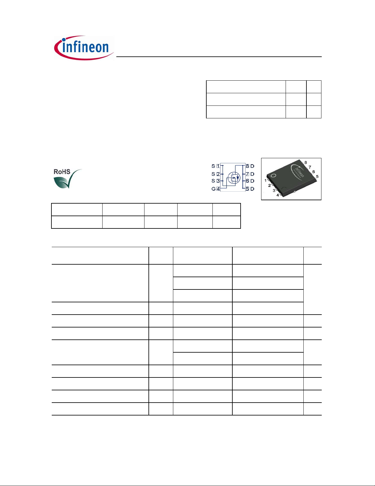
BSC080P03LS G
OptiMOS®-P Power-Transistor
Features
• P-Channel
• Enhancement mode
• Logic level
• 150°C operating temperature
• Avalanche rated
• Vgs=25V, specially suited for notebook applications
Type Package
BSC080P03LS G PG-TDSON-8
Maximum ratings, at T
=25 °C, unless otherwise specified
j
Marking Lead free Packing
080P03LS Yes Dry
Product Summary
V
DS
R
DS(on),max
I
D
-30 V
8
-30 A
PG-TDSON-8
mΩ
Parameter Symbol Conditions Unit
Continuous drain current
Pulsed drain current
Avalanche energy, single pulse
Gate source voltage
Power dissipation
Operating and storage temperature
I
D
I
D,pulse
E
AS
V
GS
P
tot
T
j
, T
TC=25 °C
T
=70 °C
C
=25 °C
T
A
TC=25 °C
ID=-30 A, RGS=25 Ω
TC=25 °C
T
=25 °C
A
stg
1)
2)
1)
ESD class JESD22-C101-HBM
Soldering temperature
IEC climatic category; DIN IEC 68-1
Value
-30
-30
-16
-120
248
±25
89
2.8
-55 ... 150
1C (1kV-2kV)
260 °C
55/150/56
A
mJ
V
W
°C
Rev. 1.1 page 1 2008-07-10

BSC080P03LS G
Parameter Symbol Conditions Unit
Values
min. typ. max.
Thermal characteristics
Thermal resistance,
junction - case
Thermal resistance,
junction - ambient
Electrical characteristics, at T
R
thJC
R
thJA
=25 °C, unless otherwise specified
j
6 cm2 cooling area
- - 1.4 K/W
1)
--50
Static characteristics
Drain-source breakdown voltage
Gate threshold voltage
Zero gate voltage drain current
V
(BR)DSS
V
GS(th)
I
DSS
VGS=0 V, ID=-250µA
VDS=VGS, ID=-250 µA
VDS=-30 V, VGS=0 V,
T
=25 °C
j
-30 - - V
-2.2 -1.5 -1
- -0.1 -1 µA
V
=-30 V, VGS=0 V,
DS
T
=125 °C
j
Gate-source leakage current
Drain-source on-state resistance
Gate resistance
Transconductance
1)
Device on 40 mm x 40 mm x 1.5 mm epoxy PCB FR4 with 6 cm2 (one layer, 70 µm thick) copper area for drain
connection. PCB is vertical in still air.
2)
See Figure 3.
I
GSS
R
DS(on)VGS
R
G
g
fs
VGS=-25 V, VDS=0 V
=-10 V, ID=-30 A
|VDS|>2|ID|R
I
=-30 A
D
DS(on)max
- -10 -100
- -10 -100 nA
- 6.1 8.0
-4-
,
30 60 - S
mΩ
Ω
Rev. 1.1 page 2 2008-07-10

BSC080P03LS G
g
Parameter Symbol Conditions Unit
Values
min. typ. max.
Dynamic characteristics
Input capacitance
Output capacitance
Reverse transfer capacitance
Turn-on delay time
Rise time
Turn-off delay time
Fall time
Gate Char
e Characteristics
Gate to source charge
Gate charge at threshold
Gate to drain charge
Switching charge
3)
C
C
C
t
t
t
t
Q
Q
Q
Q
iss
oss
rss
d(on)
r
d(off)
f
gs
g(th)
gd
sw
=0 V, VDS=-15 V,
V
GS
f =1 MHz
VDD=-15 V, VGS=10 V, I
R
V
V
=-30 A,
D
=6 Ω
G
=-24 V, ID=30 A,
DD
=0 to -10 V
GS
- 4620 6140 pF
- 1430 1900
- 1200 1800
- 13.5 20.3 ns
- 87.0 130.5
- 79.0 118.5
- 108.0 162.0
- -12.7 -16.8 nC
- -7.1 -9.5
- -34.3 -51.4
- -39.8 -58.8
Gate charge total
Gate plateau voltage
Output charge
Reverse Diode
Diode continous forward current
Diode pulse current
Diode forward voltage
Reverse recovery time
Reverse recovery charge
Q
V
plateau
Q
I
S
I
S,pulse
V
SD
t
rr
Q
g
oss
rr
VDD=-15 V, VGS=0 V
=25 °C
T
C
VGS=0 V, IF=-30 A,
T
=25 °C
j
VR=15 V, IF=|IS|,
di
/dt =100 A/µs
F
- -92.0 -122.4
- -2.8 - V
- 25.6 34.0
- - 30.0 A
- - -120
- -0.9 -1.2 V
-3544ns
- 28.0 - nC
Rev. 1.1 page 3 2008-07-10

1 Power dissipation 2 Drain current
P
=f(TC); tp≤10 s ID=f(TC); |VGS|≥10 V; tp≤10 s
tot
BSC080P03LS G
100
90
32
28
80
24
70
[W]
tot
P
60
50
40
[A]
D
-I
20
16
12
30
8
20
10
0
0 40 80 120 160
TC [°C]
4
0
0 40 80 120 160
TC [°C]
3 Safe operating area 4 Max. transient thermal impedance
Z
I
=f(VDS); TC=25 °C1); D =0
D
parameter: t
p
1000
=f(tp)
thJS
parameter: D =tp/T
1
10
10
1
100 µs
1 ms
10 ms
DC
1 µs
10
0
1
10
0.5
0.2
[K/W]
thJS
0.1
Z
-1
0.1
0.05
10
0.02
0.01
single pulse
-2
0.01
0.00001 0.0001 0.001 0.01 0.1 1 10
10
2
10
-5
10
-4
10
-3
-2
10
tp [s]
10
-1
10
1
0
10
2
100
10
1
10
10
[A]
D
-I
0
1
10
-1
0.1
10
-2
0.01
0.1 1 10 100
10
-1
10
limited by on-state
resistance
0
10
-VDS [V]
10
Rev. 1.1 page 4 2008-07-10

5 Typ. output characteristics 6 Typ. drain-source on resistance
I
=f(VDS); Tj=25 °C R
D
parameter: V
GS
=f(ID); Tj=25 °C
DS(on)
parameter: V
GS
BSC080P03LS G
70
60
50
-10 V
-4.5 V
-3.5 V
-3.2 V
30
25
-2.5 V
-2.7 V
20
]
40
[A]
D
-I
30
20
10
-3 V
-2.7 V
-2.5 V
-2.3 V
0
0123
-VDS [V]
Ω
[m
15
DS(on)
R
10
5
0
0 10203040
-ID [A]
7 Typ. transfer characteristics 8 Typ. forward transconductance
I
=f(VGS); |VDS|>2|ID|R
D
parameter: T
j
DS(on)max
gfs=f(ID); Tj=25 °C
-3 V
-3.2 V
-3.5 V
-4.5 V
-10 V
60
60
50
40
[A]
30
D
-I
20
10
150 °C
25 °C
0
01234
-VGS [V]
40
[S]
fs
g
20
0
0102030
-ID [A]
Rev. 1.1 page 5 2008-07-10

9 Drain-source on-state resistance 10 Typ. gate threshold voltage
R
=f(Tj); ID=-30 A; VGS=-10 V
DS(on)
=f(Tj); VGS=VDS; ID=-250 µA
V
GS(th)
BSC080P03LS G
12
3
2.5
10
max.
2
]
Ω
[m
DS(on)
R
8
98 %
typ.
[V]
GS(th)
-V
1.5
typ.
1
min.
6
0.5
4
-60 -20 20 60 100 140 180
Tj [°C]
0
-60 -20 20 60 100 140 180
Tj [°C]
11 Typ. capacitances 12 Forward characteristics of reverse diode
C =f(V
); VGS=0 V; f =1 MHz IF=f(VSD)
DS
4
10
parameter: T
100
j
10
C [pF]
Ciss
10
Coss
3
Crss
[A]
F
I
150 °C, typ
25 °C, typ
150 °C, 98%
1
25 °C, 98%
2
10
0 5 10 15 20 25 30
-VDS [V]
0.1
0 0.5 1 1.5
-VSD [V]
Rev. 1.1 page 6 2008-07-10

13 Avalanche characteristics 14 Typ. gate charge
V
IAS=f(tAV); RGS=25 Ω
parameter: T
2
10
j(start)
=f(Q
GS
parameter: V
); ID=-30 A pulsed
gate
DD
8
BSC080P03LS G
7
25 °C
-6 V
6
10
1
[A]
AV
-I
100 °C
125 °C
[V]
GS
-V
5
4
3
2
1
0
10
0
0
10
10
1
tAV [µs]
10
2
10
3
0 20406080100
-Q
15 Drain-source breakdown voltage 16 Gate charge waveforms
V
=f(Tj); ID=-250 µA
BR(DSS)
gate
-15 V
-24 V
[nC]
36
V
GS
Q
g
34
32
[V]
BR(DSS)
-V
30
28
26
-60 -20 20 60 100 140 180
V
gs(th)
Q
g(th)
Q
gs
Q
sw
Q
gd
Q
gate
Tj [°C]
Rev. 1.1 page 7 2008-07-10

Package Outline
PG-TDSON-8: Outline
BSC080P03LS G
Dimensions in mm
Rev. 1.1 page 8 2008-07-10

BSC080P03LS G
Rev. 1.1 page 9 2008-07-10

 Loading...