

BSC022N03S
OptiMOS®2 Power-Transistor
Product Summary
Features
• Fast switching MOSFET for SMPS
• Optimized technology for notebook DC/DC converters
1
• Qualified according to JEDEC
for target applications
• N-channel
• Logic level
• Excellent gate charge x R
• Very low on-resistance R
product (FOM)
DS(on)
DS(on)
• Superior thermal resistance
• Avalanche rated
• dv /dt rated
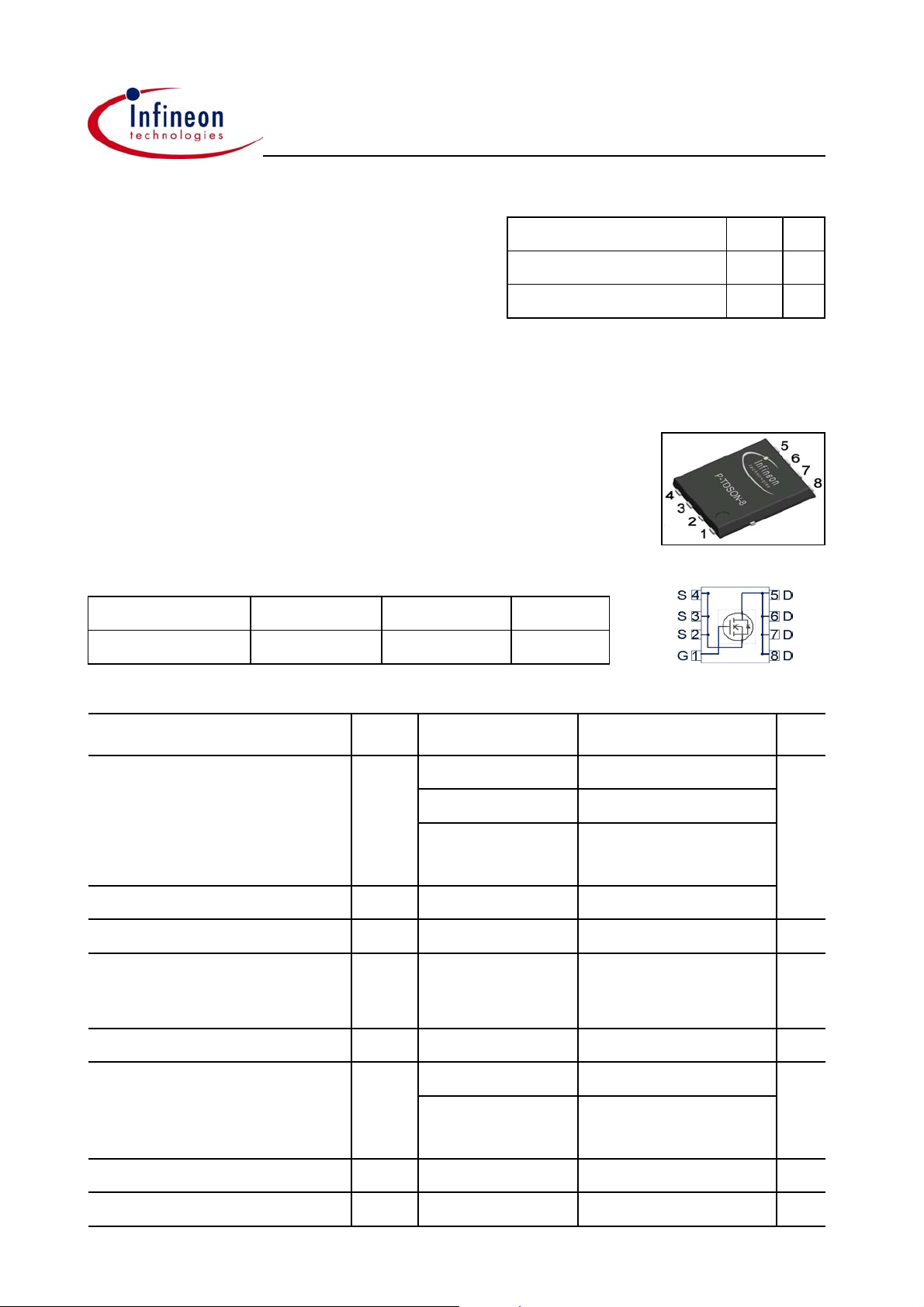
Type Package Ordering Code Marking
V
DS
R
DS(on),max
I
D
30 V
2.2
50 A
P-TDSON-8
mΩ
BSC022N03S P-TDSON-8 Q67042-S4218 22N03S
Maximum ratings, at T
Parameter Symbol Conditions Unit
Continuous drain current
Pulsed drain current
Avalanche energy, single pulse
Reverse diode dv /dt dv /dt
Gate source voltage
Power dissipation
=25 °C, unless otherwise specified
j
I
D
I
D,pulse
E
AS
TC=25 °C
T
=100 °C
C
T
=25 °C,
A
R
=45 K/W
thJA
TC=25 °C
ID=50 A, RGS=25 Ω
=50 A, VDS=24 V,
I
D
di /dt =200 A/µs,
T
=150 °C
j,max
V
GS
P
tot
TC=25 °C
Value
50 A
50
2)
3)
28
200
800 mJ
6 kV/µs
±20 V
104 W
T
=25 °C,
Operating and storage temperature
A
R
=45 K/W
thJA
, T
T
j
stg
2)
2.8
-55 ... 150 °C
IEC climatic category; DIN IEC 68-1 55/150/56
Rev. 1.11 page 1 2004-02-05

BSC022N03S
Parameter Symbol Conditions Unit
Values
min. typ. max.
Thermal characteristics
Thermal resistance, junction - case
Thermal resistance,
junction - ambient
Electrical characteristics, at T
=25 °C, unless otherwise specified
j
R
thJC
R
thJA
minimal footprint - - 62
6 cm
2
cooling area
2)
- - 1.2 K/W
--45
Static characteristics
Drain-source breakdown voltage
Gate threshold voltage
Zero gate voltage drain current
V
(BR)DSSVGS
V
GS(th)
I
DSS
=0 V, ID=1 mA
VDS=VGS, ID=100 µA
VDS=30 V, VGS=0 V,
T
=25 °C
j
30 - - V
1.2 1.6 2
- 0.1 1 µA
V
=30 V, VGS=0 V,
DS
T
=125 °C
j
Gate-source leakage current
Drain-source on-state resistance
Gate resistance
Transconductance
1)
J-STD20 and JESD22
2)
Device on 40 mm x 40 mm x 1.5 mm epoxy PCB FR4 with 6 cm2 (one layer, 70 µm thick) copper area for drain
connection. PCB is vertical in still air.
3)
See figure 3
I
R
R
g
GSS
DS(on)
G
fs
VGS=20 V, VDS=0 V
VGS=4.5 V, ID=50 A
V
=10 V, ID=50 A
GS
|VDS|>2|ID|R
I
=50 A
D
DS(on)max
,
- 10 100
- 10 100 nA
- 2.6 3.3
- 1.8 2.2
- 0.6 -
70 140 - S
mΩ
Ω
Rev. 1.11 page 2 2004-02-05

BSC022N03S
y
g
Parameter Symbol Conditions Unit
Values
min. typ. max.
namic characteristics
D
Input capacitance
Output capacitance
Reverse transfer capacitance
Turn-on delay time
Rise time
Turn-off delay time
Fall time
Gate Char
e Characteristics
Gate to source charge
Gate charge at threshold
C
iss
V
=0 V, VDS=15 V,
C
oss
C
rss
t
d(on)
t
r
t
d(off)
t
f
4)
Q
gs
Q
g(th)
GS
f =1 MHz
V
=15 V, VGS=10 V,
DD
I
=25 A, RG=2.7 Ω
D
- 5630 7490 pF
- 2000 2660
- 251 376
- 9.7 14 ns
-913
-4262
-711
-1621nC
-912
Gate to drain charge
Switching charge
Gate charge total
Gate plateau voltage
Gate charge total, sync. FET
Output charge
Reverse Diode
Diode continous forward current
Diode pulse current
Diode forward voltage
Reverse recovery charge
Q
gd
Q
sw
Q
g
V
plateau
Q
g(sync)
Q
oss
I
S
I
S,pulse
V
SD
Q
rr
V
=15 V, ID=25 A,
DD
V
=0 to 5 V
GS
VDS=0.1 V,
V
=0 to 5 V
GS
VDD=15 V, VGS=0 V
TC=25 °C
VGS=0 V, IF=50 A,
T
=25 °C
j
VR=15 V, IF=IS,
di
/dt =400 A/µs
F
-1116
-1725
-4358
- 2.8 - V
-3851nC
-4863
- - 50 A
- - 200
- 0.81 1 V
- - 20 nC
4)
See figure 16 for gate charge parameter definition
Rev. 1.11 page 3 2004-02-05
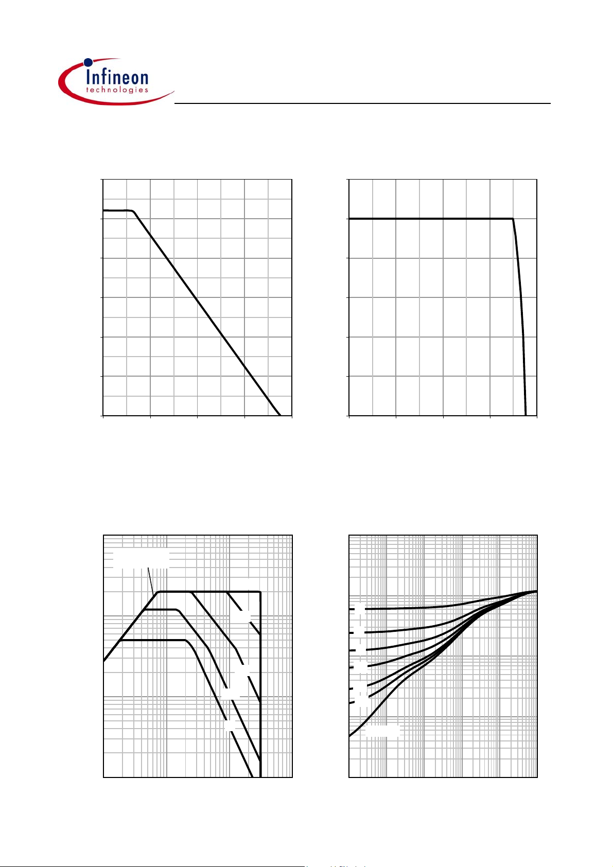
1 Power dissipation 2 Drain current
P
=f(TC) ID=f(TC); VGS≥10 V
tot
BSC022N03S
120
100
80
[W]
60
tot
P
40
20
0
0 40 80 120 160
TC [°C]
60
50
40
30
[A]
D
I
20
10
0
0 40 80 120 160
TC [°C]
3 Safe operation area 4 Max. transient thermal impedance
I
=f(VDS); TC=25 °C; D =0 Z
D
parameter: t
10
10
[A]
D
I
10
10
p
3
1000
limited by on-state
resistance
10 µs
2
100
1
10
0
1
0.1 1 10 100
10
-1
10
0
VDS [V]
10 ms
DC
10
100 µs
1 ms
1
=f(tp)
thJC
parameter: D =tp/T
1
10
0
10
-1
[K/W]
10
thJC
Z
-2
10
-3
10
10
10
2
10
1
0.5
0.2
0.1
0.1
0.05
0.02
0.01
0.01
single pulse
0.001
0 0 0 0 0 0
10
-5
-6
10
-4
tp [s]
10
-3
10
-2
10
-1
Rev. 1.11 page 4 2004-02-05
 Loading...