


查询BGA619供应商
The BGA619 Silicon-Germanium High IP3 Low Noise
Amplifier in PCS Receiver Applications
Features
• Easy-to-use LNA MMIC in 70 GHz f
• Tiny „Green“ P-TSLP-7-1 package (no Lead or Halogen
• Low external component count
• Integrated output DC blocking capacitor, integrated RF
• Three gain steps
• Power off function
• High IP3 in all modes
compounds)
choke on internal bias network
SiGe technology
t
Application Note No. 081
Discrete Semiconductors
6
5
4
7
1
2
3
P-TSLP-7-1
Applications
• Low Noise Amplifier for 1900 MHz PCS wireless frontends (CDMA 2000).
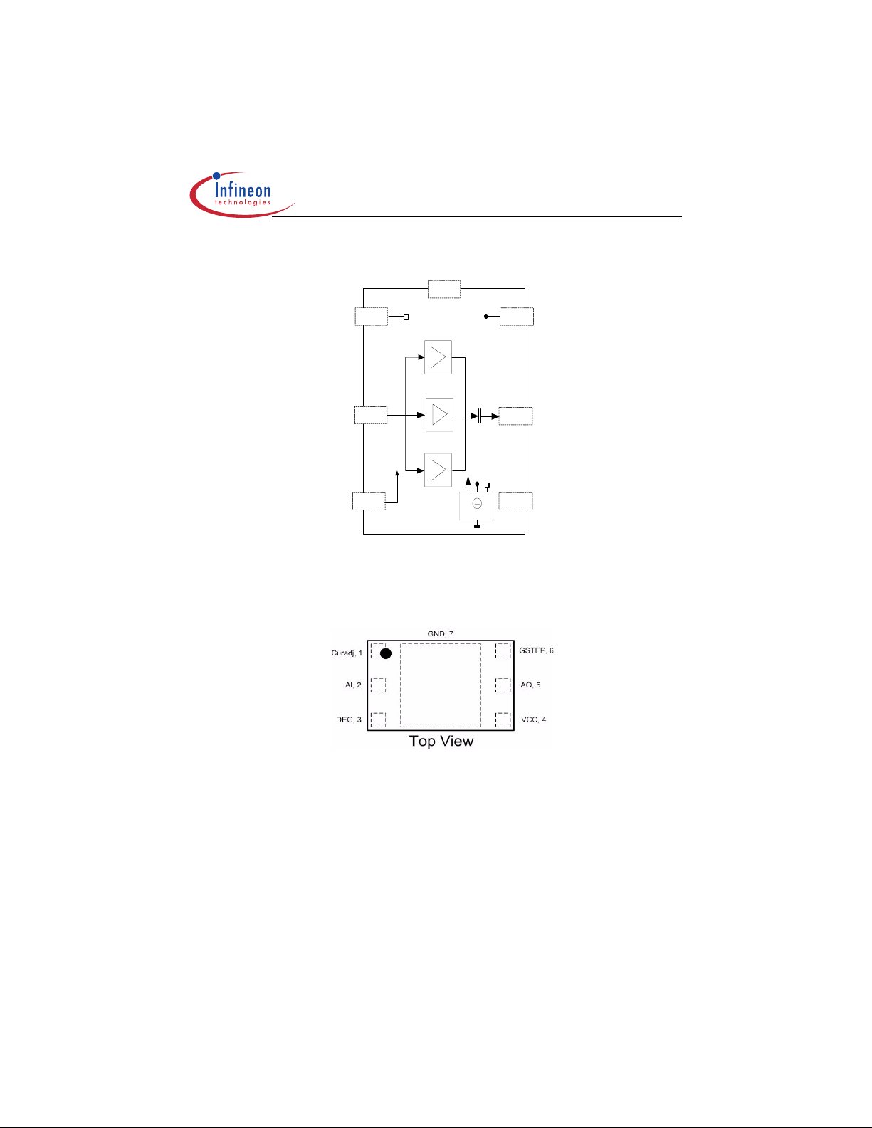
Introduction
The BGA619 is an easy-to-use, low-cost Low Noise Amplifier (LNA) MMIC designed
for use in today’s PCS systems which require excellent linearity in each of several gain
step modes. Based on Infineon’s cost-effective 70 GHz f
Silicon-Germanium (SiGe)
T
B7HF bipolar process technology, the BGA619 offers a 1.5 dB noise figure and 14.9 dB
of gain at 1.96 GHz with a current consumption of 6.5 mA in high gain mode. BGA619
offers impressive IIP3 performance of 7 dBm in High Gain mode, particularly for a threegain step, low-cost, integrated MMIC.
The new LNA incorporates a 50 Ω pre-matched output with an integrated output DC
blocking capacitor. The input is pre-matched, requiring an external DC blocking
capacitor. An integrated, on-chip inductor eliminates the need for an external RF choke
on the voltage supply pin. The operating mode of the device is determined by the voltage
at the GS-pin. An integrated on/off feature provides for low power consumption and
increased stand by time for PCS cellular handsets.
AN081 1 2004-04-19
connected to
CURADJ
1
AI
2
DEG
3
Figure 1 BGA619’s Equivalent Circuit.
paddle
GND
HG
MG
LG
Bias/Gain Select
Application Note No. 081
Discrete Semiconductors
GSTEP
6
AO
5
4
VCC
Figure 2 Pin Connections
AN081 2 2004-04-19
Application Note No. 081
Discrete Semiconductors
Overview
The BGA619 has three gain steps and one off-mode which are used in PCS-band
applications:
• High Gain Mode
• Mid Gain Mode
• Low Gain Mode
• OFF Mode
Mode selection is performed by applying a voltage to pin 6 (GSTEP) as described in
Table 1. The source that generates these mode-select voltages should be able to source
or sink current. Please refer to the BGA619 datasheet for the maximum values of mode
control current.
Table 1 Switching Modes for Gain Steps
Gain Mode Gain Step Input Voltage
[V]
Min Max typ
High Gain 2.2 2.4 65
Mid Gain 1.6 1.8 40
Low Gain 0.9 1.1 8
OFF 0.0 0.3 -35
Current into
GS-pin [µA]
The next table shows the measured performance of each of these gain modes. All
measurement values presented in this application note include losses of both PCB and
connectors - in other words, the reference planes used for measurements are the PCB’s
RF SMA connectors. Noise figure and gain results shown here would improve by 0.2 -
0.3 dB compared to the values shown if PCB losses were extracted.
All measurements are performed at 1960 MHz and at a typical supply voltage of 2.78 V.
AN081 3 2004-04-19
Application Note No. 081
Discrete Semiconductors
Table 2 Performance Overview
Parameter High Gain
Mode
Supply voltage 2.78 V 2.78 V 2.78 V
Supply current 6.5 mA 4.5 mA 2.9 mA
Gain 14.9 dB 2.2 dB -9.5 dB
Noise Figure 1.5 dB 8 dB 16 dB
Input return loss 10.5 dB 8.5 dB 12.5 dB
Output return loss 11.5 dB 13 dB 13 dB
Reverse Isolation 25 dB 21 dB 23 dB
rd
Input 3
1)
2)
3)
order intercept point 7 dBm
-30 dBm per tone, f1=1950 MHz, ∆f=1MHz
-27 dBm per tone, f1=1950 MHz, ∆f=1MHz
-15 dBm per tone, f1=1950 MHz, ∆f=1MHz
1)
Mid Gain
Mode
6.5 dBm
Low Gain
Mode
2)
15 dBm
3)
Board Configuration
The circuit in Figure 3 shows the board configuration for BGA619 LNA. The Bill of
materials for the application board can be found in Table 3.
Figure 3 PCB board configuration
N1
R1
C3
RFin
L1
C1
Curadj, 1
AI, 2
DEG, 3 Vcc, 4
AN081 4 2004-04-19
GSTEP, 6
GND, 7
AO, 5
C4 C5
C6
GS
C2
RFout
L2
Vcc
Application Note No. 081
Discrete Semiconductors
Table 3 Bill of materilal
Name Value Package Manufacturer Function
R1 15 kΩ 0402 various bias resistance; set device
current
L1 3.3 nH 0402 various LF trap & input matching; L1
and C1 provide low-frequency
trap to increase input IP3
L2 4.7 nH 0402 various output matching
C1 10 nF 0402 various LF trap for IP3 enhancement
C2 10 pF 0402 various output DC block; optional
because DC block is integrated
C3 10 pF 0402 various input DC block
C4 10p 0402 various control voltage filtering -
OPTIONAL, depends on actual
user implementation
C5 1 nF 0402 various control voltage filtering -
OPTIONAL, depends on actual
user implementation
C6 1 nF 0402
C7 0402
N1 BGA619 P-TSLP-7-1 Infineon SiGe LNA with gain-steps
various
various
supply filtering, depends on
actual user implementation
supply filtering OPTIONAL, depends on actual
user implementation
The application board is made of 3 layer FR4 material (see Figure 4). The top view can
be seen in Figure 5 and the bottom view in Figure 6. Pictures of the board can be found
in Figure 7 (complete board) and Figure 8 (close-in photograph, where BGA619 and
surrounding elements can be found in detail).
AN081 5 2004-04-19
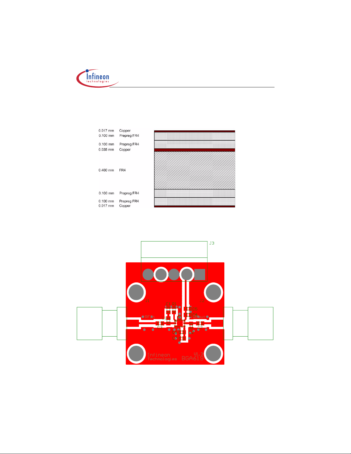
Figure 4 Application board; board construction
Figure 5 Application board; top view
Application Note No. 081
Discrete Semiconductors
AN081 6 2004-04-19

Figure 6 Application board; bottom view
Application Note No. 081
Discrete Semiconductors
Figure 7 Foto of Application board
AN081 7 2004-04-19

Figure 8 Scanned image of PCB, Close-In shot
Application Note No. 081
Discrete Semiconductors
AN081 8 2004-04-19

Application Note No. 081
Discrete Semiconductors
The power supply connector
Figure 9 shows the pinning of the power supply connector needed for powering the test
board.
Figure 9 Power Supply Connector
For measurment graphs please refer to the next pages.
AN081 9 2004-04-19

Figure 10 Noise Figure High Gain Mode
Noise Figure NF = f(f)
V
= 2.78V, I
CC
= 6.5mA
CC
1.8
1.7
1.6
1.5
NF [dB]
1.4
1.3
1.2
1.8 1.85 1.9 1.95 2 2.05 2.1
Frequency [GHz]
Figure 11 Gain High Gain Mode
Application Note No. 081
Discrete Semiconductors
Power Gain |S21| = f(f)
V
= 2.78V, I
CC
= 6.5mA
CC
15.2
15.1
15
14.9
14.8
Power Gain [dB]
14.7
14.6
14.5
1.8 1.85 1.9 1.95 2 2.05 2.1
Frequency [GHz]
AN081 10 2004-04-19

Figure 12 Return Loss High Gain Mode
Matching |S11|, |S22| = f(f)
V
= 2.78V, I
CC
= 6.5mA
CC
−4
−6
−8
−10
| [dB]
22
−12
|, |S
11
|S
−14
−16
−18
−20
1.8 1.85 1.9 1.95 2 2.05 2.1
S
22
Frequency [GHz]
Figure 13 Reverse Isolation High Gain Mode
Application Note No. 081
Discrete Semiconductors
S
11
Reverse Isolation |S12| = f(f)
V
= 2.78V, I
CC
= 6.5mA
CC
−20
−21
−22
−23
−24
−25
| [dB]
12
|S
−26
−27
−28
−29
−30
1.8 1.85 1.9 1.95 2 2.05 2.1
Frequency [GHz]
AN081 11 2004-04-19

Figure 14 Noise Figure Mid Gain Mode
Noise Figure NF = f(f)
V
= 2.78V, I
CC
= 4.5mA
CC
8.4
8.3
8.2
8.1
8
NF [dB]
7.9
7.8
7.7
7.6
1.8 1.85 1.9 1.95 2 2.05 2.1
Figure 15 Gain Mid Gain Mode
Application Note No. 081
Discrete Semiconductors
Frequency [GHz]
Power Gain |S21| = f(f)
V
= 2.78V, I
CC
= 4.5mA
CC
2.6
2.5
2.4
2.3
2.2
2.1
2
Power Gain [dB]
1.9
1.8
1.7
1.6
1.8 1.85 1.9 1.95 2 2.05 2.1
Frequency [GHz]
AN081 12 2004-04-19

Figure 16 Return Loss Mid Gain Mode
Matching |S11|, |S22| = f(f)
V
= 2.78V, I
CC
= 4.5mA
CC
−4
−6
−8
−10
| [dB]
22
−12
|, |S
11
|S
−14
−16
−18
−20
1.8 1.85 1.9 1.95 2 2.05 2.1
Frequency [GHz]
Figure 17 Reverse Isolation Mid Gain Mode
Application Note No. 081
Discrete Semiconductors
S
11
S
22
Reverse Isolation |S12| = f(f)
V
= 2.78V, I
CC
= 4.5mA
CC
−15
−16
−17
−18
−19
−20
| [dB]
12
|S
−21
−22
−23
−24
−25
1.8 1.85 1.9 1.95 2 2.05 2.1
Frequency [GHz]
AN081 13 2004-04-19

Figure 18 Noise Figure Low Gain Mode
Noise Figure NF = f(f)
V
= 2.78V, I
CC
= 2.9mA
CC
17
16.8
16.6
16.4
16.2
16
NF [dB]
15.8
15.6
15.4
15.2
15
1.8 1.85 1.9 1.95 2 2.05 2.1
Frequency [GHz]
Figure 19 Gain Low Gain Mode
Application Note No. 081
Discrete Semiconductors
Power Gain |S21| = f(f)
V
= 2.78V, I
CC
= 2.9mA
CC
−8
−8.5
−9
−9.5
Power Gain [dB]
−10
−10.5
−11
1.8 1.85 1.9 1.95 2 2.05 2.1
Frequency [GHz]
AN081 14 2004-04-19

Figure 20 Return Loss Low Gain Mode
Matching |S11|, |S22| = f(f)
V
= 2.78V, I
CC
= 2.9mA
CC
−4
−6
−8
−10
| [dB]
22
−12
|, |S
11
|S
−14
−16
−18
−20
1.8 1.85 1.9 1.95 2 2.05 2.1
S
22
Frequency [GHz]
Figure 21 Reverse Isolation Low Gain Mode
Application Note No. 081
Discrete Semiconductors
S
11
Reverse Isolation |S12| = f(f)
V
= 2.78V, I
CC
= 2.9mA
CC
−15
−16
−17
−18
−19
−20
| [dB]
12
|S
−21
−22
−23
−24
−25
1.8 1.85 1.9 1.95 2 2.05 2.1
Frequency [GHz]
AN081 15 2004-04-19

Application Note No. 081
Discrete Semiconductors
AN081 16 2004-04-19

Application Note No. 081
Discrete Semiconductors
AN081
Revision History: 2004-04-19 v1.0
Previous Version:
Page Subjects (major changes since last revision)
For questions on technology, delivery and prices please contact the Infineon
Technologies Offices in Germany or the Infineon Technologies Companies and
Representatives worldwide: see our webpage at http://www.infineon.com
Edition 2004-04-19
Published by Infineon Technologies AG,
St.-Martin-Strasse 53,
D-81541 München
© Infineon Technologies AG 1999.
All Rights Reserved.
Attention please!
The information herein is given to describe certain components and shall not be considered as warranted characteristics.
Terms of delivery and rights to technical change reserved.
We hereby disclaim any and all warranties, including but not limited to warranties of non-infringement, regarding
circuits, descriptions and charts stated herein.
Infineon Technologies is an approved CECC manufacturer.
Information
For further information on technology, delivery terms and conditions and prices please contact your nearest Infineon Technologies Office in Germany or our Infineon Technologies Representatives worldwide (see address list).
Warnings
Due to technical requirements components may contain dangerous substances. For information on the types in
question please contact your nearest Infineon Technologies Office.
Infineon Technologies Components may only be used in life-support devices or systems with the express written
approval of Infineon Technologies, if a failure of such components can reasonably be expected to cause the failure
of that life-support device or system, or to affect the safety or effectiveness of that device or system. Life support
devices or systems are intended to be implanted in the human body, or to support and/or maintain and sustain
and/or protect human life. If they fail, it is reasonable to assume that the health of the user or other persons may
be endangered.
AN081 17 2004-04-19
 Loading...