

A
查询BGA430供应商
pplications Note No. 074
Silicon Discretes
A 35 dB Gain-Sloped LNB I.F. Amplifier for Direct Broadcast Satellite
Television Applications using the BGA430 & BGB540 Silicon MMICs
Gain = 32 – 37 dB from 950 – 2150 MHz (positive gain slope)
•
Low Power Consumption: 40mA at +5.0 Volts
•
Exceptionally low Noise Figure: less than 3 dB
•
Low Cost, Low Parts Count
•
High Reverse Isolation
•
Output Compression point: +1 dBm minimum
•
(May be increased with higher DC bias level)
Suitable for European, Asian & North American DBS
•
LNB I.F. Amplifier Chains for 950 – 1450 and 950 – 2150 MHz
1. Overview
Infineon’s BGA430 Broad Band High Gain
Low Noise Amplifier and BGB540 Active
Biased Transistor are shown in an
Intermediate-Frequency (“I.F.”) amplifier
application targeted for the I.F. chains of
European, Asian and North American DirectBroadcast Satellite (DBS) Low Noise Block
Amplifier / Downconverters (LNBs).
A summary of key performance parameters for
the complete LNB I.F. Amplifier is given in Table
1 to the right. The reader is referred to
Appendix A on page 21 for complete electrical
data including minimum, maximum, mean value,
and standard deviation for the lot of Printed
Circuit Boards (PCBs) tested. Appendix B on
page 22 gives information on performance over
the –40 to +85 °C temperature range.
Section 2 of this applications note provides a
brief description of the BGA430 and BGB540
MMICs. Section 3 gives some general Direct
Broadcast Satellite system information, and is
included to provide a general background.
Section 4 provides details on the PC Board
used, including photos, a Bill of Material (BOM)
and a PCB cross-sectional diagram. Section 5
describes using the BGA430 MMIC as a standalone DBS I.F. Amplifier block, and covers
design issues unique to BGA430. Section 6
addresses the question “why might one want a
positive gain slope I.F. Amplifier” and Section 7
gives measurement results on the complete
gain-sloped amplifier using both BGA430 &
BGB540.
Table 1. Typical performance for the
complete BGA430+BGB540 LNB I.F.
Amplifier.
Conditions: Temperature=25°C, V=5.0 Volts, n=25 units,
=50Ω, network analyzer source power = -40 dBm
Z
S=ZL
Parameter
Input Return Loss, dB
Gain, dB
Reverse Isolation, dB
Output Return Loss, dB
Noise Figure, dB
Output P
Input IP3, dBm
1dB
Please note that the reference planes for all
measurement data shown in Table 1 are at the
PC board’s SMA RF connectors; e.g. no PCB
loss is extracted from the numbers given.
Frequency, MHz
950 1450 2150
26.0 27.3 12.0
33.0 37.2 37.2
>50 >50 >50
13.7 13.4 13.1
2.4 2.4 2.6
, dBm
+1.7 +4.9 +7.9
-20.8 -22.5 -18.9
AN 074 Rev E 1 / 24 19-November-2002
A
pplications Note No. 074
Silicon Discretes
2. Description of BGA430 and BGB540
The BGA430 is a three-stage, 50 ohm, internally
matched, unconditionally stable MMIC fabricated
in Infineon’s well-proven, consistent and costeffective 25 GHz transition frequency (f
) B6HF
T
bipolar process. The BGA430 only requires
three external elements – input / output DC
blocking capacitors, and a single decoupling
capacitor on the power supply pin. Depending
on the particular LNB performance
requirements, the BGA430 may be used as a
stand-alone I.F. amplifier block, or together with
the BGB540.
The BGB540 is an unmatched, active-biased RF
transistor produced in the 45 GHz f
B6Hfe
T
bipolar process. B6Hfe, derived from B6HF, is a
more advanced process with higher achievable
gains and lower noise figures. BGB540 uses an
internal current mirror for DC biasing. This
approach achieves some reduction in external
component count due to elimination of a number
of external DC bias circuit elements, while still
preserving the flexibility inherent in a fully
discrete transistor. The device bias current may
be adjusted via a single external resistor.
Furthermore, the internal current-mirror, being
located on the same chip as the RF transistor
cell, has excellent “thermal tracking” of the RF
transistor cell, providing for a more stable DC
operating point over temperature. The BGB540
preserves the cost-advantages of the simple 4pin industry-standard SOT343 package.
A block diagram and package drawing for the
BGA430 and BGB540 are given in Figures 1 &
2, respectively. Note that for the BGB540, the
emitter areas of the current-mirror transistor cell
and the RF transistor cell are in the ratio of 1:10.
To set DC bias current for the BGB540, one
injects a current into pin 4, and the current
drawn by the RF transistor cell is 10 times the
current injected into pin 4, by virtue of the
current-mirror principle. The simplest DC bias
configuration for BGB540 involves using just a
single resistor between the power supply and
pin 4 – no RF choke or decoupling capacitor is
required on pin 4. The value of this bias resistor
– referred to as “ R
“ – required for a given
BIAS
device current can be determined from curves
given in the BGB540 datasheet. For lower
operating currents, the value of R
large, and therefore R
in series with the
BIAS
BIAS
becomes
power supply voltage behaves as a near-ideal
constant-current source. Otherwise, the
BGB540 is treated like a standard RF transistor,
with the normal procedures for impedance
matching, stability analysis, etc. being used.
Figure 1. BGA430 Block Diagram and
Package (SOT363).
4
GND2
3
RFout
5
GND1
2
GND1
6
RFin
BGA430 (B6HF) V
= 6.5 V, I
MAX
Bias
MAX
1
Vcc
= 35 mA
Figure 2. BGB540 Block Diagram and
Package (SOT343).
BFP540
C
Pin 3
Bias
Pin 4
1/10 BFP540
Base
Pin 1
BGB 540 B6HFe
VCE
= 4.5 V I
MAX
C MAX
= 80 mA
Emitter
Pin 2
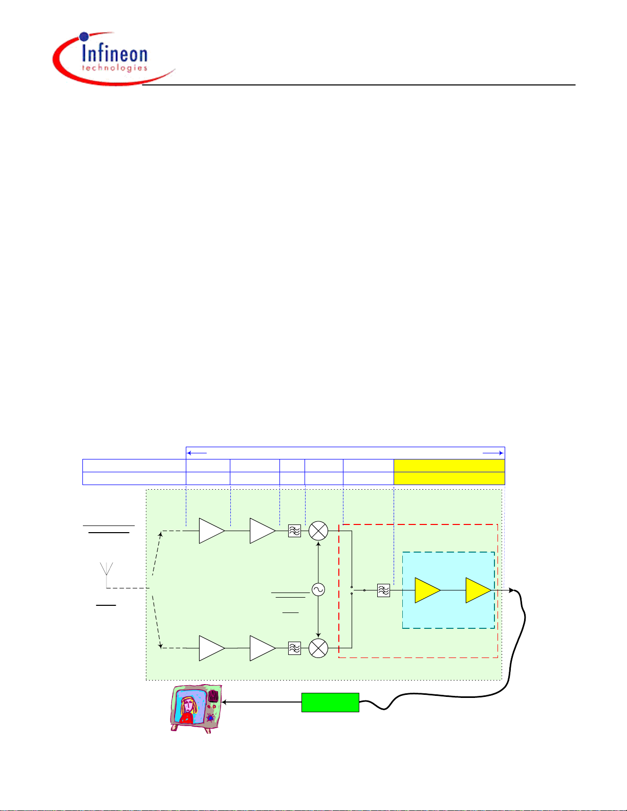
3. General DBS System Information
A generic block diagram of a Direct Broadcast
Satellite Low Noise Block Amplifier /
Downconverter (LNB) is given in Figure 3 on
page 3. LNBs produced for the Direct Broadcast
Satellite consumer electronics market are
extraordinarily cost-sensitive, and cost issues
are usually the primary consideration in the LNB
design process.
A broadcast signal in the 12 GHz range is
transmitted from an orbiting satellite towards the
Earth’s surface. There are two orthogonal parts
AN 074 Rev E 2 / 24 19-November-2002
A
pplications Note No. 074
Silicon Discretes
of the composite signal – a vertically polarized
component, and a horizontally polarized
component. The two polarizations enable more
efficient use of the available bandwidth and
power. (The isolation between “vertical” and
“horizontal” radio signals permits a greater
number of channels to be simultaneously
broadcast within the available bandwidth than
would otherwise be expected.) The satellite’s
transmitted signal is received by an earth-based
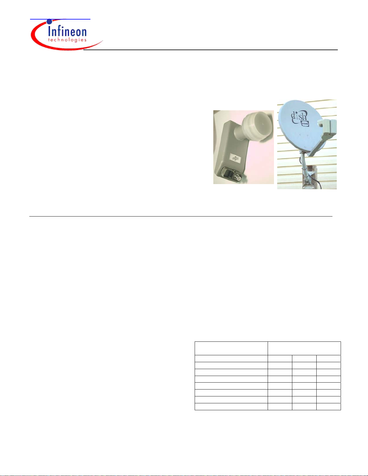
antenna like that shown in the photo on page 1.
The signal is focused by the parabolic “dish”
antenna onto a waveguide integrated into the
LNB. The received signal travels a short
distance down the waveguide until reaching a
waveguide-to-microstripline transition that
carries the signal onto the LNB circuit board
assembly.
The LNB must be able to receive channels on
both the vertically and horizontally polarized
signals – and one way to do this is to have
essentially two different receiver front-ends as
shown in Figure 3 below.
Figure 3. Generic Block Diagram, "Single Output" Direct
Broadcast Satellite Television Block Downconverter (DBS LNB)
Cascaded Gain: approximately 55 - 60 dB; Cascaded Noise Figure: approximately 1 dB
Approximate Gain, dB =>
Approximate Noise Figure, dB =>100.5
0.7
12
-1.5
1.5
Various approaches and switching schemes are
employed in different LNB designs to enable the
end user(s) to select between channels riding on
either the horizontally or vertically polarized
signals. Each approach has its own unique cost
and performance trade-offs. Optimizing LNB
architectures to achieve performance
requirements while continuously reducing cost
as new, higher-performance and lower cost
semiconductor devices become available is a
challenging task.
A further complication to the switching
requirements is added if one wishes to have a
“dual output LNB” – e.g. an LNB that can drive
two different set-top boxes and television sets
simultaneously, allowing each TV to display a
different channel. (“Quad output” LNBs are also
available). One possible switching scheme for a
“single output LNB” is shown in Figure 3. Note
that the vertical / horizontal switching is done at
the I.F. Amplifier block. The BGA430 and
BGB540 are shown in the shaded I.F. Amplifier
section.
-10 to +8
7 to 12
- 4 30 to 45
4
3 to 7
LNB
U.S., Japan, Korea,
Latin America
11.45 - 12.75 GHz
(depending on region)
Horizontal
Polarization
LNA LNA
(Passive or Active)
BPF
Mixer
(Components in Shaded Area)
I.F. Amplifier
Local Oscillator
(DRO)
U.S., Japan, Korea,
Latin America:
Europe
10.7 - 12.75 GHz
(Two L.O.'s required for
full coverage)
Vertical
Polarization
AN 074 Rev E 3 / 24 19-November-2002
LNA LNA
in 10.5 - 11.25 GHz range
Audio + Video
to TV set
Europe:
10.6 GHz or
9.75 + 10.6 GHz
(dual DRO)
BPF
Mixer
(Passive or Active)
"Set Top Box"
(Channel Selector,
Demodulator, etc.)
(Vert. / Hor.)
Switch
BPF
Intermediate Frequency ("I.F.")
950 - 1450 MHz (North America)
950 - 2150 MHz (Europe, Asia)
IF Amp IF Amp
BGA430 + BGB540
75 ohm Coaxial Cable
To Set-Top Box
(75 ohm system)
RG-6, RG-6/U

A
pplications Note No. 074
Silicon Discretes
After the waveguide to microstrip transition, the
signals enter a PC Board assembly. The signal
is amplified in two or more low noise amplifier
(LNA) stages and then hits a band pass filter.
The LNAs provide enough gain to boost the
level of the received signal such that the overall
receiver noise figure is dominated by the LNA
block itself. The LNA stages must have enough
gain and a sufficiently low noise figure to
minimize the noise floor for the entire receive
chain. Achieving enough gain and a low enough
noise figure at 12 GHz is costly, and anything
that can reasonably be done to relax the
requirements on the LNA section will reduce
cost.
The LNA is then followed by a band pass filter
(BPF) which provides for some rejection of out –
of-band signals and noise, as well as image
rejection. The amplified and filtered signal then
enters the mixer stage.
The types of simple, inexpensive mixers likely to
be used in an LNB will usually convert both the
desired input signal (12 GHz in this case) and an
undesired “image” frequency (10 GHz) to the
intermediate frequency (1 GHz for this example).
The band pass filter in front of the mixer stage
can attenuate any undesired signals or noise
present at the 10 GHz image frequency before it
hits the mixer stage, preventing the undesired
image from being down-converted on top of the
desired, down-converted 12 GHz input signal.
At present, most LNB manufacturers use one of
three main types of mixers:
1. GaAs FET used as a simple active mixer
2. GaAs FET with no DC bias applied ( “FET
resistive mixer”)
3. Schottky Diode based mixer
Some references for mixers are given in [1] and
[2] at the end of this applications note.
The FET active mixer will usually have
“conversion gain” while the FET resistive mixer
or Schottky diode mixers have “conversion loss”.
Conversion gain or loss is simply the ratio of the
amplitudes of the down-converted output I.F.
signal to the RF input signal. A poor noise figure
in the mixer stage, as well as high conversion
loss, places additional demands (and cost) on
both the LNA block up front, as well as the I.F.
amplifier which follows.
The down-converted I.F. signal undergoes
further band pass filtering and then is amplified
in the I.F. amplifier block. The I.F. amplifier is
the focus of this applications note, and is the
primary point of discussion regarding the
BGA430 and BGB540 Silicon MMICs. The I.F.
amplifier boosts the signal up to a reasonable
input level for the set top box. It is worth noting
that the system impedance in this area is 75
ohms, not 50 ohms, and that the coaxial cable
typically used (RG-6, RG-6/U or sometimes RG-
59) is very low cost, and has a relatively high
attenuation per unit length a the intermediate
frequency. Furthermore, the attenuation of the
cable increases with increasing frequency –
coaxial cable loss at 2150 MHz is higher than
cable loss at 950 MHz. Herein lies the reason
for designing an I.F. amplifier with a gain
slope that increases with increasing
frequency – this positive gain slope in the
I.F. amp will help to compensate out the
negative gain slope of the coaxial cable and
other RF front-end blocks.
4. Information on Printed Circuit Board
The PC board used in this applications note was
simulated within and generated from the
Eagleware GENESYS
®
[3] software package.
After simulations, CAD files required for PCB
fabrication, including Gerber 274X and Drill files,
were created within and output from GENESYS.
Photos of the PC board are provided in Figures
4, 5 and 6. A cross-sectional diagram is given
in Figure 7. A schematic diagram and a Bill Of
Material (BOM) for the complete BGA430 +
BGB540 I.F. Amplifier are given in Figures 8
and 9, respectively. The PC Board material
used is standard FR4. Note that each MMIC
may be tested individually; capacitor C3 (see
schematic) may be positioned to “steer” the RF
from the BGA430 output to the SMA connector
on the bottom of the PCB, or, C3 may be used
to link the track from this same RF connector to
the input of the BGB540. When testing the
AN 074 Rev E 4 / 24 19-November-2002
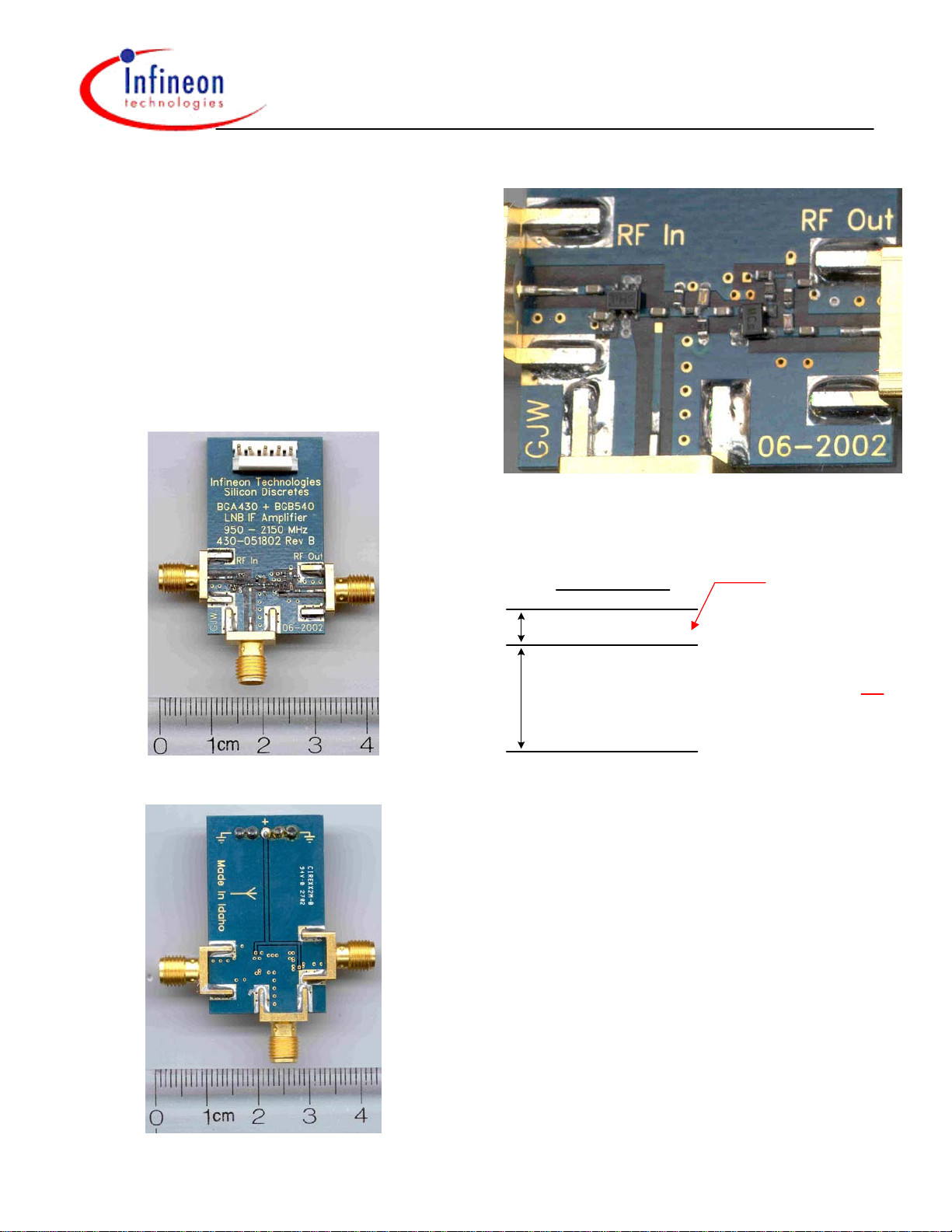
A
pplications Note No. 074
Silicon Discretes
BGB540 stage alone, a zero-ohm “jumper”
needs to be used in place of R2. The total PCB
area consumed for the entire BGA430 +
BGB540 I.F. Amplifier is approximately 0.585 x
0.180 inch / 14.9 x 4.6 mm, or approximately 70
2
mm
. The total component count, including
both Silicon MMICs, is 16. Note that PCB area
and component count may be reduced markedly
if the end user is able to satisfy his or her I.F.
amplifier requirements by using the BGA430 as
a stand-alone part. The next section describes
the BGA430 as a stand-alone I.F. amplifier.
Figure 4. Top View of I.F. Amp PC Board.
Figure 6. Close-In Shot of PCB. BGA430 on
left, BGB540 on Right.
Figure 7. Cross-Section Diagram of I.F.
Amplifier Printed Circuit Board.
PCB CROSS SECTION
THIS SPACING CRITICAL !
Figure 5. Bottom View of I.F. Amp PC Board
0.010 inch / 0.254 mm
0.031 inch / 0.787 mm ?
LAYER FOR MECHANICAL RIGIDITY OF PCB, THICKNESS HERE NOT
CRITICAL AS LONG AS TOTAL PCB THICKNESS DOES NOT EXCEED
0.045 INCH / 1.14 mm (SPECIFICATION FOR TOTAL PCB THICKNESS:
0.040 + 0.005 / - 0.005 INCH; 1.016 + 0.127 mm / - 0.127 mm )
TOP LAYER
INTERNAL GROUND PLANE
BOTTOM LAYER
5. Using the BGA430 as a Stand-Alone I.F.
Amplifier Block
Provided that BGA430 gain magnitude, gain
curve and output power are adequate for the
user’s LNB system requirements, BGA430 may
be used as a very low-parts-count, low-cost
stand-alone LNB I.F. amplifier over the 950 –
2150 MHz range. Note that only 3 external
elements are typically required with BGA430:
1) an input DC blocking capacitor 2) an output
DC blocking capacitor 3) an RF bypass / RF
decoupling capacitor on the V
pin (Pin 1).
CC
Table 2 on page 8 summarizes the BGA430’s
typical performance and Figures 11 – 15 give
network analyzer screen shots of input / output
match, gain, and (continued on page 7)
AN 074 Rev E 5 / 24 19-November-2002
A
pplications Note No. 074
Silicon Discretes
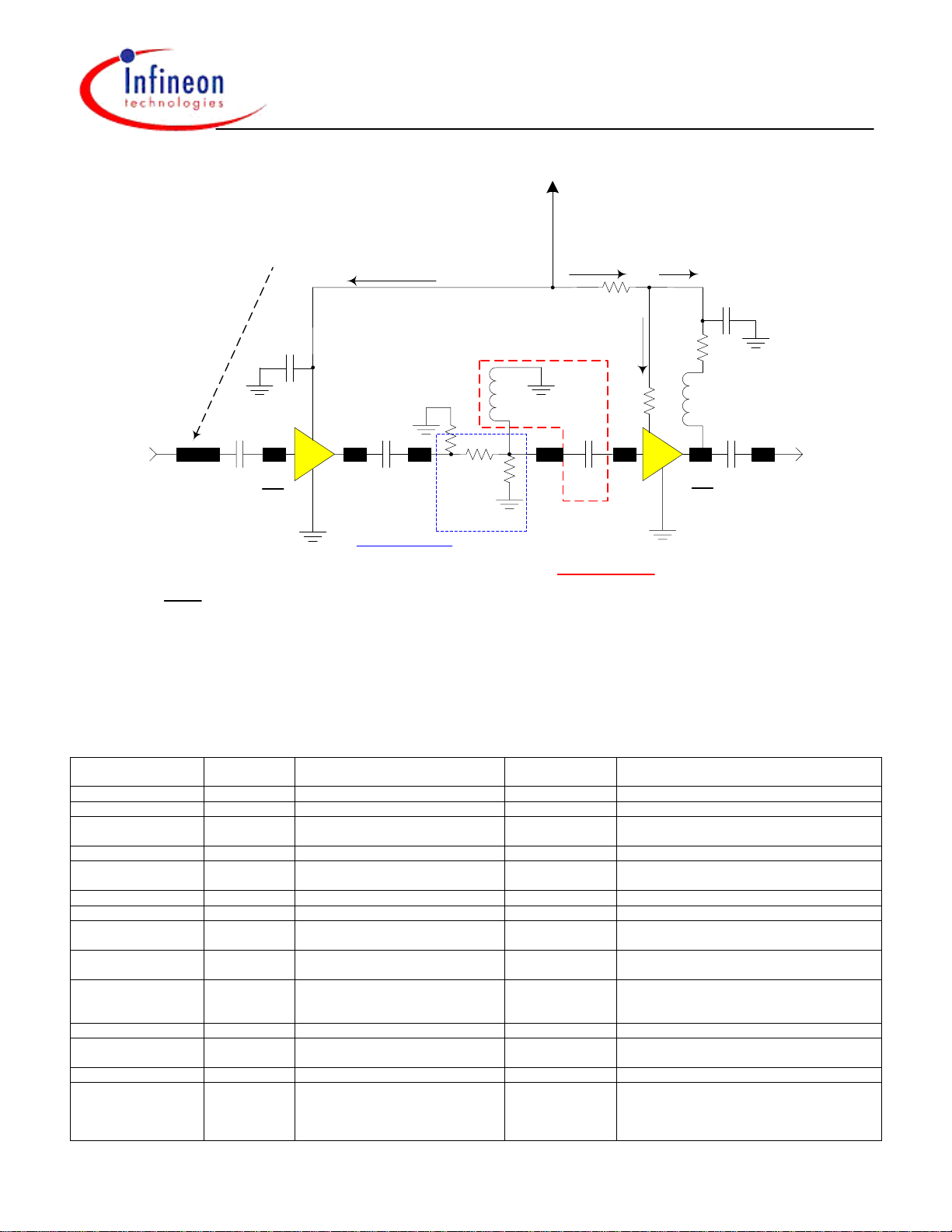
Figure 8. Schematic Diagram of Complete BGA430 + BGB540 LNB I.F. Amplifier
J3
+5.0 Volts
(Total Current Draw = 39.9 mA)
Black Rectangles = Microstriplines on PCB
(PCB Track or Trace)
22.9 mA
17.0 mA
30 ohms
15.45 mA
R6
C6
22 pF
1.55 mA
C2
22 pF
R1
300 ohms
L1
3.0 nH
R4
2K
(R Bias)
J1 J2
RF Input
950 - 2150 MHz
C1
22 pF
IC1
C3
22 pF
R2
18 ohms
R3
300 ohms
C4
1.5 pF
MMIC
Notes:
BGA430
B6HF
Purpose of Pad :
3 dB Pad
1) Gain Reduction (especially at lower end of band)
2) Provide good input termination for HPF
High Pass Filter
Butterworth
= 1860 MHz
f
C (3 dB)
Purpose of HPF :
Adjust overall gain
slope of cascade
43 ohms
L2
4.7 nH
IC2
MMIC
BGB540
B6HFe
R5
C5
22 pF
RF Output
1) Using C4 as both a DC block and as a Highpass Filter element enables the elimination of one capacitor
2) Bias current of Stage 2 (BGB540 MMIC) can be increased or decreased to vary overall output compression point
3) Stage 1 (BGA430) requires careful attention to proper grounding !
Figure 9. Bill Of Material (BOM) for Complete BGA430 + BGB540 LNB I.F. Amplifier
REFERENCE
DESIGNATOR
VALUE
MANUFACTURER
C1, C3, C5 22 pF VARIOUS 0402 DC BLOCK
C2, C6 22 pF VARIOUS 0402 RF BYPASS
C4 1.5 pF VARIOUS 0402 DC BLOCK & HIGH PASS FILTER
L1 3.0 nH MURATA LQP15M 0402 HIGH PASS FILTER FUNCTION
L2 4.7 nH MURATA LQP15M 0402 “RF CHOKE” / DC FEED FOR BGB540,
R1, R3 300 OHMS VARIOUS 0402 FOR 3 dB ATTENUATOR PAD
R2 18 OHMS VARIOUS 0402 FOR 3 dB ATTENUATOR PAD
R4 2K VARIOUS 0402 R
R5 43 OHMS VARIOUS 0402 RF STABILITY AND OUTPUT MATCH FOR
R6 30 OHMS VARIOUS 0402 DROP 5V SUPPLY TO ~ 4.5V. MAY BE
IC1 - INFINEON TECHNOLOGIES SOT363 BGA430 Si MMIC, B6HF PROCESS
IC2 - INFINEON TECHNOLOGIES SOT343 BGB540 ACTIVE BIASED TRANSISTOR
J1, J2 - JOHNSON 142-0701-841 - RF INPUT / OUTPUT CONNECTOR
J3
-
AMP 5 PIN HEADER
MTA-100 SERIES
P/N 640456-5 OR
641215-5 (GOLD PLATING)
CASE SIZE
FUNCTION
FUNCTION
INFLUENCES BGB540 OUTPUT MATCH
FOR IC2 (BGB540 MMIC) - SETS
BIAS
DEVICE CURRENT)
IC2 (BGB540)
OMITTED IF MAXIUM RATINGS OF IC2
ARE NOT EXCEEDED.
MMIC, B6HFe PROCESS
-
DC CONNECTOR
PINS 1, 2, 4, 5 = GROUND
PIN 3 = V
CC
AN 074 Rev E 6 / 24 19-November-2002
A
pplications Note No. 074
Silicon Discretes
reverse isolation. Note that all of these results
are taken in a 50 ohm system, and that results in
a 75 ohm system will differ slightly.
Circuit Design Issues Relevant to BGA430:
1) proper device grounding !!
2) proper bypassing of the V
CC
pin !
The BGA430 is an extremely high gain device
(>30 dB @ 1 GHz) contained within a single
SMT package. As a result, casual or sloppy
PCB layout techniques which add undesired
parasitic inductance between BGA430 ground
leads and PCB ground plane will add enough
feedback to adversely alter the BGA430’s gain
and return loss. In cases of extremely poor
grounding, sufficient feedback will be present to
enable either gain “peaking” or even an
oscillation. In addition, the V
pin (Pin 1) needs
CC
to be bypassed with a capacitor that, with its
self-inductance taken into account,
approximates a short-circuit in the 1 to 2 GHz
range. Generally a 0603 or 0402 case-size chip
capacitor in the range of 15 – 22 pF is sufficient.
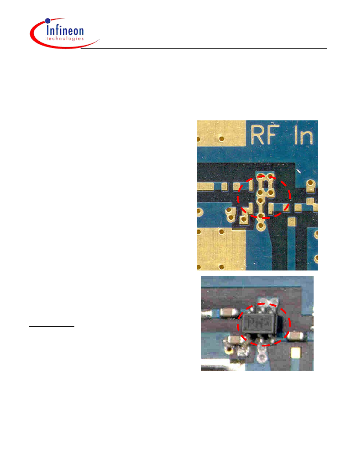
A photo of a bare I.F. Amp PC board is shown in
Figure 10, with a close-in view of the BGA430
mounting area. Note that seven (7) ground vias
are provided for the BGA430 ground pins,
including three ground vias located immediately
underneath the device. Note the two ground
holes provided for the bypass capacitor C2
(22pF) on the BGA430 V
proximity of C2 to the V
pin, and the close
CC
pin.
CC
To summarize:
• The user must avoid any additional parasitic
ground inductance between BGA430 ground
pins and PCB ground plane. A sufficient
number of ground vias need to be provided
and these vias should be placed as close to
the BGA430 as possible.
• BGA430 V
pin (Pin 1) must be bypassed
CC
carefully, and the bypass capacitor used
must have its “cold” side well-grounded.
If these two suggestions are carefully followed, a
low-cost, single device solution may be used for
some I.F. amplifier designs, requiring only 3
external elements.
Figure 10. BGA430 Mounting Position on PC
Board. Compare unpopulated (above) to
populated (below) PCB images. Note
locations and number of ground vias near
BGA430 MMIC. Pin 1 (V
) is pad at lower left.
CC
It needs to be pointed out that the BGA430 is
designed to operate at a nominal supply voltage
of +5 volts, with a current draw of approximately
23mA. However, if a higher output compression
point is desired, the BGA430 may be safely run
up to 6.5 volts, and maximum safe current is
35mA. If an adjustable output voltage regulator
AN 074 Rev E 7 / 24 19-November-2002
A
pplications Note No. 074
Silicon Discretes
is used in the LNB, and if a higher output power
is required of the BGA430 than is available at
the 5V, 23mA condition, the user has the option
of simply cranking up the BGA430 supply
voltage.
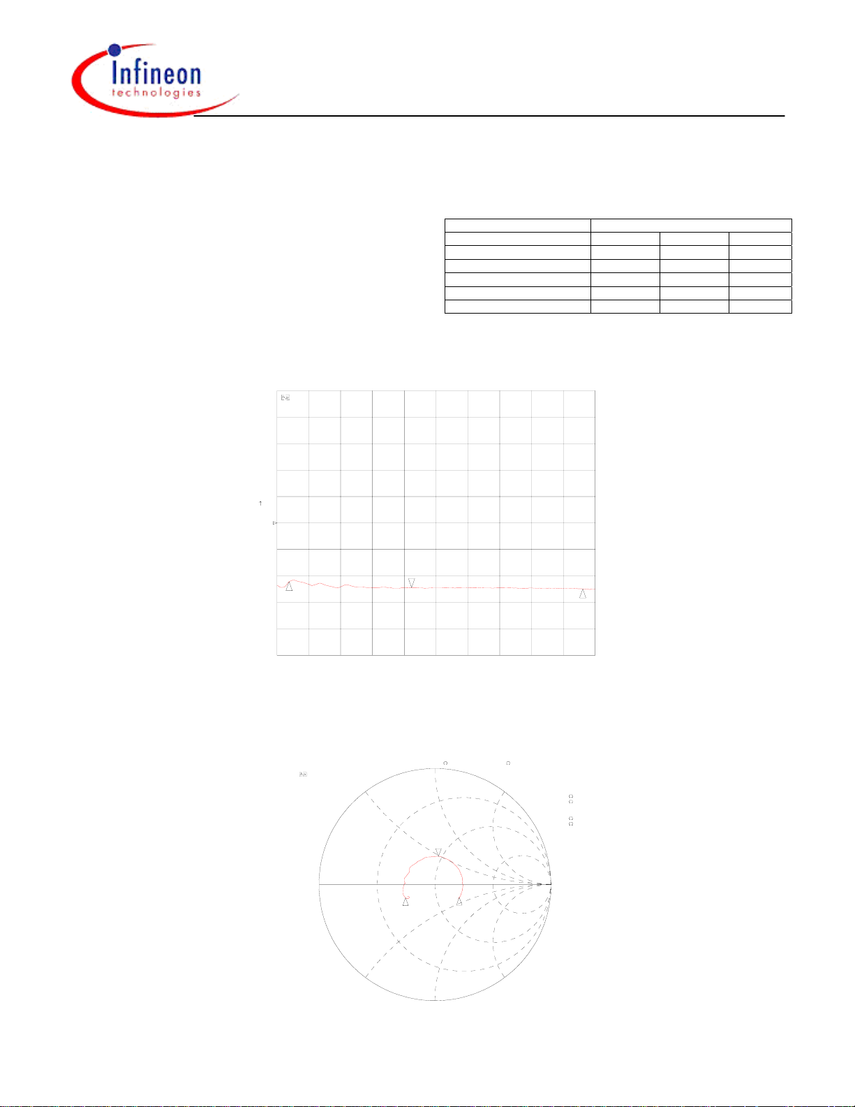
Figure 11. Stand-Alone BGA430 Amp, Input Return Loss.
CH1 S11 log MAG 5 dB/ REF 0 dB
PRm
Cor
Del
Avg
16
Smo
Table 2. Summary of stand-Alone BGA430
LNB I.F. Amplifier Performance.
Conditons: Temperature = 25°C, V = 5.0 Volts, PCB = Infineon
P/N 430-051802 Rev B, Z
power = -40 dBm.
Parameter Frequency, MHz
950 1450 2150
Input Return Loss, dB 11.1 12.2 12.4
Gain, dB 33.4 33.2 27.8
Reverse Isolation, dB 40.5 42.5 46.1
Output Return Loss, dB 13.7 13.4 13.1
Output P
31 Jul 2002 00:56:05
, dBm +3.2 +3.9 +3.2
1dB
2_:-12.193 dB
1 450.000 000 MHz
1_:-11.101 dB
950 MHz
3_:-12.448 dB
2.15 GHz
=50 Ω, network analyzer source
S=ZL
1
START 900.000 000 MHz STOP 2 200.000 000 MHz
2
3
Figure 12. Stand-Alone BGA430 Amp, Input Return Loss, Smith Chart.
Reference Plane = PCB Input SMA Connector.
CH1 S11 1 U FS
PRm
Cor
Del
Avg
16
Smo
2_: 47.119
1
31 Jul 2002 00:56:16
24.293 2.6664 nH
1 450.000 000 MHz
2
3
1_: 29.082
-7.2041
950 MHz
3_: 74.199
-17.477
2.15 GHz
START 900.000 000 MHz STOP 2 200.000 000 MHz
AN 074 Rev E 8 / 24 19-November-2002

A
pplications Note No. 074
Figure 13. Stand-Alone BGA430 Amp, Forward Gain.
Silicon Discretes
CH1 S21 log MAG 5 dB/ REF 30 dB
PRm
Cor
SCALE
Del
Avg
16
Smo
START 900.000 000 MHz STOP 2 200.000 000 MHz
5 dB/div
2
1
31 Jul 2002 00:56:41
1 450.000 000 MHz
2_: 33.205 dB
1_: 33.447 dB
3_: 27.765 dB
950 MHz
2.15 GHz
3
Figure 14. Stand-Alone BGA430 Amp, Output Return Loss.
CH1 S22 log MAG 5 dB/ REF 0 dB
PRm
Cor
SCALE
Del
Avg
16
Smo
START 900.000 000 MHz STOP 2 200.000 000 MHz
5 dB/div
2
1
31 Jul 2002 00:57:27
1 450.000 000 MHz
2_:-9.5522 dB
1_:-13.418 dB
3_:-9.7191 dB
950 MHz
2.15 GHz
3
AN 074 Rev E 9 / 24 19-November-2002

A
pplications Note No. 074
Silicon Discretes
Figure 15. Stand-Alone BGA430 Amp, Output Return Loss, Smith Chart.
Reference Plane = PCB Output SMA Connector.
CH1 S22 1 U FS
PRm
Cor
Del
Avg
16
Smo
START 900.000 000 MHz STOP 2 200.000 000 MHz
2_: 58.355
3
6. Why a Positive Gain Slope LNB I.F.
Amplifier?
The question arises: why would one want an
I.F. amplifier with a positive gain slope? The
reader is referred to Figures 16 – 20 on pages
11 – 13. Two points are worth noting:
I. The return loss of this 75 ohm cable
appears to be quite reasonable in a
50 ohm measurement system (partly
due to the cable’s insertion loss
characteristic)
II. The insertion loss of the 15.2 meter
length of cable increases with
increasing frequency
. (Figures 18 &
20.)
A 15 meter length of coaxial cable has a
negative gain slope of approximately 2 dB
across the 950 – 2150 MHz range. An
additional 15 meter section of lower-cost coax
cable (RG-6) was attached via a “barrel”
connector to the first section, making a 30.4
meter cable run, which was then also tested.
For a 30.4 meter / 100 foot length of cable, there
31 Jul 2002 00:57:34
-37.225 2.9486 pF
1 450.000 000 MHz
1_: 38.189
14.771
950 MHz
3_: 25.271
-1.2881
2.15 GHz
1
2
is a delta of approximately 4 dB in insertion loss
as we move from 950 to 2150 MHz.
If an LNB I.F. Amplifier were made with a
positive gain slope, the net gain across the
I.F. bandwidth could be ‘flattened out’
somewhat, and the range of input power that
the set-top box demodulators need to work
over could be reduced. Furthermore, this
description of coaxial cable negative gain
slope only considers gain decrease with
increasing frequency or “gain roll-off” in the
cable itself. In all likelihood, the LNB’s 12
GHz LNA block and mixer stage will have a
gain roll-off of their own, further worsening
the overall net negative gain slope of the
entire LNB and coax cable assembly taken
together.
Table 3 on page 13 summarizes coaxial cable
insertion loss and return loss for both 15.2 meter
and 30.4 meter cable runs. The next section
describes the complete BGA430 + BGB540 LNB
I.F. Amp with positive gain slope.
AN 074 Rev E 10 / 24 19-November-2002

A
pplications Note No. 074
Silicon Discretes
Figure 16. 15.2 meter / 50 foot section of commercial 75 ohm RG-6 coaxial cable being tested.
Note measurement system impedance is 50 ohms.
Figure 17. Return Loss of 15.2 meters / 50 foot section of 75 ohm RG-6 coaxial cable.
Measurement made in 50 ohm system.
CH1 S11 log MAG 10 dB/ REF 0 dB
PRm
Cor
Del
Avg
8
Smo
2
1
31 Jul 2002 10:11:55
2_:-19.567 dB
1 450.000 000 MHz
1_:-17.082 dB
3_:-14.909 dB
950 MHz
2.15 GHz
3
START 900.000 000 MHz STOP 2 200.000 000 MHz
AN 074 Rev E 11 / 24 19-November-2002

A
pplications Note No. 074
Silicon Discretes
Figure 18. Insertion loss of 15.2 meter / 50 foot section of 75 ohm RG-6 coax cable. Measurement
system impedance is 50 ohms. Gain slope for this section is approximately - 1.62 dB / GHz.
CH1 S21 log MAG 1 dB/ REF -3 dB
PRm
Cor
REFERENCE VALUE
Del
Avg
8
Smo
START 900.000 000 MHz STOP 2 200.000 000 MHz
-3 dB
1
2
31 Jul 2002 10:13:22
1 450.000 000 MHz
2_:-4.8872 dB
1_:-4.0789 dB
3_:-6.0191 dB
950 MHz
2.15 GHz
3
Figure 19. Return Loss of a 30.4 meter / 100 foot section of 75 ohm coaxial cable. Measurement
system impedance is 50 ohms.
CH1 S11 log MAG 10 dB/ REF 0 dB
PRm
Cor
Del
Avg
8
Smo
1
START 900.000 000 MHz STOP 2 200.000 000 MHz
2
31 Jul 2002 10:32:52
2_:-19.192 dB
1 450.000 000 MHz
1_:-18.677 dB
3_:-15.959 dB
950 MHz
2.15 GHz
3
AN 074 Rev E 12 / 24 19-November-2002

A
pplications Note No. 074
Silicon Discretes
Figure 20. Insertion loss of 30.4 meter / 100 foot section of 75 ohm coaxial cable. Measurement
system impedance is 50 ohms. Gain slope for this section is -3.55 dB / GHz.
CH1 S21 log MAG 1 dB/ REF -9 dB
PRm
Cor
REFERENCE VALUE
Del
Avg
8
Smo
START 900.000 000 MHz STOP 2 200.000 000 MHz
-9 dB
1
Table 3. Return Loss & Insertion Loss vs.
Frequency, 15.2 m / 50 ft and 30.4 m / 100 ft
sections of 75 ohm coaxial cable.
Cable
Length
m / ft
950 1450 2150
15.2 / 50
15.2 / 50
30.4 / 100 Input Return Loss, dB 18.7 19.2 16.0
30.4 / 100
Input Return Loss, dB 17.1 19.6 14.9
Insertion Loss, dB
Insertion Loss, dB
Parameter
Frequency, MHz
-4.1 -4.9 -6.0
-9.3 -11.1 -13.5
7. Complete Gain-Sloped LNB I.F. Amplifier
with both BGA430 & BGB540 MMICs
The basic approach taken for the complete I.F.
Amp was to create a positive gain slope (gain
31 Jul 2002 10:33:48
1 450.000 000 MHz
2_:-11.134 dB
1_:-9.281 dB
3_:-13.537 dB
950 MHz
2.15 GHz
2
3
increases with increasing frequency) via use of a
simple, low-cost High Pass Filter (HPF) between
the BGA430 and BGB540 MMICs. The HPF
between the two MMICs has the effect of
reducing the overall amplifier gain below the
filter’s cutoff frequency, allowing one to achieve
a positive gain slope. Please refer to the
Schematic Diagram, Figure 8 on page 6. Shunt
inductor L1 and series capacitor C4 form a highpass filter with a 3 dB corner frequency near
1860 MHz. Computer simulation in Eagleware’s
GENESYS
package, which includes filter
synthesis tools, permitted fast and easy design
optimization for the best overall amplifier gain
response. To give the reader an idea of the
interstage high pass filter’s shape, please refer
to Figure 21 on the next page. This is a plot of
simulated filter insertion loss and return loss
which was exported from GENESYS.
AN 074 Rev E 13 / 24 19-November-2002

A
pplications Note No. 074
Silicon Discretes
Figure 21. Simulated Return Loss and Insertion Loss for 2 – Element High Pass Filter. Note
insertion loss = 10.3 dB at 950 MHz.
The entire amplifier with the high pass filter was
optimized in simulations. A significant
improvement in I.F. amplifier gain slope was
achieved. Please refer to Figures 22 – 29 for
Return Loss, Gain and Reverse Isolation plots of
the complete BGA430 + BGB540 I.F. Amplifier,
with and without the I.F. Amp driving a 30 meter
length of coaxial cable.
For the complete I.F. Amplifier, there is a
difference of about 4 dB in gain between 950
and 2150 MHz, with a positive slope – and
that the 30.4 meter / 100 foot length of 75
ohm coaxial cable has about a 4 dB
difference in insertion loss between 950 and
2150 MHz, with a negative slope.
To see the net gain response of the gain-sloped
BGA430 + BGB540 I.F. Amplifier together with
AN 074 Rev E 14 / 24 19-November-2002
30.4 meters / 100 feet of 75 ohm coaxial cable,
this combination was measured in a network
analyzer. Please refer to Figure 23 on page 16.
A plot of the resulting gain response of the
complete gain-sloped BGA430 + BGB540 I.F.
Amp driving 30 meters / 100 feet of coaxial
cable is given. When this I.F. Amp drives 30
meters of 75 ohm coax, the gain at 950 and
2150 MHz is virtually identical, with a 3 dB
‘hump’ or rise at mid band.
The use of a high pass filter to achieve a
positive gain slope does limit the available
output compression point at the lower end of the
frequency range (950 MHz). However, some of
the output power capability could be bought
back by running the BGA430 at a higher bias
voltage than 5.0 volts as is done here, since the
BGA430 can safely tolerate up to 6.5 volts.

A
pplications Note No. 074
Silicon Discretes
Figure 22. Gain of Complete Gain-Sloped BGA430 + BGB540 LNB I.F. Amplifier. Note positive
gain slope.
29 Jul 2002 22:58:08
CH1 S21 log MAG 2 dB/ REF 33 dB
PRm
Cor
Del
Avg
8
Smo
SCALE
2 dB/div
2
1 450.000 000 MHz
2_: 37.311 dB
1_: 33.091 dB
3_: 37.271 dB
950 MHz
2.15 GHz
3
START 900.000 000 MHz STOP 2 200.000 000 MHz
1
Gain Plot for Figure 22 is taken between points 'A' and 'B'
BGA430 MMIC BGB540 MMIC
A
B
High Pass Filter
Complete LNB I.F. Amp
AN 074 Rev E 15 / 24 19-November-2002

A
pplications Note No. 074
Silicon Discretes
Figure 23. Network Analyzer Screen Shot of Complete Gain-Sloped BGA430 + BGB540 LNB I.F.
Amplifier driving 30 meters / 100 feet of 75 ohm RG-6 Coaxial Cable. The resulting net gain at 950
and 2150 MHz are nearly equal in value, with net gain at 950 MHz = 23.6 dB, and net gain at 2150
MHz = 23.7 dB. The mid band “hump” in gain is approximately 3 dB. Before attaching the 30
meter length of cable to the output of the complete BGA430 + BGB540 I.F. Amplifier, the Amplifier
Gain was 33 dB at 950 MHz and 37 dB at 2150 MHz.
CH1 S21 log MAG 2 dB/ REF 25 dB
PRm
Cor
Del
Avg
8
Smo
SCALE
2 dB/div
2
1
31 Jul 2002 10:50:23
2_: 26.281 dB
1 450.000 000 MHz
1_: 23.624 dB
3_: 23.653 dB
950 MHz
2.15 GHz
3
START 900.000 000 MHz STOP 2 200.000 000 MHz
Gain Plot for Figure 23 is taken between points 'A' and 'B'
BGA430 MMIC BGB540 MMIC
A
B
High Pass Filter
Complete LNB I.F. Amp
30 m / 100 ft
75 ohm RG6 Coax Cable
AN 074 Rev E 16 / 24 19-November-2002

A
pplications Note No. 074
Silicon Discretes
An advantage of either the stand-alone BGA430
or BGA430 + BGB540 I.F. Amp solution is the
exceptionally low noise figure provided. The
complete amplifier with the gain-sloping high
pass filter has a noise figure of well under 3 dB.
A plot of measured noise figure for one complete
unit may be viewed in Appendix C on page 23.
Depending on the gain and noise figure
performance of the LNB’s Low Noise Amplifier
and Mixer sections, the excellent noise figure of
the I.F. amplifier presented here could provide
additional design margin for receiver sensitivity,
and possibly enable the use of lower cost
approaches for the LNA and mixer stages.
Conclusion
The BGA430 and BGB540 both provide a costeffective and flexible solution for today’s pricesensitive Direct Broadcast Satellite LNB I.F.
Amplifier designs. A simple, low-cost approach
was shown for achieving a positive gain slope in
a 950 – 2150 MHz I.F. Amplifier. The BGA430
used as a stand-alone I.F. Amplifier requires
only 3 external components, and the complete,
gain-sloped I.F. Amplifier using both BGA430
and BGB540 with an interstage high pass filter
allows the LNB designer to compensate for
overall LNB gain roll-off in the Intermediate
Frequency range, where gain roll-off
compensation is easier and less costly to
achieve than at the 12 GHz RF input frequency
Performance Plots of complete LNB I.F. Amplifier, and Appendixes A – C begin on the following page.
range. Additional output power may be had
from the BGA430 by running it up to a maximum
of +6.5 volts. The exceptionally low noise figure
of the I.F. Amplifier presented – under 3 dB –
may help the LNB designer achieve additional
sensitivity margin for his or her product.
The Applications Board shown in this
Applications Note is available from Infineon
Technologies.
References
[1] Mass, Stephen A. “Microwave Mixers”,
Second Edition. Artech House, 1993. (General
reference is on mixers, including the use of
FETs as active or resistive mixers).
[2] Mass, Stephen A. “The RF and Microwave
Design Cookbook”, First Edition, Artech House,
1998. ISBN 0890069735. Another reference on
mixers, including single-device FET mixers.
[3] Eagleware Corporation, 653 Pinnacle Court,
Norcross, GA 30071 USA. Tel:
+1.678.291.0995 http://www.eagleware.com
Eagleware software suite GENESYS Version 8
was used in all simulation, synthesis, and PC
board CAD file generation done for the circuit
described in this Applications Note.
AN 074 Rev E 17 / 24 19-November-2002

A
pplications Note No. 074
Silicon Discretes
Figure 24. Input Return Loss of the complete BGA430 + BGB540 I.F. Amplifier. (No coaxial cable
is included).
CH1 S11 log MAG 10 dB/ REF 0 dB
PRm
Cor
SCALE
Del
Avg
8
Smo
START 900.000 000 MHz STOP 2 200.000 000 MHz
10 dB/div
2
1
29 Jul 2002 22:57:29
2_:-22.315 dB
1 450.000 000 MHz
1_:-26.688 dB
3_:-11.932 dB
950 MHz
2.15 GHz
3
Figure 25. Input Return Loss of the complete BGA430 + BGB540 I.F. Amplifier, Smith Chart.
Reference Plane = PC Board Input SMA RF Connector. (No coaxial cable is included).
CH1 S11 1 U FS
PRm
Cor
Del
Avg
8
Smo
START 900.000 000 MHz STOP 2 200.000 000 MHz
2_: 44.748
2
29 Jul 2002 22:57:39
4.9746 546.02 pH
1 450.000 000 MHz
1
3
1_: 50.229
3_: 81.805
-4.5684
950 MHz
-10.59
2.15 GHz
AN 074 Rev E 18 / 24 19-November-2002

A
pplications Note No. 074
Silicon Discretes
Figure 26. Forward Gain, complete BGA430 + BGB540 I.F. Amplifier. (No coaxial cable is
included). Note positive gain slope.
CH1 S21 log MAG 2 dB/ REF 33 dB
PRm
Cor
SCALE
Del
Avg
8
Smo
START 900.000 000 MHz STOP 2 200.000 000 MHz
2 dB/div
2
1
29 Jul 2002 22:58:08
1 450.000 000 MHz
2_: 37.311 dB
1_: 33.091 dB
3_: 37.271 dB
950 MHz
2.15 GHz
3
Figure 27. Reverse Isolation, complete BGA430 + BGB540 I.F. Amplifier. (No coaxial cable is
included).
CH1 S12 log MAG 10 dB/ REF 0 dB
PRm
Cor
Del
Avg
8
Smo
2
1
START 900.000 000 MHz STOP 2 200.000 000 MHz
29 Jul 2002 23:02:05
2_:-68.136 dB
1 450.000 000 MHz
1_:-65.945 dB
3_:-70.367 dB
950 MHz
2.15 GHz
3
AN 074 Rev E 19 / 24 19-November-2002

A
pplications Note No. 074
Silicon Discretes
Figure 28. Output Return Loss, complete BGA430 + BGB540 I.F. Amplifier. (No coaxial cable is
included).
CH1 S22 log MAG 10 dB/ REF 0 dB
PRm
Cor
SCALE
Del
Avg
8
Smo
START 900.000 000 MHz STOP 2 200.000 000 MHz
10 dB/div
2
1
29 Jul 2002 23:02:26
1 450.000 000 MHz
2_:-13.168 dB
1_:-13.136 dB
3_:-12.844 dB
950 MHz
2.15 GHz
3
Figure 29. Output Return Loss, complete BGA430 + BGB540 I.F. Amplifier, Smith Chart.
Reference Plane = PC Board Output SMA RF Connector. (No coaxial cable is included).
CH1 S22 1 U FS
PRm
Cor
Del
Avg
8
Smo
START 900.000 000 MHz STOP 2 200.000 000 MHz
2_: 62.408
1
29 Jul 2002 23:02:38
22.004 2.4152 nH
1 450.000 000 MHz
1_: 36.105
13.162
950 MHz
3_: 61.844
-23.063
2.15 GHz
2
3
AN 074 Rev E 20 / 24 19-November-2002

A
pplications Note No. 074
Silicon Discretes
Appendix A. Data on 25 LNB I.F. Amplifier Circuit Boards, 430-051802 Rev B, taken randomly
from a lot of 40 units. All data taken at room temperature (25°C).
Board
S/N
950
MHz
001 25.9 18.4 10.2 32.9 37.6 37.3 13.4 13.2 13.4 2.3 2.3 2.5 +1.5 +4.7 +7.7 40.0
002 26.2 31.9 12.2 32.7 36.8 37.2 13.2 13.2 13.2 2.5 2.5 2.6 +1.7 +4.7 +8.0 40.3
003 27.2 30.8 13.4 32.9 37.0 37.0 13.2 12.9 12.9 2.4 2.4 2.5 +1.9 +5.0 +8.1 40.8
004 26.1 25.8 11.4 33.1 37.4 37.4 13.3 12.8 12.6 2.3 2.3 2.5 +1.9 +4.9 +8.0 41.0
007 26.7 22.5 12.1 33.0 37.2 37.2 13.3 13.1 13.0 2.3 2.4 2.5 +1.7 +4.7 +7.9 40.8
009 27.0 28.1 12.1 32.7 36.9 37.0 13.4 13.3 13.0 2.3 2.4 2.5 +1.5 +6.8 +7.8 39.9
010 25.3 22.5 11.5 33.0 37.4 37.3 13.3 12.8 12.6 2.9 3.1 3.3 +1.6 +4.8 +7.9 40.7
011 24.1 38.1 11.9 33.0 37.2 37.0 13.5 13.6 13.3 2.3 2.4 2.5 +1.8 +5.0 +8.0 40.5
012 27.1 29.1 12.3 32.7 36.7 37.2 13.4 13.2 13.0 2.2 2.3 2.4 +1.7 +4.9 +8.2 40.9
013 24.6 30.2 12.6 32.8 36.9 36.8 13.6 13.4 12.9 2.3 2.4 2.5 +1.2 +4.2 +7.4 39.4
014 26.2 29.4 11.9 32.8 36.8 37.1 13.2 12.9 12.9 2.4 2.4 2.5 +1.6 +5.0 +7.9 40.2
015 25.0 33.4 12.6 32.7 36.7 36.7 13.2 12.7 12.5 2.4 2.4 2.5 +1.7 +4.9 +7.9 40.7
016 26.9 22.9 11.6 33.1 37.5 37.6 13.3 13.3 13.1 2.3 2.3 2.4 +2.0 +5.3 +8.2 41.4
017 26.3 25.3 12.6 33.1 37.5 37.4 13.7 13.7 14.1 2.3 2.4 2.5 +1.4 +4.5 +7.7 39.7
019 27.0 24.4 11.7 32.8 37.2 37.1 13.5 13.2 12.9 2.3 2.3 2.5 +1.7 +4.7 +7.8 40.4
022 27.4 25.9 13.0 32.9 37.1 37.3 13.2 12.8 13.1 2.3 2.4 2.5 +1.7 +4.8 +7.8 40.5
023 24.4 28.1 12.7 34.1 38.2 37.8 21.8 19.8 15.9 2.4 2.4 2.6 +2.9 +5.1 +7.7 40.6
027 26.2 32.6 13.0 32.7 36.7 36.9 13.0 12.7 12.6 2.6 2.7 2.8 +1.7 +4.8 +7.9 40.6
028 27.6 27.5 12.5 33.1 37.2 37.2 13.7 13.5 12.7 2.3 2.4 2.5 +1.7 +4.7 +7.8 40.3
029 27.9 23.7 11.1 33.2 37.7 37.6 13.5 13.5 13.8 2.4 2.4 2.5 +2.0 +5.1 +8.2 40.4
031 25.5 32.4 11.5 32.5 36.8 37.4 13.4 13.4 13.1 2.8 3.0 3.1 +1.6 +4.6 +7.9 40.0
033 25.6 23.0 11.7 32.8 37.2 37.3 13.0 12.9 13.2 2.3 2.3 2.5 +1.7 +4.8 +7.9 40.7
036 23.9 19.5 11.2 33.4 37.8 37.3 13.8 13.5 12.8 2.3 2.3 2.5 +1.6 +4.7 +7.9 40.6
037 24.7 33.1 12.4 32.8 36.9 37.0 13.4 13.2 12.7 2.3 2.4 2.5 +1.6 +4.6 +7.8 40.1
038 25.6 23.0 11.8 33.4 37.7 37.5 13.2 13.3 13.1 2.3 2.3 2.4 +2.0 +5.1 +8.2 41.2
⇓
Min
23.9 18.4 10.2 32.5 36.7 36.7 13.0 12.7 12.5 2.2 2.3 2.4 +1.2 +4.2 +7.4
Max
Mean
Std.
Dev.
27.9 38.1 13.4 34.1 38.2 37.8 21.8 19.8 15.9 2.8 3.1 3.3 +2.9 +6.8 +8.2
26.0 27.3 12.0 33.0 37.2 37.2 13.7 13.4 13.1 2.4 2.4
1.11
σ
n
Note: Population Standard Deviation is used (σ
dB[s11]
1450
MHz
⇓
4.75
2
2150
MHz
⇓
0.69
950
MHz
⇓
0.32
dB[s21]
1450
MHz
⇓
0.39
2
2150
MHz
⇓
0.25
2
dB[s22]
950
1450
MHz
⇓
1.67
n
2150
MHz
MHz
⇓
1.33
0.67
), not sample standard deviation (σ
950
MHz
⇓
⇓
0.16
Noise Figure, dB
1450
MHz
⇓
0.20
Output 1dB
Compression Point,
2150
MHz
⇓
2.6 +1.7 +4.9 +7.9
0.20
950
MHz
⇓
0.30
dBm
1450
MHz
0.45
n-1
2150
MHz
⇓
0.18
)
⇓
Current
Consumption
mA
⇓
39.4
41.4
40.5
0.45
AN 074 Rev E 21 / 24 19-November-2002

A
pplications Note No. 074
Silicon Discretes
Appendix B. Performance of LNB I.F. Amplifier over –40 to +85 °C Temperature Range.
Temperature Test, BGA430 + BGB540 LNB IF Amp, PCB=430-051802 Rev B, -40 to +85 C
Overall Impression:
Good stability of DC operating point over temperature for both BGA430 and BGB540. No
abnormal “peaking” or oscillatory behavior observed for BGA430 at –40 C. Input and Output
match does deteriorate to worse than 10 dB return loss in some cases (see yellow highlights) but
this issue could be remedied with component value tuning on PCB, etc.
Summary Of Data, Stand-Alone BGA430 (e.g. single – MMIC LNB IF Amp Solution)
Temperature
-40 C 950 12.1 33.3 >40 9.8
-40 C 1450 9.4 33.5 40 8.9 22.5
-40 C 2150 8.5 29.3 40 13.0
+25 C 950 17.7 32.7 >40 10.2
+25 C 1450 19.2 32.5 >40 9.1 21.8
+25 C 2150 12.5 27.9 >40 13.2
+85 C 950 16.7 32.2 >40 11.0
+85 C 1450 17.8 31.5 >40 9.2 21.1
+85 C 2150 11.5 26.6 >40 13.3
Summary Of Data, BGA430 + BGB540 --- Complete two MMIC IF Amp
Temperature
-40 C 950 25.2 33.7 >50 13.0
-40 C 1450 14.0 37.8 >50 13.0 39.3
-40 C 2150 7.5 38.8 >50 12.0
+25 C 950 21.8 32.3 >50 13.6
+25 C 1450 29.9 36.4 >50 13.7 38.5
+25 C 2150 13.6 37.2
+85 C 950 15.3 31.1 >50 14.3
+85 C 1450 13.4 35.1 >50 15.7 37.7
+85 C 2150 12.7 35.4 >50 11.9
Frequency
MHz
Frequency
MHz
dB[s11]
dB[s11]
2
dB[s21]2
dB[s12]2
dB[s22]2
Current,
mA
2
dB[s21]2
dB[s12]2
dB[s22]2
Current,
mA
≈46
12.4
AN 074 Rev E 22 / 24 19-November-2002

A
pplications Note No. 074
Silicon Discretes
Appendix C. Noise Figure Plot for Complete BGA430 + BGB540 LNB I.F. Amplifier.
AN 074 Rev E 23 / 24 19-November-2002

A
pplications Note No. 074
Silicon Discretes
Appendix D. Revision Log
Revision Level Date Description of Modification(s)
A
B
C
D
E
24-July-2002
14-November-2002 First Revision
15-November-2002 Second Revision
18-November-2002 Third Revision
19-November-2002 Fourth Revision
Initial Release
• Addition of Temperature Test Data (Appendix B)
• Revised System Block Diagram (Figure 3)
• General text cleanup
• Revised Schematic and Bill Of Materials
• General text cleanup
• Text Cleanup
• Text Cleanup
AN 074 Rev E 24 / 24 19-November-2002
 Loading...