

r
j
g
查询BGA420供应商
BGA420
Si-MMIC-Amplifie
Cascadable 50 -gain block
Unconditionally stable
Gain |S21|2 = 13 dB at 1.8 GHz
IP
= +13 dBm at 1.8 GHz
3out
in SIEGET 25-Technologie
(VD = 3 V, ID = typ. 6.7 mA)
Noise figure NF = 2.3 dB at 1.8 GHz
Reverse isolation > 28 dB and
return loss IN / OUT > 12 dB at 1.8 GHz
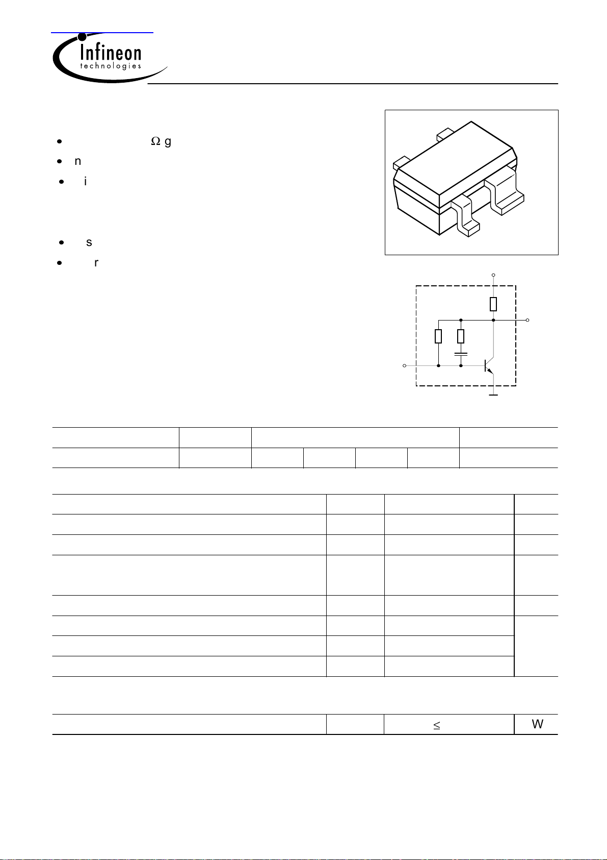
Circuit Diagram
4
3
2
V
D
4
3
2
VPS05605
OUT
EHA07385
1
1
IN
GND
ESD: Electrostatic discharge sensitive device, observe handling precaution!
Type Marking Pin Configuration Package
BGA420 BLs 1, IN 2, GND 3, OUT 4, VD
SOT343
Maximum Ratings
Parameter
Device current
Device voltage
Total power dissipation
Symbol Value Unit
I
V
P
D
D
tot
15 mA
6 V
90 mW
TS = 110 °C
RF input power
Junction temperature
Ambient temperature
Storage temperature
P
T
T
T
RFin
A
st
0 dBm
150 °C
-65 ... 150
-65 ... 150
Thermal Resistance
Junction - soldering point
1
For calculation of R
please refer to Application Note Thermal Resistance
thJA
1)
R
thJS
410
K/W
Jan-29-20021
BGA420
Electrical Characteristics at TA = 25 °C, unless otherwise specified.
Parameter Symbol Values Unit
min. typ. max.
AC characteristics VD = 3 V, Z
Device current
Insertion power gain
f = 0.1 GHz
f = 1 GHz
f = 1.8 GHz
Reverse isolation
f = 1.8 GHz
Noise figure
f = 0.1 GHz
f = 1 GHz
f = 1.8 GHz
Intercept point at the output
f = 1 GHz
1dB compression point
f = 1 GHz
Return loss input
f = 1.8 GHz
Return loss output
f = 1.8 GHz
= 50
o
I
D
|S21|
2
5.4 6.7 8 mA
17
15
11
S12
25 28 -
NF
IP
P
RL
RL
3out
-1dB
in
out
10 13 - dBm
12 16 -
19
17
13
-
-
-
1.9
2.2
2.3
2.3
2.6
2.7
dB
-
-
-
-6 -2.5 -
8 11 - dB
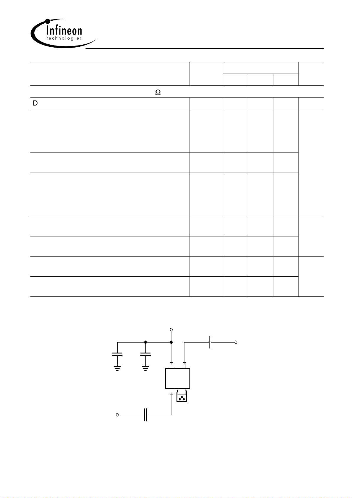
Typical biasing configuration
V
+
D
100 pF
RF OUT
10 nF100 pF
4
3
BGA 420
12
100 pF
RF IN
Note: 1) Large-value capacitors should be connected from pin 4 to ground right at the device
to provide a low impedance path.
2) The use of plated through holes right at pin 2 is essential for pc-board-applications. Thin
boards are recommended to minimize the parasitic inductance to ground.
GND
EHA07386
Jan-29-20022
 Loading...