

Infineon BFS481 Schematic [ru]
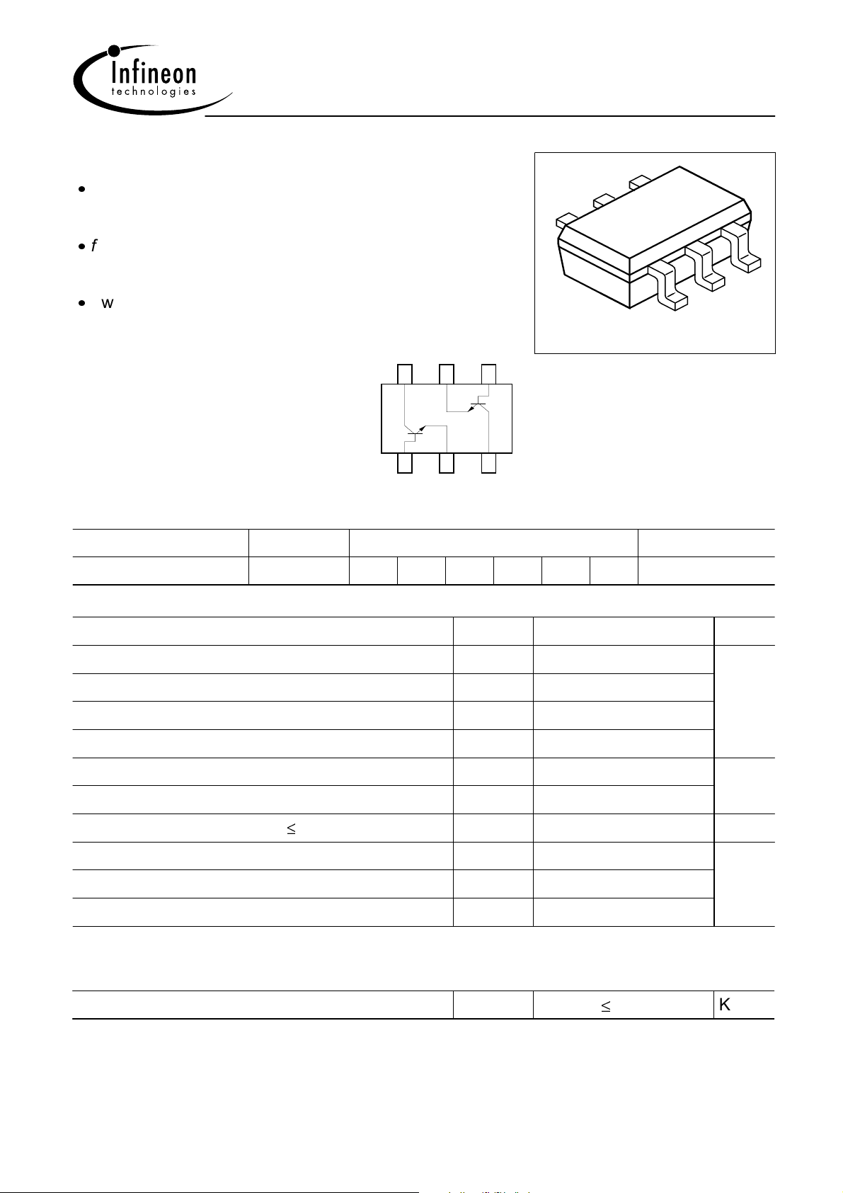
NPN Silicon RF Transistor
g
For low-noise, high-gain broadband amplifier
at collector currents from 0.5 mA to 12 mA
fT = 8 GHz
BFS 481
4
5
6
F = 1.4 dB at 900 MHz
Two (galvanic) internal isolated
Transistors in one package
C1 E2 B2
6 54
TR2
TR1
321
C2E1B1
EHA07196
1
VPS05604
ESD: Electrostatic discharge sensitive device, observe handling precaution!
Type Marking Pin Configuration Package
BFS 481 RFs 1=B 2=E 3=C 4=B 5=E 6=C SOT-363
Maximum Ratings
Parameter
Collector-emitter voltage
Collector-emitter voltage
Collector-base voltage
Emitter-base voltage
Collector current
Base current
Total power dissipation, TS 83 °C
Junction temperature
Ambient temperature
Storage temperature
1)
Symbol Value Unit
V
V
V
V
I
I
P
T
T
T
C
B
CEO
CES
CBO
EBO
tot
j
A
st
12 V
20
20
2
20 mA
2
175 mW
150 °C
-65 ... 150
-65 ... 150
3
2
Thermal Resistance
Junction - soldering point
1
T
is measured on the collector lead at the soldering point to the pcb
S
R
thJS
380
K/W
1 Oct-12-1999
Electrical Characteristics at TA = 25°C, unless otherwise specified.
BFS 481
Parameter
DC characteristics
Collector-emitter breakdown voltage
= 1 mA, IB = 0
I
C
Collector-emitter cutoff current
V
= 20 V, VBE = 0
CE
Collector-base cutoff current
V
= 10 V, IE = 0
CB
Emitter-base cutoff current
= 1 V, IC = 0
V
EB
DC current gain
= 5 mA, VCE = 8 V
I
C
Symbol Values Unit
min. typ. max.
V
(BR)CEO
I
CES
I
CBO
I
EBO
h
FE
12 - - V
- - 100 µA
- - 100 nA
- - 1 µA
50 100 200 -
2 Oct-12-1999
 Loading...