

Page 1
User Guide Please read the Important Notice and Warnings at the end of this document Revision 1.3
www.infineon.com 2020-09-11
Battery Switch 24V - System Demonstrator
User Guide
About this document
Scope and purpose
This Board User Manual provides a short introduction into the Battery Switch 24V - System Demonstrator and
its application.
Intended audience
Electrical engineers who are qualified and familiar with the challenges of handling high current circuits.
Page 2

User Guide 2 Revision 1.3
2020-09-11
Battery Switch 24V - System Demonstrator
User Guide
Important notice
Important notice
The Evaluation Boards and Reference Boards as well as the information in this document are solely intended to
support designers of applications in evaluating the use of products from Infineon Technologies for their
intended applications.
Environmental conditions have been considered in the design of the Evaluation Boards, Reference Boards and
the like provided by Infineon Technologies. The design of the Evaluation Boards and Reference Boards has
been tested by Infineon Technologies only as described in this document. The design is not qualified in terms of
safety requirements, manufacturing and operation over the entire operating temperature range or lifetime.
The Evaluation Boards and Reference Boards provided by Infineon Technologies are subject to functional
testing only under typical load conditions. Evaluation Boards and Reference Boards are not subject to the same
procedures as regular products regarding returned material analysis (RMA), process change notification (PCN)
and product discontinuation (PD).
Evaluation Boards and Reference Boards are not commercialized products, and are solely intended for
evaluation and testing purposes. In particular, they shall not be used for reliability testing or production. The
Evaluation Boards and Reference Boards may therefore not comply with CE or similar standards (including but
not limited to the EMC Directive 2004/EC/108 and the EMC Act) and may not fulfill other requirements of the
country in which they are operated by the customer. The customer shall ensure that all Evaluation Boards and
Reference Boards will be handled in a way which is compliant with the relevant requirements and standards of
the country in which they are operated.
The Evaluation Boards and Reference Boards as well as the information provided in this document are
addressed only to qualified and skilled technical staff, for laboratory usage, and shall be used and managed
according to the terms and conditions set forth in this document and in other related documentation supplied
with the respective Evaluation Board or Reference Board.
It is the responsibility of the customer’s technical departments to evaluate the suitability of the Evaluation
Boards and Reference Boards for the intended application, and to evaluate the completeness and correctness
of the information provided in this document with respect to such application.
The customer accepts that the Evaluation Boards and Reference Boards are not intended to be used in lifeendangering applications such as medical, nuclear, military, life-critical or other applications, where failure
of the Evaluation Boards and Reference Boards, or any results from the use thereof, can reasonably be
expected to result in personal injury.
The Evaluation Boards and Reference Boards and any information in this document is provided "as is" and
Infineon Technologies disclaims any warranties, express or implied, including but not limited to warranties of
non-infringement of third party rights and implied warranties of fitness for any purpose, or for merchantability.
Infineon Technologies shall not be responsible for any damages resulting from the use of the Evaluation Boards
and Reference Boards and/or from any information provided in this document. The customer is obliged to
defend, indemnify and hold Infineon Technologies harmless from and against any claims or damages arising
out of or resulting from any use thereof.
Infineon Technologies reserves the right to modify this document and/or any information provided herein at
any time without further notice.
Page 3

User Guide 3 Revision 1.3
2020-09-11
Battery Switch 24V - System Demonstrator
User Guide
Table of contents
Table of contents
About this document ....................................................................................................................... 1
Important notice ............................................................................................................................ 2
Table of contents ............................................................................................................................ 3
1 Overview ...................................................................................................................... 4
2 Connecting the Switch ................................................................................................... 6
2.1 Overview .................................................................................................................................................. 6
2.2 Control ..................................................................................................................................................... 7
2.2.1 Pin Assignment ................................................................................................................................... 7
2.2.2 Input Voltage Range ........................................................................................................................... 8
2.2.3 Control with bistable relay adaptor .................................................................................................. 9
3 Operating Range ........................................................................................................... 10
3.1 Voltage Range ........................................................................................................................................ 10
3.2 Current Rating ....................................................................................................................................... 10
4 Thermal Behavior ......................................................................................................... 11
5 Switching Behaviour ..................................................................................................... 12
6 Mechanical Dimensions ................................................................................................. 13
7 Schematics .................................................................................................................. 14
8 PCB Description ............................................................................................................ 17
8.1 PCB Technology .................................................................................................................................... 17
8.2 PCB Layout ............................................................................................................................................ 18
9 Bill Of Materials ............................................................................................................ 19
Revision History ............................................................................................................................ 20
Page 4
User Guide 4 Revision 1.3
2020-09-11
Battery Switch 24V - System Demonstrator
User Guide
Overview
1 Overview
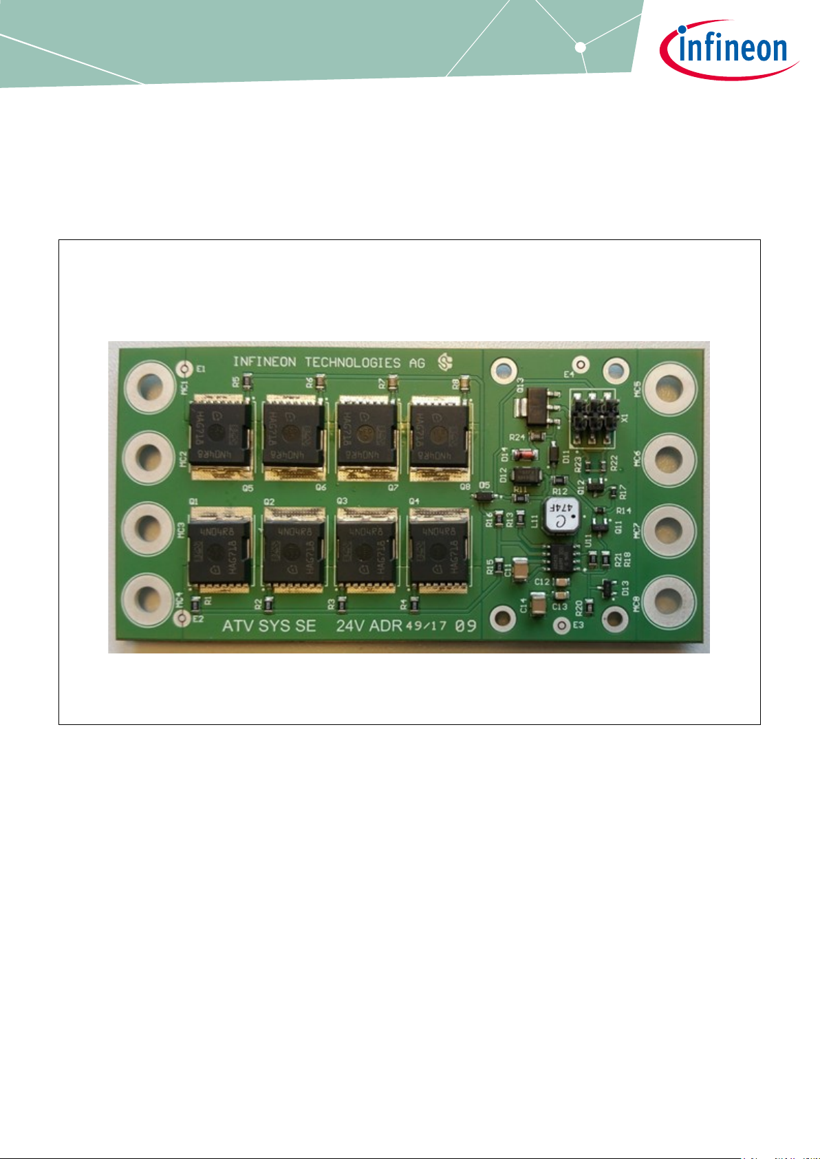
The Battery Switch 24V - System Demonstrator shows a semiconductor based solution of a 24 V battery master
switch for trucks.
Note: This demonstrator focus lies solely on the switching element and the demonstration of the current
carrying and short circuit handling capabilities.
The demonstrator consists of eight low ohmic MOSFETs connected in parallel and mounted on a structured
copper IMS (insolated metal substrate) board together with a gate driver circuit to switch those MOSFETs on
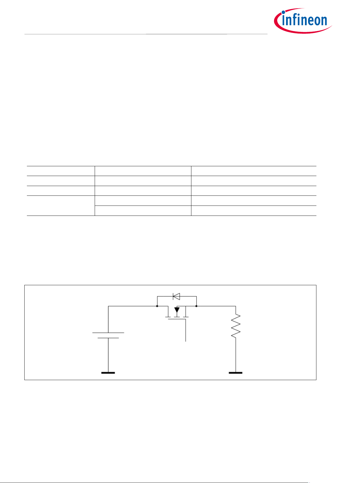
and off. In order to protect the MOSFETs against excessive overvoltage there are four transient voltage
suppressor diodes implemented at the bottom side of the board.
Table 1 Main Components
Component
Type
Comment
MOSFETs (8x)
IPLU300N04S4-R8
300 A, 40 V, 0.53 mOhm typ.
TVS Diodes (4x)
SMDJ33A
33 V
Gate Driver
AUIR3242S
Normally on (default)
AUIR3241S
Normally off (optional)
Thanks to the low ohmic MOSFETs the on state resistance of the whole switch is less than 160 uΩ from terminal
to terminal. The eight parallel MOSFETs account for typically 67 uΩ at room temperature. At 120°C board
temperature and 500 A current this value will increase to roughly 100 uΩ.
Please note that the Battery Switch 24V - System Demonstrator is a unidirectional switch. This means that it will
interrupt current flowing from the battery to the load but not current flowing into the battery. The reason for
this is the intrinsic body diode of the power MOSFETs as shown in Figure 1. Therefore charging through the
MOSFETs should be avoided or at least limited to currents below 20 A when the switch is deactivated (off).
Figure 1 Unidirectional Switch due to MOSFET Body Diode
Page 5
User Guide 5 Revision 1.3
2020-09-11
Battery Switch 24V - System Demonstrator
User Guide
Overview
Figure 2 Battery Switch 24V - System Demonstrator Top View
Figure 3 Battery Switch 24V - System Demonstrator Bottom View
Page 6
User Guide 6 Revision 1.3
2020-09-11
Battery Switch 24V - System Demonstrator
User Guide
Connecting the Switch
2 Connecting the Switch
2.1 Overview
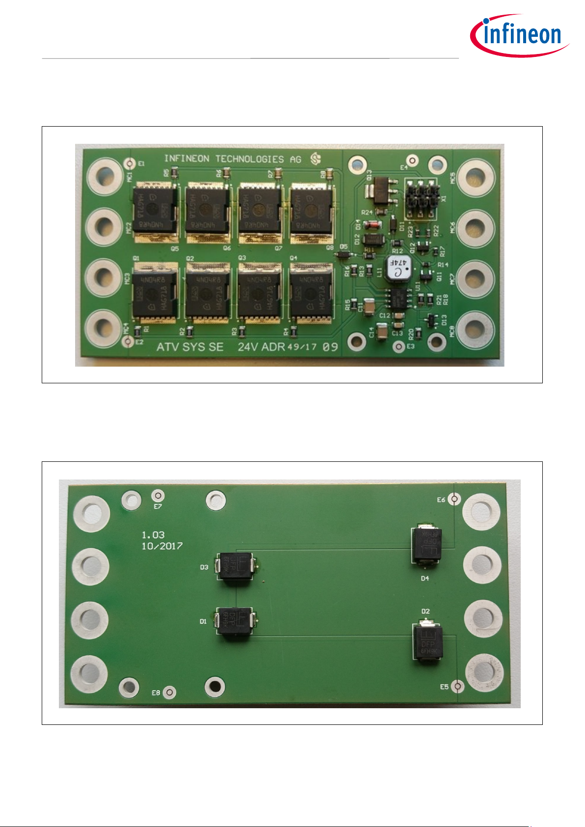
Figure 4 Basic Connection Diagram
Figure 5 Connecting the Bus Bars with M4 Screws
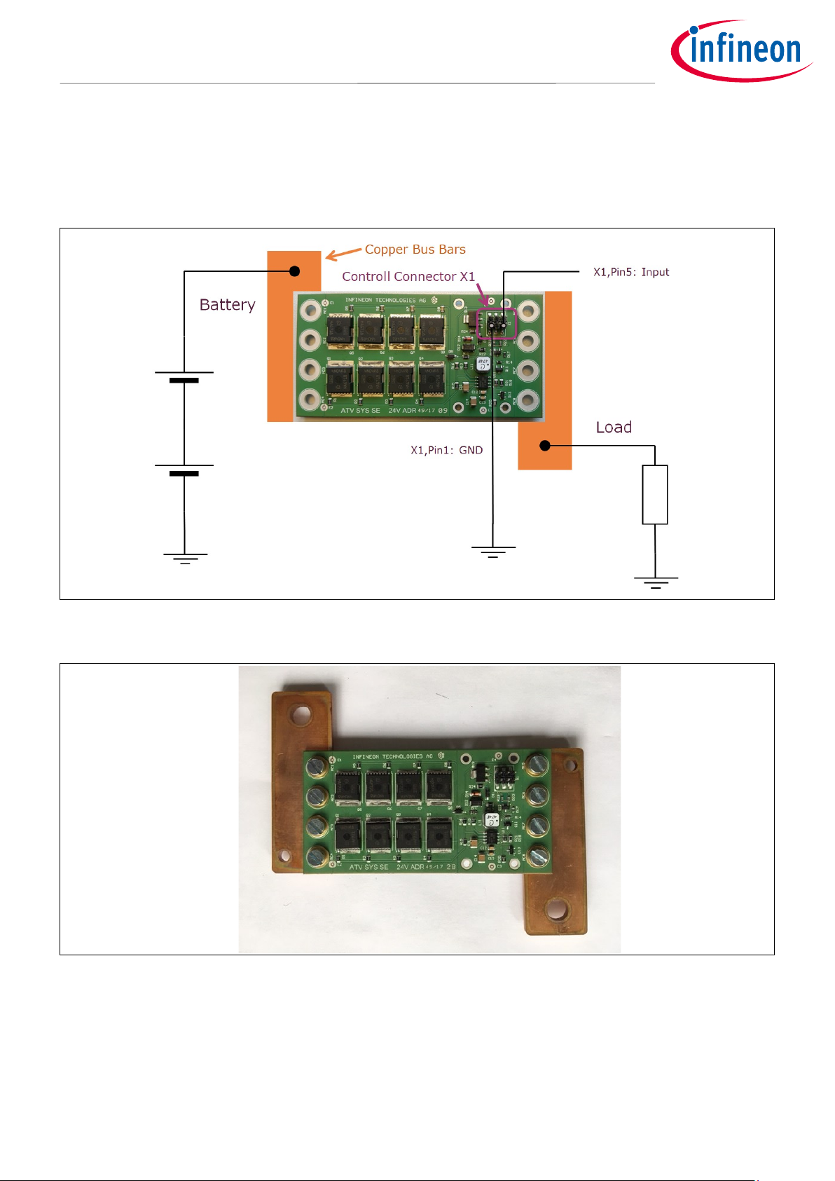
The switch shall be connected between battery and load as pictured in Figure 4. It is recommended to use
copper bus bars to provide a low ohmic current path. To ensure proper contact to the PCB please use copper
washers between the PCB and the bus bar (Figure 6).
Mechanical dimensions of the board and the mounting holes can be found in chapter 6 Mechanical Dimensions
Page 7
User Guide 7 Revision 1.3
2020-09-11
Battery Switch 24V - System Demonstrator
User Guide
Connecting the Switch
Figure 6 Copper washers between PCB and bus bar
2.2 Control
2.2.1 Pin Assignment
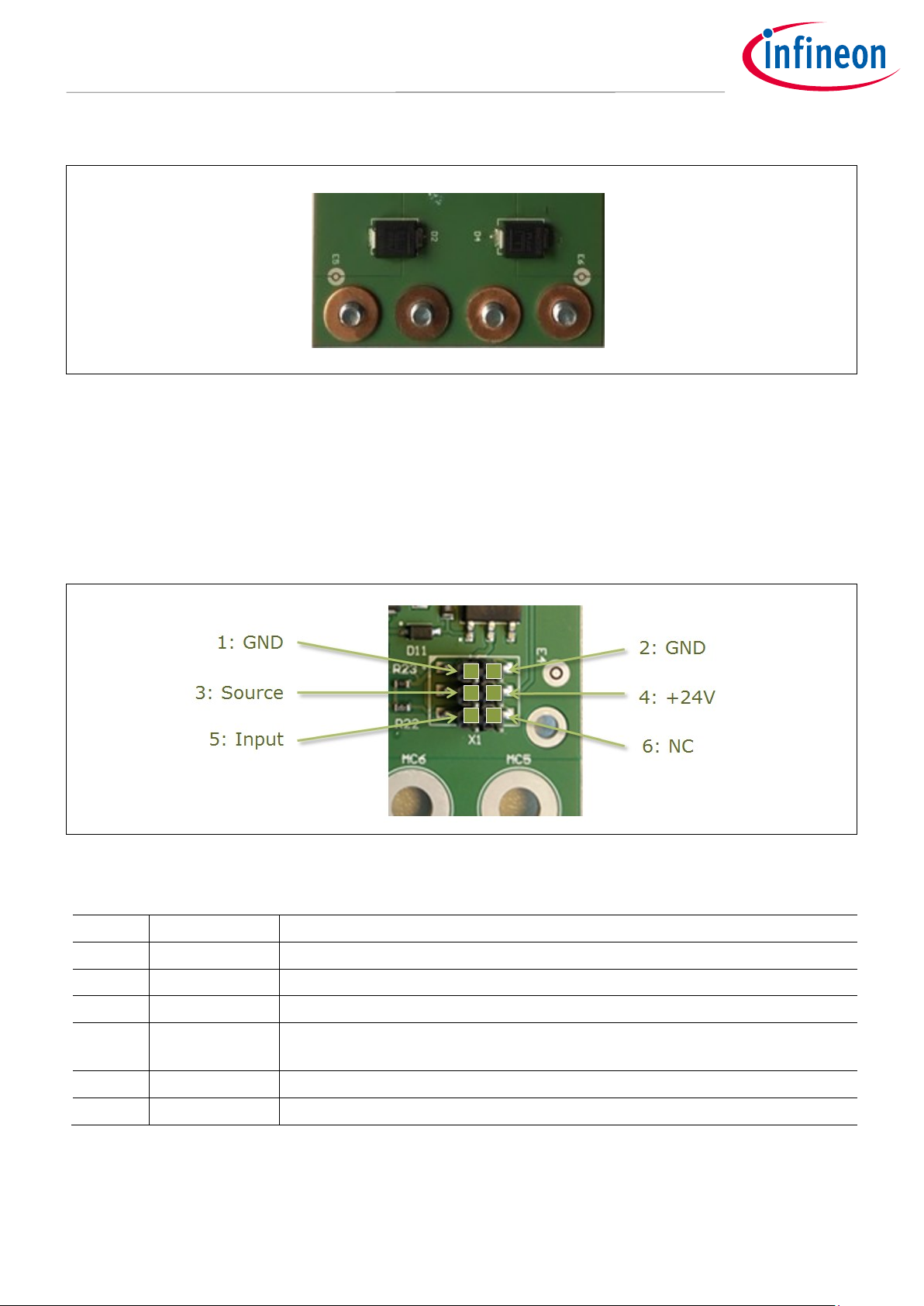
The switch can be controlled by a logic level signal on pin 5 (Input) of the header connector X1.
This connector is a standard 6-pin dual row 2.54 mm header (Samtec TSM-103-01-T-DV).
Figure 7 Controll Connector X1 Pin Assignment
Table 2 X1 Pin Description
Pin
Name
Function
1
GND
Ground
2
GND
Ground
3
Source
Voltage at the output of the switch
4
+24 V
Voltage at the battery terminal of the switch, protected via diode against
reverse polarity. Can be used to power own circuitry3
5
Input
Control signal for switch
6
NC
Not connected
Page 8

User Guide 8 Revision 1.3
2020-09-11
Battery Switch 24V - System Demonstrator
User Guide
Connecting the Switch
2.2.2 Input Voltage Range
The input will accept a very wide input voltage range. Therefore it is possible to drive the switch with 5 V logic
as well as directly from the 24 V battery. The switching threshold is at approximately 0.8 V.
With increasing input voltage the input current will increase. It is mainly determined by the base resistor of the
npn transistor at the input stage (see Figure 8).
Please note that the input should be properly biased by an external pull-down resistor. If the input is left
floating it may react on disturbances like EMC or simply on touching it.
Figure 8 Input Stage
Depending on the driver IC used the switching logic differs. The AUIR3241S is a “normally off” driver, i.e. the
switch is open when the input signal is low and closed when the input signal is high.
For the AUIR3242S the input logic is reversed. That means the switch will be conducting as long as the input
signal is low and be opened when a high signal is applied. The advantage of the “normally on” driver
AUIR3242S is the low quiescent current in “on” condition.
Logic Table
Input Signal
Switch Status for AUIR3242
(default)
Switch Status for AUIR3241
Low
Closed
Open
High
Open
Closed
Page 9

User Guide 9 Revision 1.3
2020-09-11
Battery Switch 24V - System Demonstrator
User Guide
Connecting the Switch
2.2.3 Control with bistable relay adaptor
In order to emulate the behavior of a latching (bistable) power relay the switch can be controlled using an
adptor board with a small bistable relay to drive the input. The adapter board is placed onto the connector X1
as shown in Figure 9.
Figure 9 Mounting of bi-stable relay adaptor board
Figure 10 Schematics of adaptor board
Page 10

User Guide 10 Revision 1.3
2020-09-11
Battery Switch 24V - System Demonstrator
User Guide
Operating Range
3 Operating Range
3.1 Voltage Range
Figure 11 shows the different operating ranges of the switch. The nominal operating voltage range is from 16 V
to 36V.
Figure 11 Operating Voltage Range
3.2 Current Rating
The switch is designed to handle peak currents up to 1800 A. However, due to the on-state resistance of the
switch (160 uΩ typ. at 120°C) high currents will lead to significant power dissipation and a temperature increase
in the MOSFETs. These can handle a maximum junction temperature of 175 °C. Therefore the maximum
allowable duration for high currents is limited depending on the cooling conditions. The values in Table 3 are
estimated for the board exposed to a small air flow of approximately 50 cm / min. and a start temperature of 25
°C.
Table 3 Current Carrying Capability Estimation
Current
Power Dissipation
Duration
300 A
~ 15 W
Continuous
500 A
~ 40 W
~ 10 min.
700 A
~ 80 W
~ 5 min.
1500 A
~ 360 W
~ 15 s
1800 A
~ 520 W
~ 10 s
Page 11

User Guide 11 Revision 1.3
2020-09-11
Battery Switch 24V - System Demonstrator
User Guide
Thermal Behavior
4 Thermal Behavior
Figure 12 Temperature increase at high currents
Even if the on state resistance of the MOSFETs is very small, high currents will lead to power dissipation and
therefore to a temperature increase. The maximum permissible junction temperature of the MOSFETs is 175 °C.
Depending on the cooling conditions there is a limit on how long the switch can withstand the current. Figure
12 shows the temperature curve for a current of 500 A at room temperature and very light airflow around the
board.
Page 12

User Guide 12 Revision 1.3
2020-09-11
Battery Switch 24V - System Demonstrator
User Guide
Switching Behaviour
5 Switching Behaviour
In contrast to relays MOSFETs are switching much faster and cleaner. There is no bouncing of contacts and no
arcing. Switching just takes microseconds instead of several milliseconds. The following oscilloscope pictures
show the switching behavior of the Battery Switch 24V - System Demonstrator with the “normally on”
AUIR3242S driver. Please note that the magenta curve shows the drain source voltage across the MOSFETs, so a
small voltage means the switch is on (conducting) and a high voltage means the switch is off (blocking). The
delay between the input signal and the output is caused by the input circuitry.
Figure 13 Switch Timing – On and Off
In the oscilloscope plots it can be seen that after switching off V_DS reaches 40 V. The reason for this is the load
inductance. When the current flow is interrupted it induces a voltage that pulls the output below ground
potential. As a result V_DS rises. When V_DS reaches the threshold of the transient voltage suppressor (TVS)
diodes these start to conduct and to dissipate a part of the energy stored in the inductance. Another part of the
energy will be taken over by the MOSFETs due to the avalanche effect, which sets in at a V_DS of about 40 V.
Note: The amount of switching energy that can be dissipated by the TVS diodes and the MOSFETs is
limited. In our lab the Battery Switch 24V - System Demonstrator has been tested successfully with
cable inductances of up to 12 µH and currents up to 1600 A. The switch survived energies up to 20
Joule. However, this can just be seen as an indicator but not as a guarantee of which performance
to expect. Since the load inductance is dependent on the specific system setup like cable length, diameter, -routing etc. the suitability of the switch has to be verified for each setup separately.
Page 13

User Guide 13 Revision 1.3
2020-09-11
Battery Switch 24V - System Demonstrator
User Guide
Mechanical Dimensions
6 Mechanical Dimensions
Figure 14 Board Dimensions [mm]
Figure 15 Side View
Page 14

User Guide 14 Revision 1.3
2020-09-11
Battery Switch 24V - System Demonstrator
User Guide
Schematics
7 Schematics
Figure 16 Top Level Schematics
Page 15

User Guide 15 Revision 1.3
2020-09-11
Battery Switch 24V - System Demonstrator
User Guide
Schematics
Figure 17 MOSFET Driver Circuit
Page 16

User Guide 16 Revision 1.3
2020-09-11
Battery Switch 24V - System Demonstrator
User Guide
Schematics
Figure 18 Power Stage
Page 17

User Guide 17 Revision 1.3
2020-09-11
Battery Switch 24V - System Demonstrator
User Guide
PCB Description
8 PCB Description
8.1 PCB Technology
The Printed Circuit Board used for the shown Battery Switch 24V - System Demonstrator is a product idea of
Schweizer Electronic AG. The deployment of the Inlay Board 2.0 technology assures highest current carrying
capability in conjunction with lowest thermal resistance. A superior thermal connection between the MOSFETs
and the integrated power rail of the PCB allows to conduct a permanent current of up to 500 A and a shortcircuit current of up to 1800 A.
Table 4 Feature Set of Metal Core Board (Non-Isolated Version)
Feature
Value
Size
100.0 mm x 50.0 mm
Thickness
1,3 mm
Electrical resistance
60 µΩ
Thermal resistance (non-isolated version)
0.1 K/W
Thermal resistance (isolated version)
~ 0.2 K/W
No. of copper-filled laser vias per MOSFET
300
Figure 19 PCB Stackup
The core of the PCB is a copper plate of 1.0 mm thickness which represents the power rail for the switch. This
copper plate is structured by an isolation gap of 500 µm width. By means of a lamination process the isolation
gap is filled with the resin from Prepreg material. This represents a safe isolation space between battery and
load potential. The outer layers are consisting of 35 µm copper foils, after plating 70 µm. To ensure both a lowohmic electrical connection from the MOSFETs to the current rail and a good heat flow to a potentially used
heatsink, the PCB is provided with hundreds of copper-filled microvias in the soldering area of the MOSFET and
on the back-side of the PCB. The high filling factor with dimple depths lower than 25µm allows the designer to
have the MOSFETs soldered on top of the via field without facing the risk of solder voids. During assembly it has
to be made sure that solder profiles will be used which are appropriate for power PCBs with a large thermal
mass. The MOSFETs are placed on the PCB so that the MOSFETs, once they are turned on, connect the two
isolated parts of the PCB.
Figure 20 Cross Section
Page 18

User Guide 18 Revision 1.3
2020-09-11
Battery Switch 24V - System Demonstrator
User Guide
PCB Description
For higher logic content requirements compared to the presented switch demonstrator the Inlay Board 2.0
technology can optionally accommodate an area with four or more electrical layers next to the power rails.
8.2 PCB Layout
Figure 21 Top Layer
Figure 22 Middle Layer (1mm Cu)
Figure 23 Bottom Layer
Page 19

User Guide 19 Revision 1.3
2020-09-11
Battery Switch 24V - System Demonstrator
User Guide
Bill Of Materials
9 Bill Of Materials
Table 5 BOM
Designator
Value
Description
D1, D2, D3, D4
SMDJ33A
Transient Voltage Suppression Diode, Uni-directional, 33V
D11
MMSZ5256BT1G
Zener Voltage Regulator, 500mW, 30V
D12
SZ1SMA5938BT3
Zener Voltage Regulator, 36V
D13
BZX84C5V1LTG
Zener Voltage Regulator, 5.1V
D14
LL4148
Small Signal Diode, 100V
D5
1N4148W-13-F
Surface Mount Fast Switching Diode
R13
1R
1R/150V/1%
C11, C14
1u/100V
Cap-1210-1u/100V/0.1/X7R
R15, R16
2.2R
2.2R/150V/1%
R14, R23
3.3k
3.3k/75V/1%
R11
5.6R
5.6R/150V/1%
R20
6.8k
6.8k/150V/1%
R22
6.8k
6.8k/75V/1%
R1 .. R8
8.2R
8.2R/150V/1%
R24
10k
10k/150V/1%
R18
12k
12k/150V/1%
R21
12R
12R/150V/1%
R17
22k
22k/75V/1%
C12
100n
Cap-0805-100n/100V/0.1/X7R
R12
100R
100R/150V/1%
C13
220n
Cap-0805-220n/50V/0.1/X7R
L11
470uH
Shielded Power Inductor
U11
AUIR3242S
Low Quiescent Current Back to Back MOSFET Driver
Q13
FZT753
100V PNP High Performance Transistor
Q1 .. Q8
IPLU300N04S4-R8
OptiMOS T2 N-Channel Enhancement Power-Transistor, 40 V
Q11
NSV1C200L
100V, 2.0 A, Low VCEsat PNP Transistor
Q12
NSV1C201L
100V, 3.0 A, Low VCEsat NPN Transistor
X1
TSM-103-01-T-DV
SMT .025" SQ Post Header, 2.54mm, 6 pin, vertical, double row
Page 20

User Guide 20 Revision 1.3
2020-09-11
Battery Switch 24V - System Demonstrator
User Guide
Revision History
Revision History
Major changes since the last revision
Page or Reference
Description of change
Figure 19
New picture
New Filename; new naming
Page 21

Trademarks of Infineon Technologies AG
µHVIC™, µIPM™, µPFC™, AU-ConvertIR™, AURIX™, C166™, CanPAK™, CIPOS™, CIPURSE™, CoolDP™, CoolGaN™, COOLiR™, CoolMOS™, CoolSET™, CoolSiC™,
DAVE™, DI-POL™, DirectFET™, DrBlade™, EasyPIM™, EconoBRIDGE™, EconoDUAL™, EconoPACK™, EconoPIM™, EiceDRIVER™, eupec™, FCOS™, GaNpowIR™,
HEXFET™, HITFET™, HybridPACK™, iMOTION™, IRAM™, ISOFACE™, IsoPACK™, LEDrivIR™, LITIX™, MIPAQ™, ModSTACK™, my-d™, NovalithIC™, OPTIGA™,
OptiMOS™, ORIGA™, PowIRaudio™, PowIRStage™, PrimePACK™, PrimeSTACK™, PROFET™, PRO-SIL™, RASIC™, REAL3™, SmartLEWIS™, SOLID FLASH™,
SPOC™, StrongIRFET™, SupIRBuck™, TEMPFET™, TRENCHSTOP™, TriCore™, UHVIC™, XHP™, XMC™
Trademarks updated November 2015
Other Trademarks
All referenced product or service names and trademarks are the property of their respective owners.
Edition 2020-09-11
Published by
Infineon Technologies AG
81726 Munich, Germany
© 2020 Infineon Technologies AG.
All Rights Reserved.
IMPORTANT NOTICE
The information contained in this application note is
given as a hint for the implementation of the product
only and shall in no event be regarded as a
description or warranty of a certain functionality,
condition or quality of the product. Before
implementation of the product, the recipient of this
application note must verify any function and other
technical information given herein in the real
application. Infineon Technologies hereby disclaims
any and all warranties and liabilities of any kind
(including without limitation warranties of noninfringement of intellectual property rights of any
third party) with respect to any and all information
given in this application note.
The data contained in this document is exclusively
intended for technically trained staff. It is the
responsibility of customer’s technical departments
to evaluate the suitability of the product for the
intended application and the completeness of the
product information given in this document with
respect to such application.
For further information on the product, technology,
delivery terms and conditions and prices please
contact your nearest Infineon Technologies office
(www.infineon.com).
WARNINGS
Due to technical requirements products may contain
dangerous substances. For information on the types
in question please contact your nearest Infineon
Technologies office.
Except as otherwise explicitly approved by Infineon
Technologies in a written document signed by
authorized representatives of Infineon
Technologies, Infineon Technologies’ products may
not be used in any applications where a failure of the
product or any consequences of the use thereof can
reasonably be expected to result in personal injury.
 Loading...