

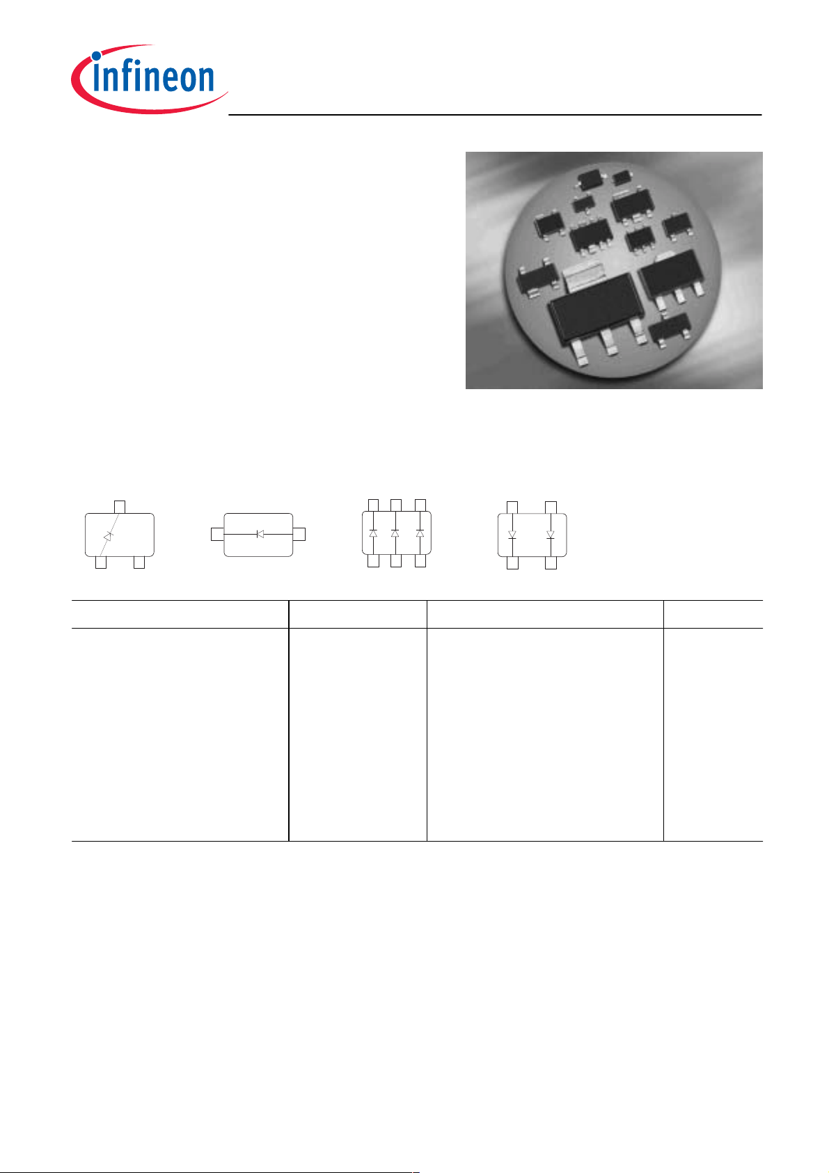
Silicon Switching Diode
• For high-speed switching applications
BAS16...
BAS16
BAS16W
BAS16-02L
BAS16-02V
BAS16U
BAS16-07L4BAS16S
BAS16-02W
BAS16-03W
"
!
#$
,
, , !
!
!"
,
,
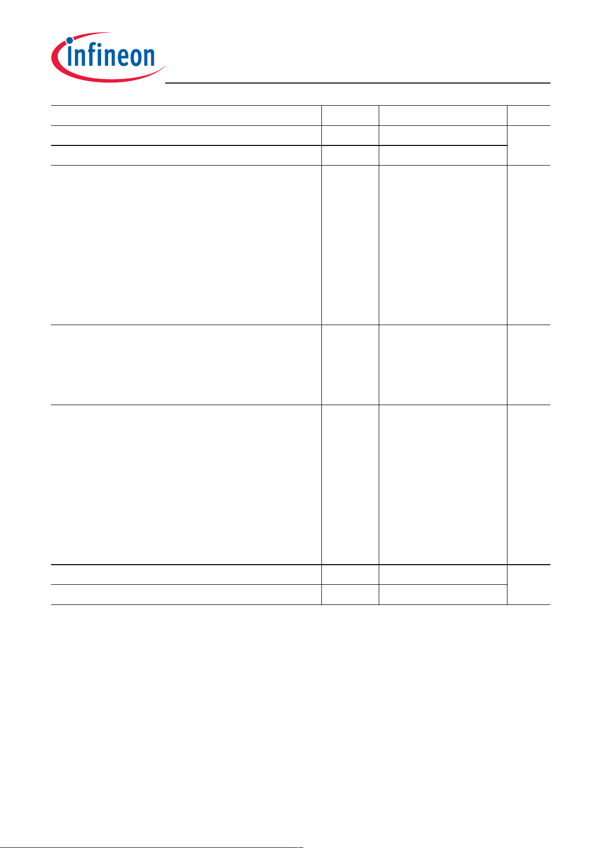
Type Package Configuration Marking
BAS16
BAS16-02L*
BAS16-02V
BAS16-02W
BAS16-03W
BAS16-07L4*
BAS16S
BAS16U
SOT23
TSLP-2-1
SC79
SCD80
SOD323
TSLP-4-4
SOT363
SC74
single
single, leadless
single
single
single
parallel pair, leadless
parallel triple
parallel triple
A6s
A6
6
A6
B
6A
A6s
A6s
BAS16W
* Preliminary Data
SOT323
single
1
A6s
2005-11-08
Maximum Ratings at TA = 25°C, unless otherwise specified
g
BAS16...
Parameter
Diode reverse voltage V
Peak reverse voltage V
Forward current
BAS16
BAS16-02L, -07L4
BAS16-02V, -02W
BAS16-03W
BAS16S
BAS16U
BAS16W
Non-repetitive peak surge forward current
t = 1 µs, BAS16/ S/ U/ W/ -03W
t = 1 µs, BAS16-02L/ -02V/ -02W/ -07L4
t = 1 s
Symbol Value Unit
R
RM
I
F
80 V
85
mA
250
200
200
250
200
200
250
I
FSM
A
4.5
2.5
0.5
Total power dissipation
BAS16, T
BAS16-02L, -07L4, T
BAS16-02V, -02W, T
BAS16-03W, T
BAS16S, T
BAS16U, T
BAS16W, T
≤ 54 °C
S
S
≤ 85 °C
S
≤ 113 °C
S
≤ 119 °C
S
≤ 130 °C
S
≤ 120 °C
S
≤ 116 °C
Junction temperature T
Storage temperature T
P
tot
j
st
370
250
250
250
250
250
250
150 °C
-65 ... 150
mW
2
2005-11-08
Thermal Resistance
BAS16...
Parameter
Junction - soldering point1)
Symbol Value Unit
R
thJS
BAS16, BAS16S
BAS16-02L, -07L4
BAS16-02V, -02W
BAS16-03W
BAS16U
BAS16W
Electrical Characteristics at TA = 25°C, unless otherwise specified
Parameter
Symbol Values Unit
min. typ. max.
DC Characteristics
Breakdown voltage
I
= 100 µA
(BR)
Reverse current
V
= 75 V
R
V
= 25 V, TA = 150 °C
R
V
= 75 V, TA = 150 °C
R
V
I
R
(BR)
85 - - V
-
-
-
≤ 260
≤ 80
≤ 120
≤ 135
≤ 150
≤ 125
-
-
-
0.1
30
50
K/W
µA
Forward voltage
I
= 1 mA
F
I
= 10 mA
F
I
= 50 mA
F
I
= 100 mA
F
I
= 150 mA
F
Forward recovery voltage
I
= 10 mA, tP = 20 ns
F
1
For calculation of R
please refer to Application Note Thermal Resistance
thJA
V
V
F
-
-
-
-
-
fr
- - 1.75 V
-
-
-
-
-
715
855
1000
1200
1250
mV
3
2005-11-08
Electrical Characteristics at TA = 25°C, unless otherwise specified
Parameter
Symbol Values Unit
min. typ. max.
AC Characteristics
BAS16...
Diode capacitance
V
= 0 V, f = 1 MHz
R
Reverse recovery time
I
= 10 mA, IR = 10 mA, measured at IR = 1mA ,
F
R
= 100 Ω
L
C
t
T
rr
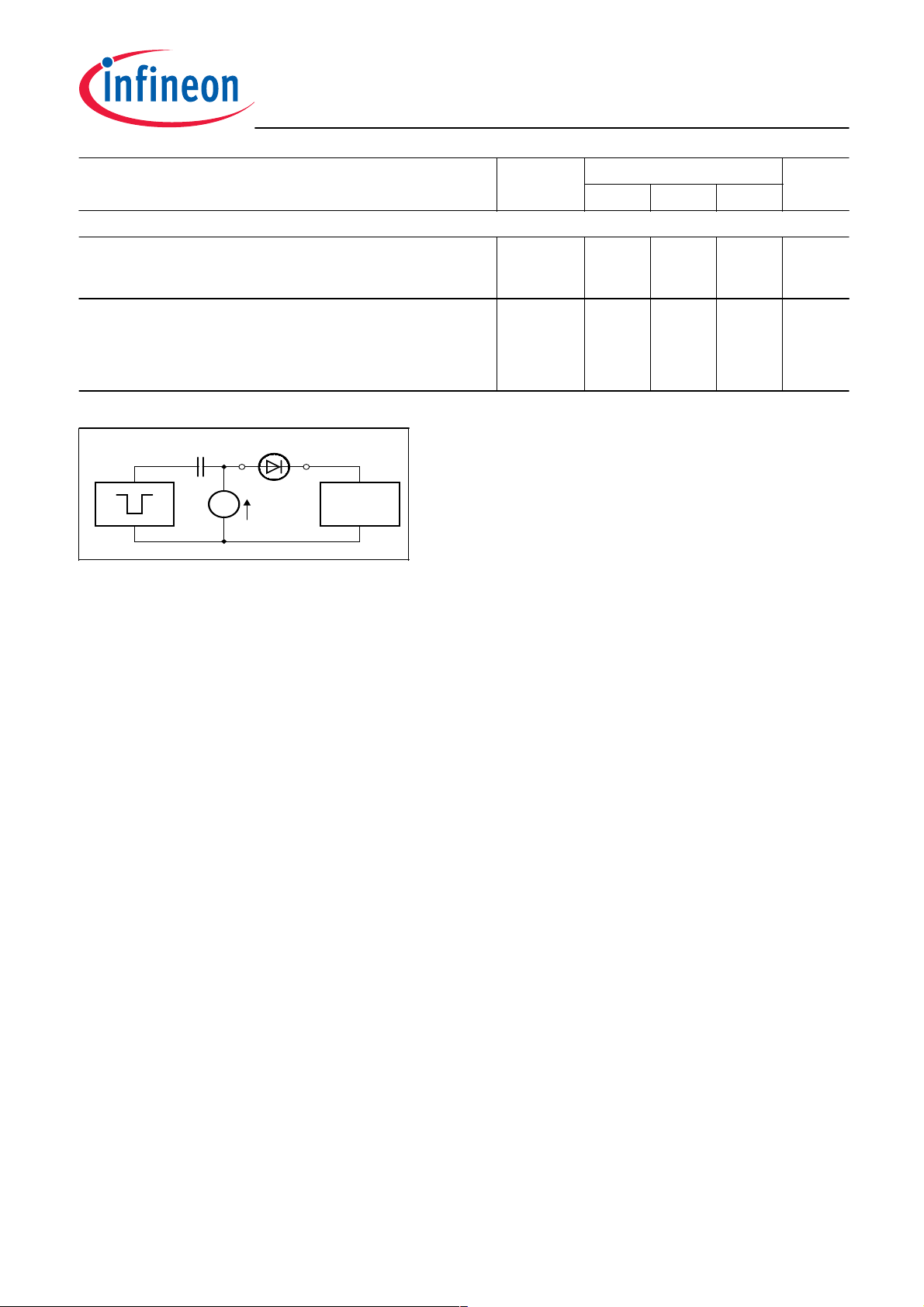
Test circuit for reverse recovery time
D.U.T.
Pulse generator: tp = 100ns, D = 0.05, tr = 0.6ns,
R
Ι
F
Oscillograph
Oscillograph: R = 50Ω, t
EHN00017
- - 2 pF
- - 4 ns
= 50Ω
i
= 0.35ns, C = 0.05pF
r
4
2005-11-08
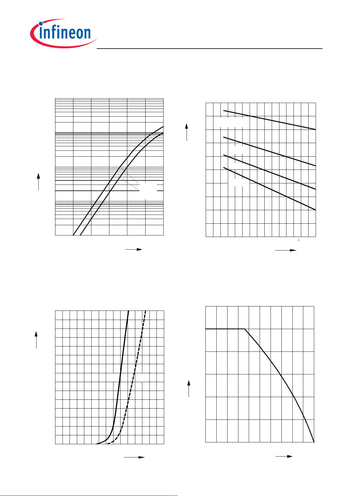
BAS16...
Reverse current IR = ƒ (TA)
V
= Parameter
R
5
10
nA
4
10
R
I
3
10
2
10
1
10
0 25 50 75 100
70 V
25 V
°C
Forward Voltage VF = ƒ (TA)
I
= Parameter
F
BAS 16 EHB00025
1.0
V
V
F
0.5
150
T
A
Ι
= 100 mA
F
10 mA
1 mA
0.1 mA
0
0 50 100 150
C
T
A
Forward current IF = ƒ (VF)
T
= 25°C
A
150
Ι
F
mA
100
50
0
0
0.5 1.0 V 1.5
Forward current IF = ƒ (TS)
BAS16
EHB00023BAS 16
maxtyp
V
F
300
mA
200
F
I
150
100
50
0
0 15 30 45 60 75 90 105 120
°C
150
T
S
5
2005-11-08
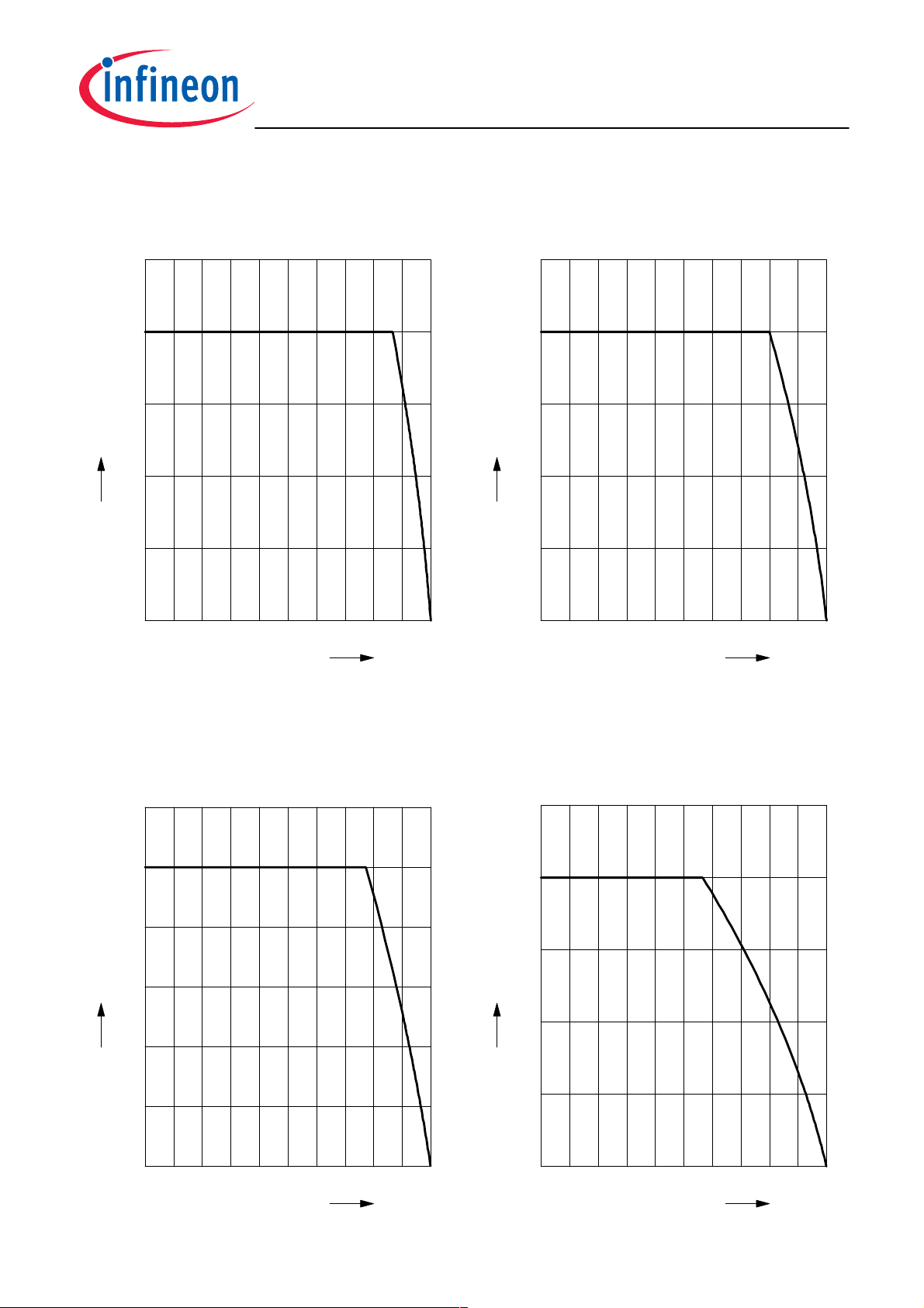
BAS16...
Forward current IF = ƒ (TS)
BAS16-02L, -07L4
250
mA
F
I
150
100
50
0
0 15 30 45 60 75 90 105 120
°C
Forward current IF = ƒ (TS)
BAS16-02V, -02W
250
mA
F
I
150
100
50
150
T
S
0
0 15 30 45 60 75 90 105 120
°C
150
T
S
Forward current IF = ƒ (TS)
BAS16-03W
300
mA
200
F
I
150
100
50
0
0 15 30 45 60 75 90 105 120
°C
Forward current IF = ƒ (TS)
BAS16S
250
mA
F
I
150
100
50
150
T
S
0
0 15 30 45 60 75 90 105 120
°C
T
150
S
6
2005-11-08
BAS16...
Forward current IF = ƒ (TS)
BAS16U
250
mA
200
175
F
I
150
125
100
75
50
25
0
0 15 30 45 60 75 90 105 120
T
°C
Forward current IF = ƒ (TS)
BAS16W
300
mA
200
F
I
150
100
50
150
0
0 15 30 45 60 75 90 105 120
S
°C
150
T
S
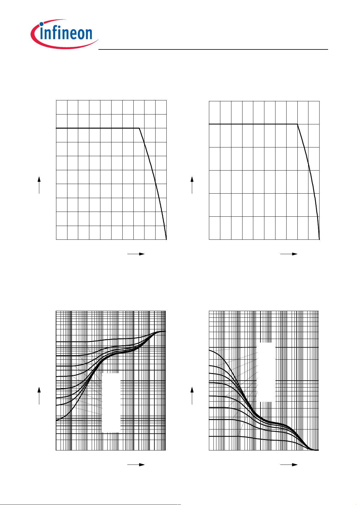
Permissible Puls Load R
BAS16
3
10
K/W
2
10
thJS
R
10
10
10
-1
1
0
10
-7
-6
10
10
0.5
0.2
0.1
0.05
0.02
0.01
0.005
D = 0
-5
-4
10
thJS
10
= ƒ (tp)
-3
10
Permissible Pulse Load
I
Fmax
/ I
FDC
= ƒ (tp)
BAS16
2
10
FDC
/I
Fmax
I
1
10
0
-2
s
t
0
10
p
10
10
-7
-6
10
10
D = 0
0.005
0.01
0.02
0.05
0.1
0.2
0.5
-5
-4
-3
10
10
10
-2
t
0
s
10
p
7
2005-11-08

BAS16...
Permissible Puls Load R
BAS16-02L, -07L4
2
10
K/W
thJS
R
10
0.5
0.2
0.1
0.05
0.02
0.01
0.005
D = 0
-4
-3
10
10
10
1
0
10
-6
-5
10
thJS
10
= ƒ (tp)
-2
10
Permissible Pulse Load
I
Fmax
/ I
FDC
= ƒ (tp)
BAS16-02L, -07L4
2
10
-
FDC
/ I
10
D = 0
0.005
0.01
0.02
0.05
0.1
0.2
0.5
-4
10
-3
10
-2
s
t
0
10
p
Fmax
I
1
10
0
-1
1
s
10
t
p
10
10
-6
10
-5
Permissible Puls Load R
BAS16-02V, -02W
3
10
K / W
2
10
thJS
R
1
10
0
10
-6
10
10
-5
10
-4
10
thJS
-3
= ƒ (tp)
D=0.5
0.2
0.1
0.05
0.02
0.01
0.005
0
-2
10
Permissible Pulse Load
I
Fmax
/ I
FDC
= ƒ (tp)
BAS16-02V, -02W
2
10
10
-4
D=0
0.005
0.01
0.02
0.05
0.1
0.2
0.5
10
-3
10
-2
s
t
0
10
p
FDC
/ I
Fmax
I
1
10
0
10
s
t
0
10
p
10
-6
10
-5
8
2005-11-08

BAS16...
Permissible Puls Load R
BAS16-03W
3
10
K/W
2
10
thJS
R
1
10
0
10
-6
10
10
-5
10
-4
10
thJS
D=0.5
0.2
0.1
0.05
0.02
0.01
0.005
0
-3
= ƒ (tp)
-2
10
Permissible Pulse Load
I
Fmax
/ I
FDC
= ƒ (tp)
BAS16-03W
2
10
10
D=0
0.005
0.01
0.02
0.05
0.1
0.2
0.5
-3
10
-2
s
t
0
10
p
FDC
/ I
Fmax
I
1
10
0
s
t
0
10
p
10
10
-6
10
-5
-4
10
Permissible Puls Load R
BAS16S
3
10
K/W
2
10
thJS
R
1
10
0
10
-6
10
10
-5
10
-4
10
thJS
D=0.5
0.2
0.1
0.05
0.02
0.01
0.005
0
-3
= ƒ (tp)
-2
10
Permissible Pulse Load
I
Fmax
/ I
FDC
= ƒ (tp)
BAS16S
2
10
-
FDC
/ I
Fmax
I
1
10
0
s
t
0
10
p
10
10
-6
10
-5
-4
10
10
D = 0
0.005
0.01
0.02
0.05
0.1
0.2
0.5
-3
10
-2
s
t
0
10
p
9
2005-11-08

BAS16...
Permissible Puls Load R
BAS16U
3
10
K/W
2
10
thJS
R
1
10
0
10
-6
10
10
-5
10
-4
10
thJS
D=0.5
0.2
0.1
0.05
0.02
0.01
0.005
0
-3
= ƒ (tp)
-2
10
Permissible Pulse Load
I
Fmax
/ I
FDC
= ƒ (tp)
BAS16U
2
10
FDC
/ I
Fmax
I
1
10
0
s
t
0
10
p
10
10
-6
10
-5
10
D=0
0.005
0.01
0.02
0.05
0.1
0.2
0.5
-4
10
-3
10
-2
s
t
0
10
p
Permissible Puls Load R
BAS16W
3
10
K/W
2
10
thJS
R
1
10
0
10
-6
10
10
-5
10
-4
10
thJS
0.5
0.2
0.1
0.05
0.02
0.01
0.005
D = 0
-3
= ƒ (tp)
-2
10
Permissible Pulse Load
I
Fmax
/ I
FDC
= ƒ (tp)
BAS16W
2
10
-
FDC
/ I
Fmax
I
1
10
0
s
t
0
10
p
10
10
-6
10
-5
-4
10
10
D = 0
0.005
0.01
0.02
0.05
0.1
0.2
0.5
-3
10
-2
s
t
0
10
p
10
2005-11-08

Package Outline
Foot Print
Pin 1
marking
±0.2
2.9
(2.25)
1.9
Package SC74
B
(0.35)
546
321
+0.1
0.35
-0.05
0.95
0.2
M
0.5
BAS16...
1.1 MAX.
+0.1
0.15
-0.06
±0.1
±0.1
2.5
0.25
6x
B
10˚ MAX.
0.1 MAX.
M
A0.2
±0.1
1.6
10˚ MAX.
A
Marking Layout
Laser
marking
Standard Packing
Reel ø180 mm = 3.000 Pieces/Reel
Reel ø330 mm = 10.000 Pieces/Reel
1.9
0.95
Manufacturer
Date code (Year/Month)
Type code
2.9
Pin 1
marking
2005, June
BCW66H
Example
Pin 1
marking
4
3.15
2.7
11
0.2
8
1.15
2005-11-08

Package Outline
Foot Print
Package SC79
±0.1
0.8
2
Cathode
marking
1
0.3
±0.05
±0.1
1.6
0.55
MAX.
˚
10
±0.04
M
A0.2
0.13
+0.05
-0.03
A
MAX.
˚
10
±0.1
1.2
±0.05
0.2
BAS16...
Marking Layout
Standard Packing
Reel ø180 mm = 3.000 Pieces/Reel
Reel ø330 mm = 10.000 Pieces/Reel
1.35
Date code
Type code
Laser marking
0.35
0.35
2003, July
BAR63-02V
Cathode marking
Example
Cathode
marking
4
1.96
1.33
8
0.4
0.93
12
0.2
0.66
2005-11-08

Package Outline
Foot Print
Cathode
marking
Package SCD80
0.2MA
±0.1
0.8
2
MAX.
˚
±0.1
10
1.7
1
±0.05
0.3
0.7
0.13
±0.1
+0.05
-0.03
˚
±1.5
˚
7
BAS16...
A
±0.1
1.3
±0.05
0.2
Marking Layout
Standard Packing
Reel ø180 mm = 3.000 Pieces/Reel
Reel ø330 mm = 10.000 Pieces/Reel
1.45
Date code
Type code
Laser marking
0.35
0.35
2003, July
BAR63-02W
Cathode marking
Example
Cathode
marking
4
1.45
8
2.5
0.4
0.9
13
0.2
0.7
2005-11-08

BAS16...
Data Code marking for discrete packages with
one digit (SCD80, SC79) CES-Code
Month 2003 2004 2005 2006 2007 2008 2009 2010 2011 2012 2013 2014
01apAPapAPapAP
02bqBQbqBQbqBQ
03crCRcrCRcrCR
04 d s D S d s D S d s D S
05etETetETetET
06fuFUfuFUfuFU
07gvGVgvGVgvGV
08hxHXhxHXhxHX
09j yJYj yJYj y JY
10kzKZkzKZkzKZ
11l 2L4 l 2L4 l 2L4
12n3N5n3N5n3N5
62
14
2005-11-08

Package Outline
Foot Print
Package SOD323
+0.2
1.25
-0.1
2
1
0.3
+0.1
-0.05
M
A
Cathode
marking
±0.2
2.5
0.25
0
±0.05
±0.15
0.45
0.9
+0.2
-0.1
0.15
+0.2
0.3
+0.1
-0.06
A
-0.1
1.7
+0.05
-0.2
BAS16...
Marking Layout
Standard Packing
Type code
Laser marking
0.80.8
1.7
0.6
BAR63-03W
Cathode marking
Example
Reel ø180 mm = 3.000 Pieces/Reel
Reel ø330 mm = 10.000 Pieces/Reel
Cathode
marking
4
8
2
2.9
0.65
0.2
1
1.35
15
2005-11-08

Package Outline
Foot Print
Package SOT23
±0.1
2.9
12
1)
+0.1
0.4
-0.05
1.9
0.25MBC
1) Lead width can be 0.6 max. in dambar area
B
3
C
0.95
0.8
0.15 MIN.
±0.15
2.4
0.2
±0.1
1
0.1 MAX.
10˚ MAX.
0.08...0.15
0...8˚
M
A
±0.1
1.3
10˚ MAX.
A
BAS16...
Marking Layout
12
Pin 1
s
Standard Packing
Reel ø180 mm = 3.000 Pieces/Reel
Reel ø330 mm = 10.000 Pieces/Reel
0.8 1.2
Manufacturer
Date code (Year/Month)
Type code
4
0.9
0.9 0.91.3
EH
Example
0.2
s
2003, July
37
BCW66
Pin 1
3.15
2.13
16
2.65
8
1.15
2005-11-08

Package Outline
Package SOT323
±0.2
2
0.3
+0.1
-0.05
3x
M
0.1
3
0.1 MAX.
0.1
0.9
BAS16...
±0.1
A
Foot Print
Marking Layout
12
0.650.65
0.6
1.6
0.8
0.65
0.65
±0.1
2.1
0.1 MIN.
M
0.2 A
0.15
+0.1
-0.05
±0.1
1.25
Pin 1
Standard Packing
Reel ø180 mm = 3.000 Pieces/Reel
Reel ø330 mm = 10.000 Pieces/Reel
Pin 1
Manufacturer
Date code (Year/Month)
Type code
4
2.15
2005, June
BCR108W
Example
0.2
8
2.3
1.1
17
2005-11-08

Package Outline
Package SOT363
±0.2
2
0.2
+0.1
-0.05
5 4
6x
M
0.1
0.1 MAX.
0.1
0.9
BAS16...
±0.1
A
Foot Print
Marking Layout
Pin 1
marking
1623
0.650.65
0.3
0.70.9
0.65
0.65
1.6
±0.1
2.1
0.1 MIN.
M
0.2 A
0.15
+0.1
-0.05
±0.1
1.25
Laser
marking
Standard Packing
Reel ø180 mm = 3.000 Pieces/Reel
Reel ø330 mm = 10.000 Pieces/Reel
Pin 1
marking
Manufacturer
Date code (Year/Month)
Type code
4
2.3
2.15
Pin 1
marking
8
2005, June
BCR108S
Example
0.2
1.1
18
2005-11-08

Package Outline
Package TSLP-2-1
BAS16...
Top view Bottom view
0.05 MAX.
2
1
Cathode
marking
1) Dimension applies to plated terminal
0.4
+0.1
0.5
±0.05
0.65
±0.035
±0.05
0.6
2
1
1)
Foot Print
For board assembly information please refer to Infineon website "Packages"
0.6
1
Copper Solder mask Stencil apertures
0.35
0.3
0.35
0.45
0.275
0.925
0.375
0.275
1)
±0.035
0.25
±0.05
1
Marking Layout
Standard Packing
Reel ø180 mm = 15.000 Pieces/Reel
Cathode
marking
Type code
Laser marking
0.76
BAS16-02L
Cathode marking
Example
4
1.16
8
0.5
19
2005-11-08

Package TSLP-4-4
Package Outline
Bottom viewTop view
+0.01
0.4
1)
±0.035
4x
0.05 MAX.
3
4
2
1
Pin 1 marking
1) Dimension applies to plated terminal
Foot Print
For board assembly information please refer to Infineon website "Packages"
0.8
0.25
±0.05
0.45
0.75
±0.05
0.78
2
1
0.8
±0.05
3
4
BAS16...
1)
±0.035
4x0.35
±0.05
1.2
Marking Layout
Standard Packing
1.2
0.3
0.3
0.2
Copper Solder mask
Type code
Laser marking
0.4
0.4
0.4
1.18
0.28
0.22
Stencil apertures
Example
0.38
0.42
0.38
0.28
BAR90-07L4
Pin 1 marking
Reel ø180 mm = 15.000 Pieces/Reel
Pin 1
marking
4
1.05
1.45
20
0.5
8
2005-11-08

BAS16...
Published by Infineon Technologies AG,
St.-Martin-Strasse 53,
81669 München
© Infineon Technologies AG 2005.
All Rights Reserved.
Attention please!
The information herein is given to describe certain components and shall not be
considered as a guarantee of characteristics.
Terms of delivery and rights to technical change reserved.
We hereby disclaim any and all warranties, including but not limited to warranties of
non-infringement, regarding circuits, descriptions and charts stated herein.
Information
For further information on technology, delivery terms and conditions and prices
please contact your nearest Infineon Technologies Office (www.Infineon.com).
Warnings
Due to technical requirements components may contain dangerous substances.
For information on the types in question please contact your nearest Infineon
Technologies Office.
Infineon Technologies Components may only be used in life-support devices or
systems with the express written approval of Infineon Technologies, if a failure of
such components can reasonably be expected to cause the failure of that life-support
device or system, or to affect the safety or effectiveness of that device or system.
Life support devices or systems are intended to be implanted in the human body, or
to support and/or maintain and sustain and/or protect human life. If they fail, it is
reasonable to assume that the health of the user or other persons may be endangered.
21
2005-11-08
 Loading...