

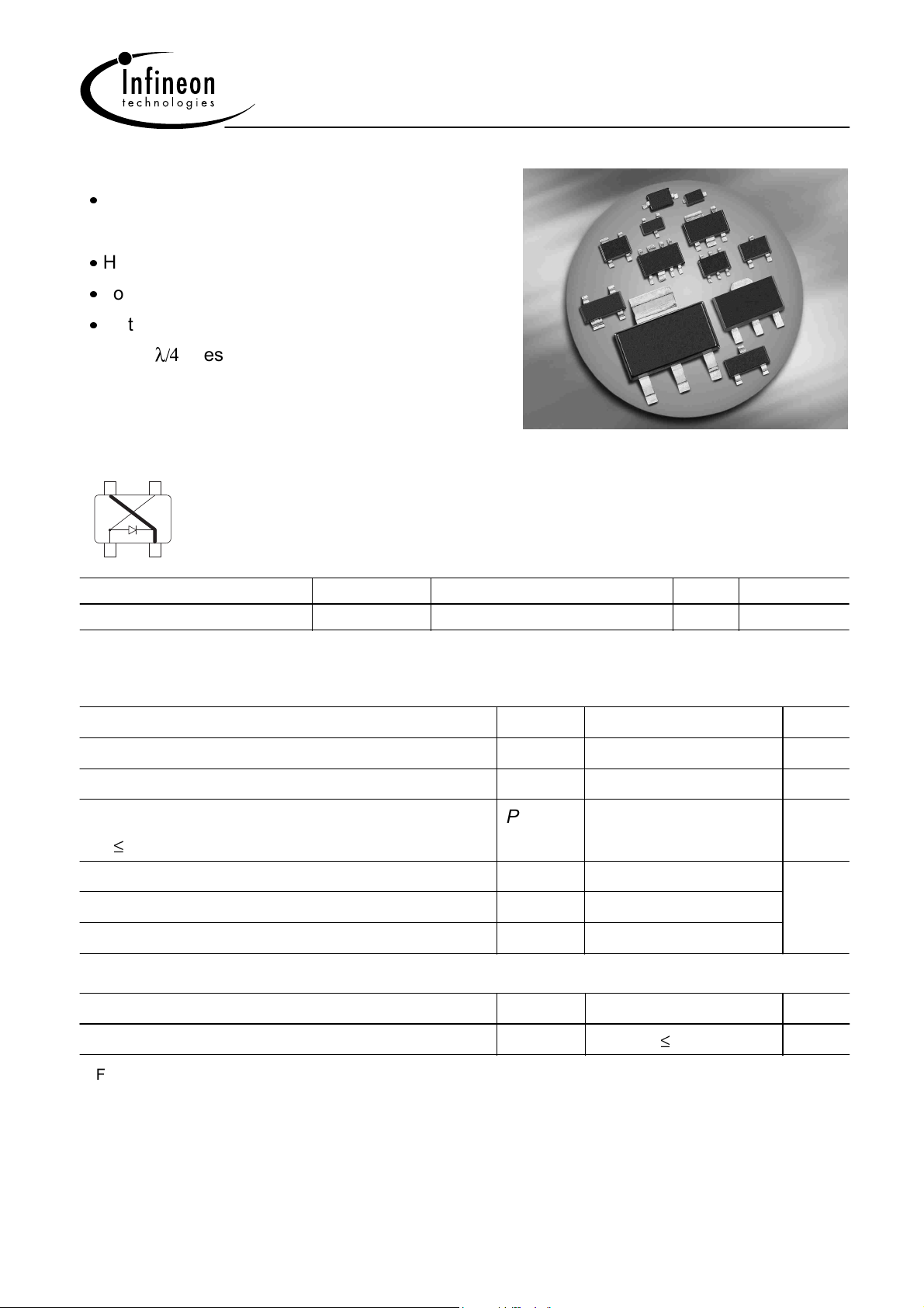
Silicon RF Switching Diode
Designed for use in shunt configuration in
high performance RF switches
High shunt signal isolation
Low shunt insertion loss
Optimized for short - open transformation
BAR81...
using
lines
BAR81W
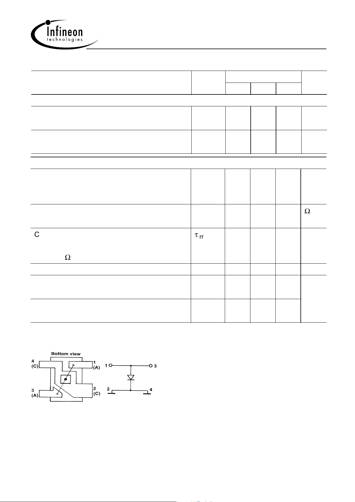
4 3
21
Type Package Configuration L
(nH) Marking
S
BAR81W SOT343 single shunt-diode 0.15* BBs
* series inductance chip to ground
Maximum Ratings at TA = 25°C, unless otherwise specified
Parameter
Diode reverse voltage V
Forward current I
Total power dissipation
T
138°C
s
Symbol Value Unit
30 V
100 mA
100 mW
P
R
F
tot
Junction temperature T
Operating temperature range T
Storage temperature T
Thermal Resistance
Parameter
Junction - soldering point
1
For calculation of R
thJA
1)
please refer to Application Note Thermal Resistance
1
j
op
stg
150 °C
-55 ... 125
-55 ... 150
Symbol Value Unit
R
thJS
120
K/W
Dec-20-2002
Electrical Characteristics at TA = 25°C, unless otherwise specified
BAR81...
Parameter
DC Characteristics
Reverse current
V
= 20 V
R
Forward voltage
I
= 100 mA
F
AC Characteristics
Diode capacitance
= 1 V, f = 1 MHz
V
R
V
= 3 V, f = 1 MHz
R
Forward resistance
= 5 mA, f = 100 MHz
I
F
Charge carrier life time
= 10 mA, IR = 6 mA, measured at IR = 3 mA,
I
F
R
= 100
L
Symbol Values Unit
min. typ. max.
- - 20
nA
- 0.93 1 V
-
-
0.6
0.57
0.9
- 0.7 1
1
pF
- 80 - ns
C
r
I
V
R
F
T
f
rr
I-region width W
Shunt insertion loss1)
= 3 V, f = 1.89 GHz
V
R
Shunt isolation1)
= 10 mA , f = 1.89 GHz
I
F
|S21|
|S21|
Configuration of the shunt-diode
- A perfect ground is essential for optimum isolation
- The anode pins should be used as passage for RF
1
For more information please refer to Application Note 049.
I
2
2
- 3.5 - µm
- 0.7 - dB
- 30 -
2
Dec-20-2002

BAR81...
Diode capacitance CT = (VR)
f = Parameter
1
F
0.8
T
0.7
C
0.6
0.5
1 MHz ... 1.8 GHz
0.4
0.3
0.2
0 2 4 6 8 10 12 14 16
Reverse parallel resistance RP = (VR)
f = Parameter
4
10
KOhm
3
10
p
2
10
R
1
10
0
10
-1
V
20
V
R
10
0 2 4 6 8 10 12 14 16
100 MHz
1 GHz
1.8 GHz
V
20
V
R
Forward resistance rf = (IF)
f = 100MHz
1
10
Ohm
f
r
0
10
-1
10
10
-2
10
-1
10
0
10
Forward current IF = (VF)
= Parameter
T
A
0
10
A
-1
10
-2
10
F
I
-3
10
-40 °C
25 °C
-4
10
-5
10
-6
1
I
mA
F
10
2
10
0 0.2 0.4 0.6 0.8
85 °C
125 °C
V
V
1.2
F
3
Dec-20-2002

BAR81...
Forward current IF = (TS)
BAR81W
120
mA
100
90
80
F
I
70
60
50
40
30
20
10
0
0 15 30 45 60 75 90 105 120
°C
Permissible Puls Load R
thJS
= (tp)
BAR81W
3
10
K/W
2
10
thJS
R
0.5
10
0.2
0.1
0.05
0.02
0.01
0.005
D = 0
-3
10
-2
s
t
0
10
P
1
10
0
10
150
T
S
10
-6
10
-5
10
-4
Permissible Pulse Load
I
Fmax
FDC
/I
Fmax
I
/ I
10
-
10
10
= (tp) BAR81W
FDC
2
1
0
10
-6
10
-5
10
-4
10
D = 0
0.005
0.01
0.02
0.05
0.1
0.2
0.5
-3
10
-2
s
t
0
10
P
4
Dec-20-2002

This datasheet has been download from:
www.datasheetcatalog.com
Datasheets for electronics components.
 Loading...