

Infineon BAR63-02L, BAR63-02V, BAR63-02W, BAR63-03W, BAR63-04 Schematic [ru]
...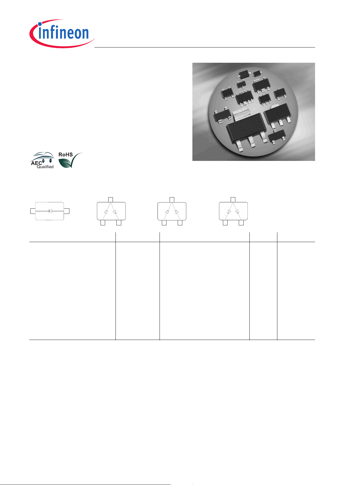
Silicon PIN Diodes
• PIN diode for high speed
switching of RF signals
• Very low forward resistance (low insertion loss)
• Very low capacitance (high isolation)
• For frequencies up to 3GHz
• Pb-free (RoHS compliant) package
• Qualified according AEC Q101
1)
BAR63...
BAR63-02..
BAR63-03W
BAR63-04
BAR63-04W
!
,
,
BAR63-05
BAR63-05W
!
,
,
BAR63-06
BAR63-06W
!
,
,
Type Package Configuration L
BAR63-02L*
BAR63-02V
BAR63-02W
BAR63-03W
BAR63-04
BAR63-04W
BAR63-05
BAR63-05W
BAR63-06
BAR63-06W
TSLP-2-1
SC79
SCD80
SOD323
SOT23
SOT323
SOT23
SOT323
SOT23
SOT323
single, leadless
single
single
single
series
series
common cathode
common cathode
common anode
common anode
(nH) Marking
S
0.4
0.6
0.6
1.8
1.8
1.4
1.8
1.4
1.8
1.4
G
G
GG
white G
G4s
G4s
G5s
G5s
G6s
G6s
1
*BAR63-02L is not qualified according AEC Q101
1
2011-07-18
Maximum Ratings at TA = 25°C, unless otherwise specified
g
BAR63...
Parameter
Symbol Value Unit
Diode reverse voltage V
Forward current I
Total power dissipation
BAR63-02L, T
≤ 118°C
S
BAR63-02V, -02W, BAR63-03W, T
BAR63-04...BAR63-06, T
BAR63-04S, T
≤ 115°C
S
BAR63-04W...BAR63-06W, T
≤ 55°C
S
≤ 105°C
S
≤ 115°C
S
P
Junction temperature T
Operating temperature range T
Storage temperature T
Thermal Resistance
Parameter
Junction - soldering point1)
Symbol Value Unit
R
BAR63-02L
R
F
tot
j
op
st
thJS
50 V
100 mA
250
250
250
250
250
150 °C
-55 ... 125
-55 ... 150
≤ 125
mW
K/W
BAR63-02V, BAR63-02W
BAR63-03W
BAR63-04...BAR63-06
BAR63-04S
BAR63-04W...BAR63-06W
Electrical Characteristics at TA = 25°C, unless otherwise specified
Parameter
Symbol Values Unit
min. typ. max.
DC Characteristics
Breakdown voltage
I
= 5 µA
(BR)
Reverse current
V
= 35 V
R
Forward voltage
I
= 100 mA
F
V
I
V
R
(BR)
F
50 - - V
- - 10
- 0.95 1.2 V
≤ 140
≤ 155
≤ 380
≤ 180
≤ 180
nA
1
For calculation of R
please refer to the Technical Information
thJA
2
2011-07-18

Electrical Characteristics at TA = 25°C, unless otherwise specified
BAR63...
Parameter
AC Characteristics
Diode capacitance
V
= 5 V, f = 1 MHz
R
V
= 0 V, 100 MHz ... 1.8 GHz
R
Reverse parallel resistance
V
= 0 V, f = 100 MHz
R
V
= 0 V, f = 1 GHz
R
V
= 0 V, f = 1.8 GHz
R
Forward resistance
I
= 5 mA, f = 100 MHz
F
I
= 10 mA, f = 100 MHz
F
Charge carrier life time
I
= 10 mA, IR = 6 mA, measured at IR = 3 mA,
F
R
= 100 Ω
L
Symbol Values Unit
min. typ. max.
C
R
r
τ
T
-
-
P
-
-
-
f
-
-
rr
- 75 - ns
0.21
0.3
500
15
5
1.2
1
0.3
pF
-
kΩ
-
-
-
Ω
2
-
I-region width W
Insertion loss1)
I
= 1 mA, f = 1.8 GHz
F
I
= 5 mA, f = 1.8 GHz
F
I
= 10 mA, f = 1.8 GHz
F
Isolation1)
V
= 0 V, f = 0.9 GHz
R
V
= 0 V, f = 1.8 GHz
R
V
= 0 V, f = 2.45 GHz
R
Series inductance L
1
BAR63-02L in series configuration, Z = 50Ω
I
L
I
SO
I
S
- 4.5 - µm
-
-
-
-
-
-
0.15
0.11
0.1
17.9
12.3
10
dB
-
-
-
-
-
-
- - -
3
2011-07-18
BAR63...
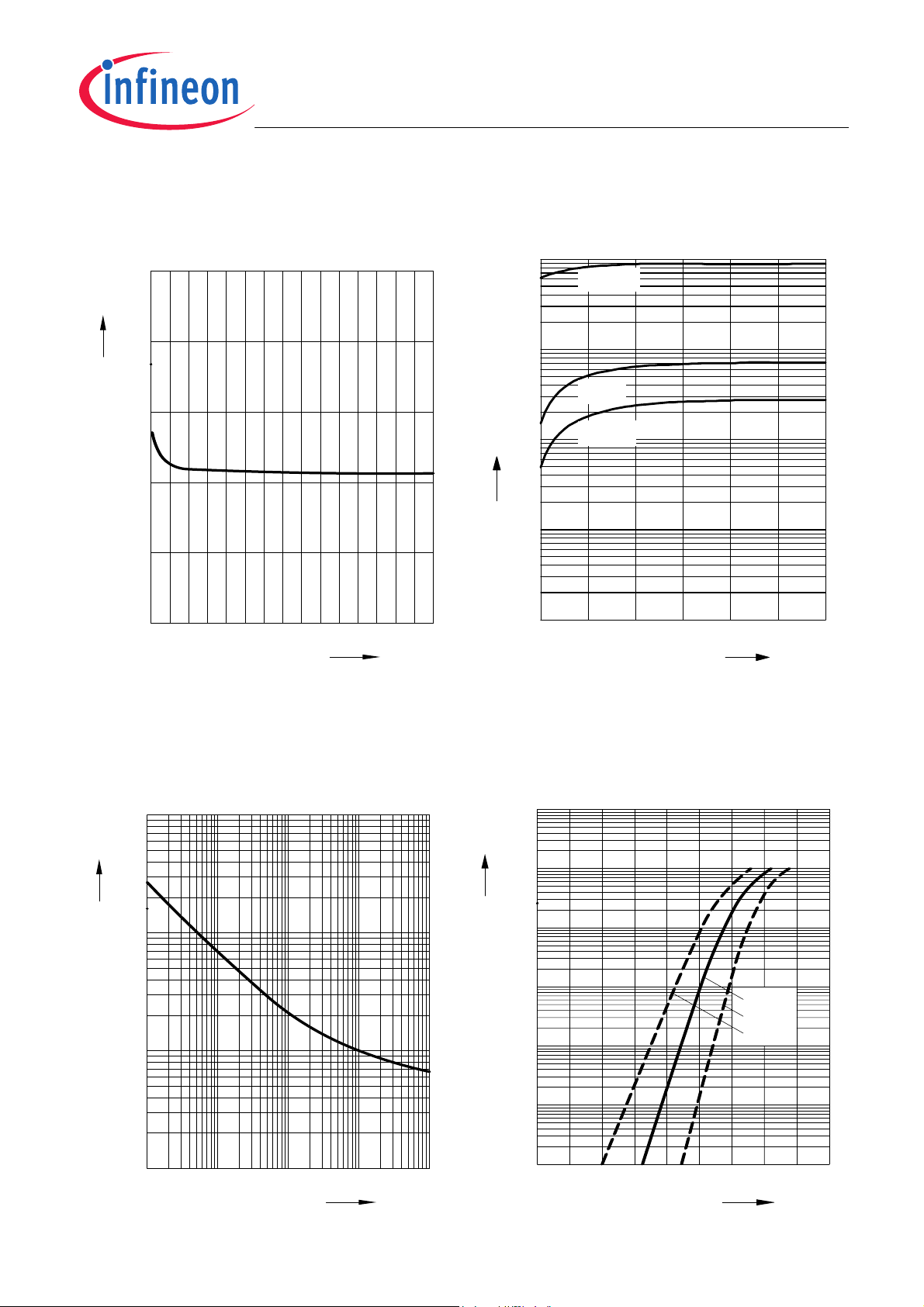
Diode capacitance CT = ƒ (VR)
f = 1MHz - 1.8GHz
0.5
pF
C
T
0.4
0.3
0.2
0.1
0
0V
10 20 30
EHD07139
V
R
Reverse parallel resistance RP = ƒ(VR)
f = Parameter
3
10
KOhm
p
R
10
10
10
10
2
1
0
-1
100 MHz
1 GHz
1.8 GHz
0 5 10 15 20
V
V
R
30
Forward resistance rf = ƒ (IF)
f = 100MHz
2
10
Ω
r
f
1
10
0
10
-1
10
10
-2
10
-1
10
0
10
EHD07138
1
mA
Ι
F
10
Forward current IF = ƒ (VF)
T
= Parameter
A
BAR 63...
3
10
mA
Ι
F
2
10
1
10
0
10
-1
10
-2
10
-3
10
2
0.3
0.5 0.8 1 V 1.2
25 ˚C
40
85˚C˚C
EHD07171
V
F
4
2011-07-18
BAR63...
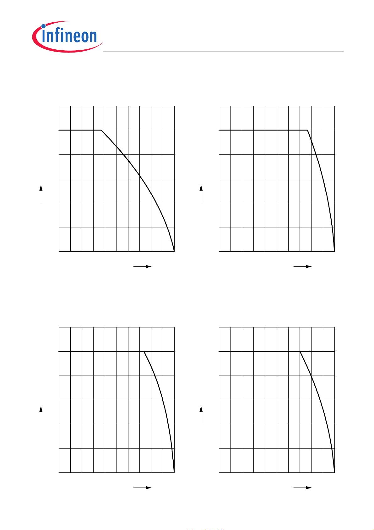
Forward current IF = ƒ (TS)
BAR63-04...BAR63-06
120
mA
80
F
I
60
40
20
0
0 15 30 45 60 75 90 105 120
Forward current IF = ƒ (TS)
BAR63-02V, BAR63-02W
120
mA
80
F
I
60
40
20
°C
150
T
S
0
0 15 30 45 60 75 90 105 120
°C
150
T
S
Forward current IF = ƒ (TS)
BAR63-03W
120
mA
80
F
I
60
40
20
0
0 15 30 45 60 75 90 105 120
Forward current IF = ƒ (TS)
BAR63-04W...BAR63-06W
120
mA
80
F
I
60
40
20
°C
150
T
S
0
0 15 30 45 60 75 90 105 120
°C
150
T
S
5
2011-07-18
BAR63...
Permissible Puls Load R
BAR63-04...BAR63-06
5
K/W
R
thJS
2
10
5
1
10
5
t
D =
T
0
10
10-610-510-410-310
P
thJS
= ƒ (tp)
D=
0.5
0.2
0.1
0.05
0.05
0.01
0.005
0
t
P
T
-2
EHB07146
s10
t
P
0
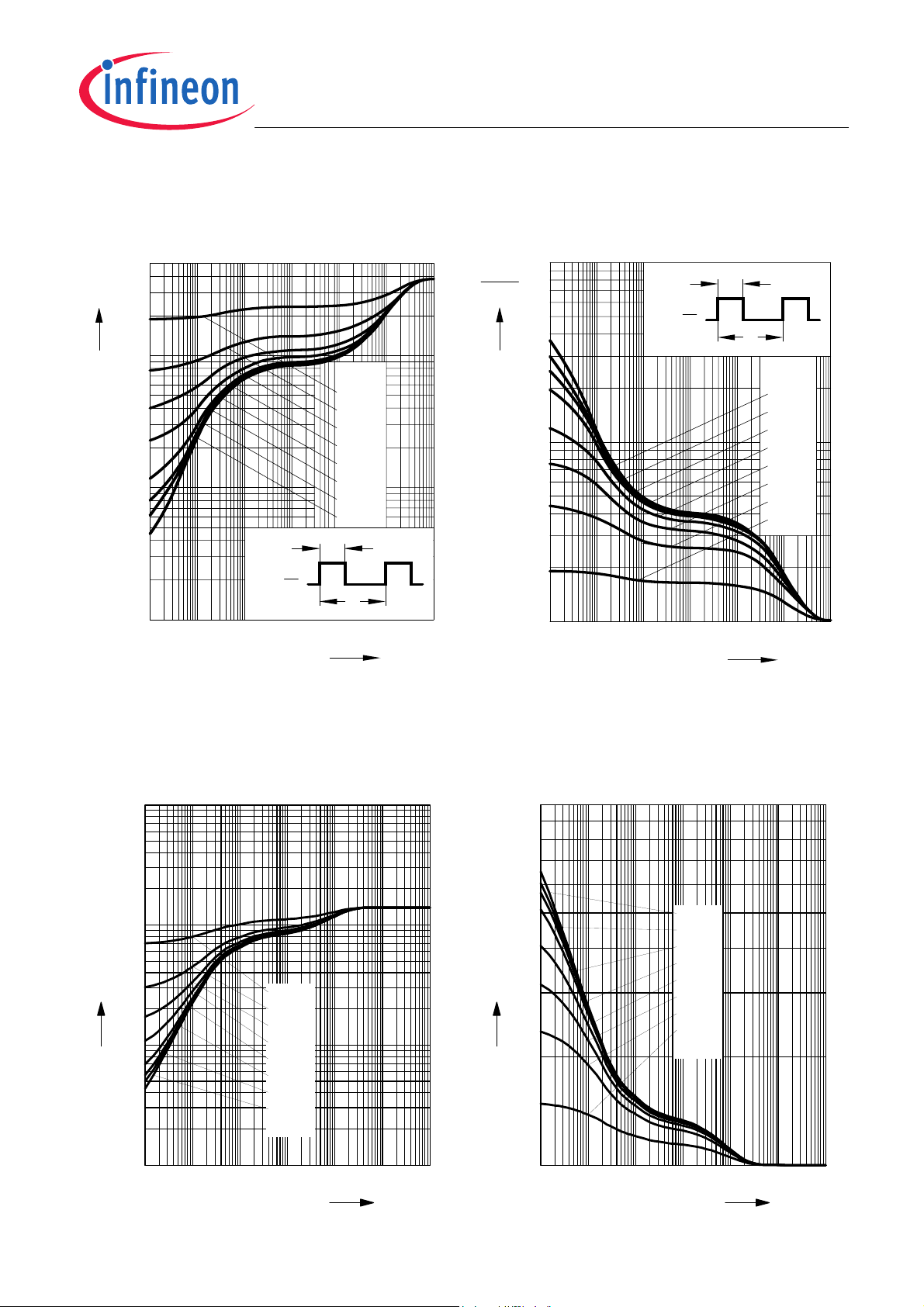
Permissible Pulse Load
I
Fmax
/ I
FDC
= ƒ (tp)
BAR63-04...BAR63-06
2
10
Ι
F
max
Ι
DC
F
5
1
10
5
0
10
10-610-510-410-310
D =
EHB07147
t
P
t
P
T
T
D=
0
0.005
0.01
0.02
0.05
0.1
0.2
0.5
-2
s10
t
P
0
Permissible Puls Load R
BAR63-02V, BAR63-02W
3
10
K/W
2
10
thJS
R
0.5
0.2
10
-4
0.1
0.05
0.02
0.01
0.005
D = 0
10
10
10
1
0
10
-6
10
-5
thJS
-3
= ƒ (tp)
-2
10
Permissible Pulse Load
I
Fmax
/ I
FDC
= ƒ (tp)
BAR63-02V, BAR63-02W
1
10
/ IFDC
Fmax
I
-
0
s
t
0
10
p
10
10
-6
10
-5
10
D = 0
0.005
0.01
0.02
0.05
0.1
0.2
0.5
-4
10
-3
10
-2
s
t
0
10
p
6
2011-07-18
 Loading...